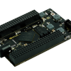
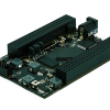
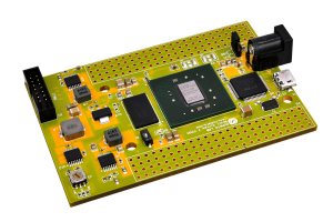
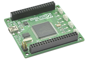
Neso – A7 FPGA Development Board
SKU: FPGA009
Request For QuoteWanna Customize? Drop Us A Line!
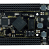
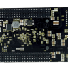
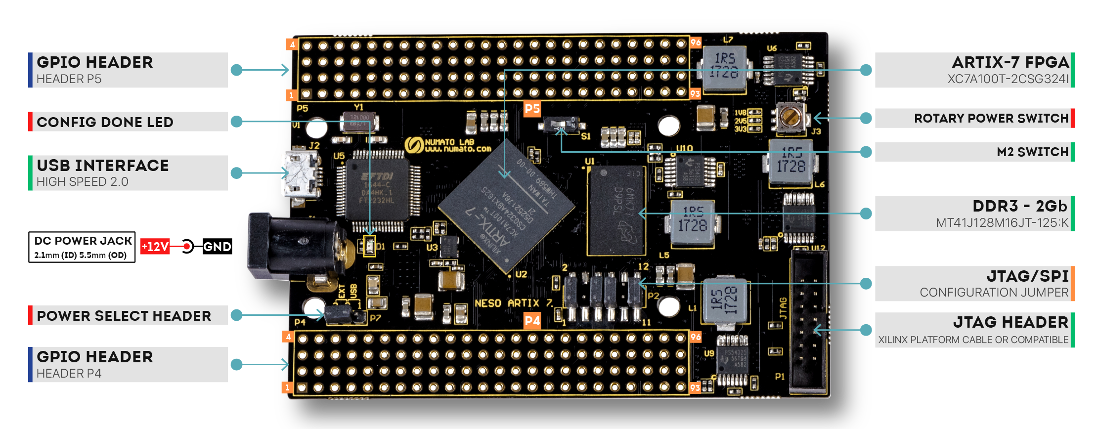
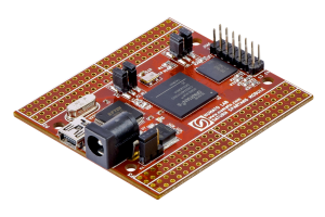
Neso is an easy to use FPGA Development board featuring Artix 7 FPGA. It is specially designed for the development and integration of FPGA based accelerated features to other designs. This development board features Xilinx XC7A100T FPGA with FTDI’s FT2232H Dual-Channel USB device. Xilinx Artix 7 offers the best system performance per watt in class and is a great choice for cost-sensitive applications. The high-speed USB 2.0 interface provides fast and easy configuration download to the onboard SPI flash. No programmer or special downloader cable is needed to download the bitstream to the board.
Features
- FPGA: XC7A100T in CSG324 package (XC7A100T-2CSG324C)
- DDR3: 2Gb DDR3(MT41J128M16JT-125:K)
- Flash memory: 128 Mb SPI flash memory (N25Q128A13ESE40E / IS25LP128F – JBLE)
- 100MHz CMOS oscillator
- High-Speed USB 2.0 interface for Onboard flash programming.
- Revision V1: FT2232H Channel A is dedicated to SPI Flash /JTAG Programming. Channel B can be used for custom applications.
- Revision V2: FT2232H Channel B is dedicated to SPI Flash /JTAG Programming. Channel A can be used for custom applications.
- Onboard voltage regulators for single power rail operation
- FPGA configuration via JTAG and USB
- Compact form factor FPGA Module
- Maximum IOs for user-defined purposes
- FPGA – 140 IOs
- FT2232H – 8 IOs
Knowledge Base
Knowledge Base
Specifications
| Attribute | Value |
|---|---|
| Weight | 0.12 lbs |
| Dimensions | 5 × 3 × 1 in |
| Product Dimensions | 3.29 x 2.26 x 0.62 in |
| FPGA | |
| Memory | |
| Primary Clock Frequency | |
| Number Of GPIOs (Max) | |
| Configuration Options | |
| Host Interface | |
| Package Contents | |
| HTS | 8542.39.0001 |
| ECCN | 3A991.d |
Sample Code
Sample Code
| Name | Language/Technology | IDE | Hardware Modules Required |
|---|---|---|---|
| 16x2 LCD Display | Verilog | Xilinx Vivado | Saturn IO Breakout Module Alphanumeric LCD Display Expansion Module |
| 8Bit VGA | Verilog | Xilinx Vivado | Saturn IO Breakout Module VGA Display Expansion Module |
| CS4344 Stereo Audio | Verilog | Xilinx Vivado | Saturn IO Breakout Module CS4344 Audio Expansion Module |
| HDMI Transmitter | VHDL | Xilinx Vivado | Saturn IO Breakout Module HDMI Transmitter Expansion Module |

