Mandelbrot Fractal Output, Simple HDMI + VGA Framebuffer Design using Neso
Introduction
Framebuffer refers to a memory (or an area within a memory) which is dedicated for storing the pixel data. A frame is a collection of pixels which make up the complete image to be displayed on a screen and buffer refers to memory which stores these pixels, hence the name “Framebuffer“. Dedicated hardware is typically used to copy the pixels from the memory and display them on screen, aided by a processor if needed. Framebuffers are very commonly used because generating pixels in real-time and displaying them on screen is a very difficult task. So, the generated pixels are first stored in the framebuffer, and then, the content of the framebuffer is copied to display. In Fact, it is extremely likely that on the device on which you are reading this article, the pixel data on the screen is coming from a framebuffer itself which was written to earlier with pixel data by a graphics engine. This article will show a simple framebuffer design which can output pixel data to HDMI and well as VGA simultaneously using Neso Artix 7 FPGA Module.
Prerequisites
Following hardware and software are required to follow this article:
- Neso Artix 7 FPGA Module (variant with female headers on top)
- IO Breakout Module for Saturn
- HDMI Transmitter Expansion Module
- VGA Display Expansion Module
- Xilinx Platform Cable USB II JTAG Hardware
- Xilinx Vivado 2017.3 or higher
- 9V DC Power Supply for Neso
Familiarity with Vivado and its IP Integrator flow, VGA, HDMI, AXI4 and AXI4-Stream protocols is also necessary to follow the article.
Download and install Vivado Board Support Package files for Neso from here. Follow the README.md file on how to install Vivado Board Support Package files for Numato Lab boards. You may skip this step if you already installed the Vivado Board Support Package files for Numato Lab boards in the past while following other articles.
Architecture
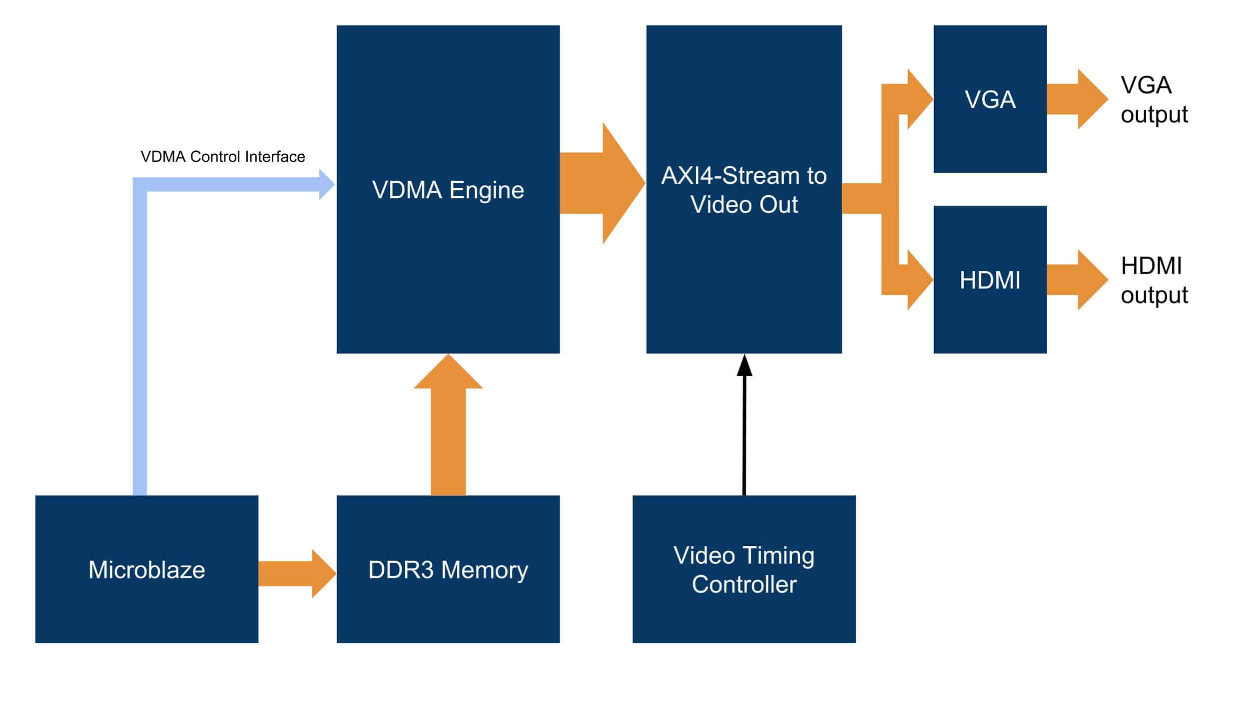
Architecture of Simple VGA & HDMI Framebuffer Design
The architecture of the Simple VGA & HDMI Framebuffer Design is shown above. It has the following blocks:
- VGA and HDMI blocks: These two blocks fetch pixel data from the “AXI4-Stream to Video Out” block and display them over VGA and HDMI respectively.
- Video Timing Controller block: This block generates the video timing signals which is used by “AXI4-Stream to Video Out” block to synchronize the frames and scanlines. Typical signals are
hsync,vsync,active,blanketc. The “AXI4-Stream to Video Out” block also forwards the timing information to VGA and HDMI blocks. Timing is decided by the resolution and frame-rate (screen refresh frequency). This article uses 800×600@60Hz resolution. - AXI4-Stream to Video Out block: This block converts the AXI-Stream data coming from the VDMA Engine to video. For conversion, this block needs to know the pixel format of the incoming data. For this article, the pixel format RBG888 is used. This means each pixel is of 3 bytes, one byte (8-bits) for each of the three colors. So, a total of 24 bits per pixel.
- VDMA Engine: VDMA is a short form for Video Direct Memory Access. This is the primary data-mover block. It fetches pixel data from the start of framebuffer region inside DDR3 memory and streams it out via AXI4-Stream protocol to “AXI4-Stream to Video Out” block. For this, VDMA Engine needs to know the start address (or base address) of the framebuffer in the DDR3. It also needs to know the screen resolution and number of framebuffers (this article uses just one), pixel data format (RGB888 in case of this article), etc. All this information is provided to VDMA Engine via VDMA Control Interface which actually is a simple AXI-Lite interface with a number of registers for each configuration parameter. This control interface is also used to start or stop the running of the VDMA engine.
- DDR3 Memory: This block is just the DDR3 memory which stores the framebuffer.
- Microblaze: Microblaze is a 32-bit soft-processor developed by Xilinx. In this article, Microblaze is used for configuring and starting the VDMA engine via the VDMA control interface. It is also used to write to the framebuffer in DDR3 memory with different patterns. So, any data written to the framebuffer will show up on VGA and HDMI outputs. The sample code written for this article cycles through various colors which get displayed on VGA as well as HDMI. After cycling through colors, the sample code then generates a Mandelbrot fractal pattern on the screen.
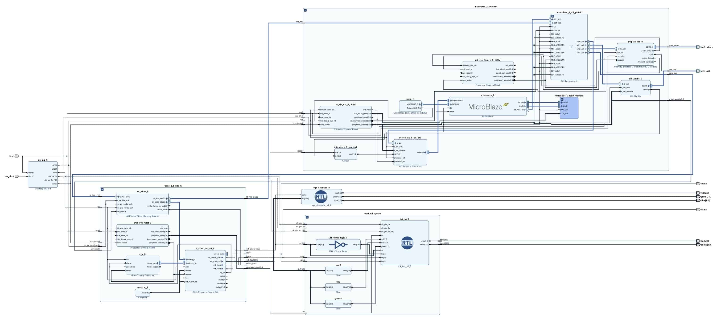
Vivado Block Design
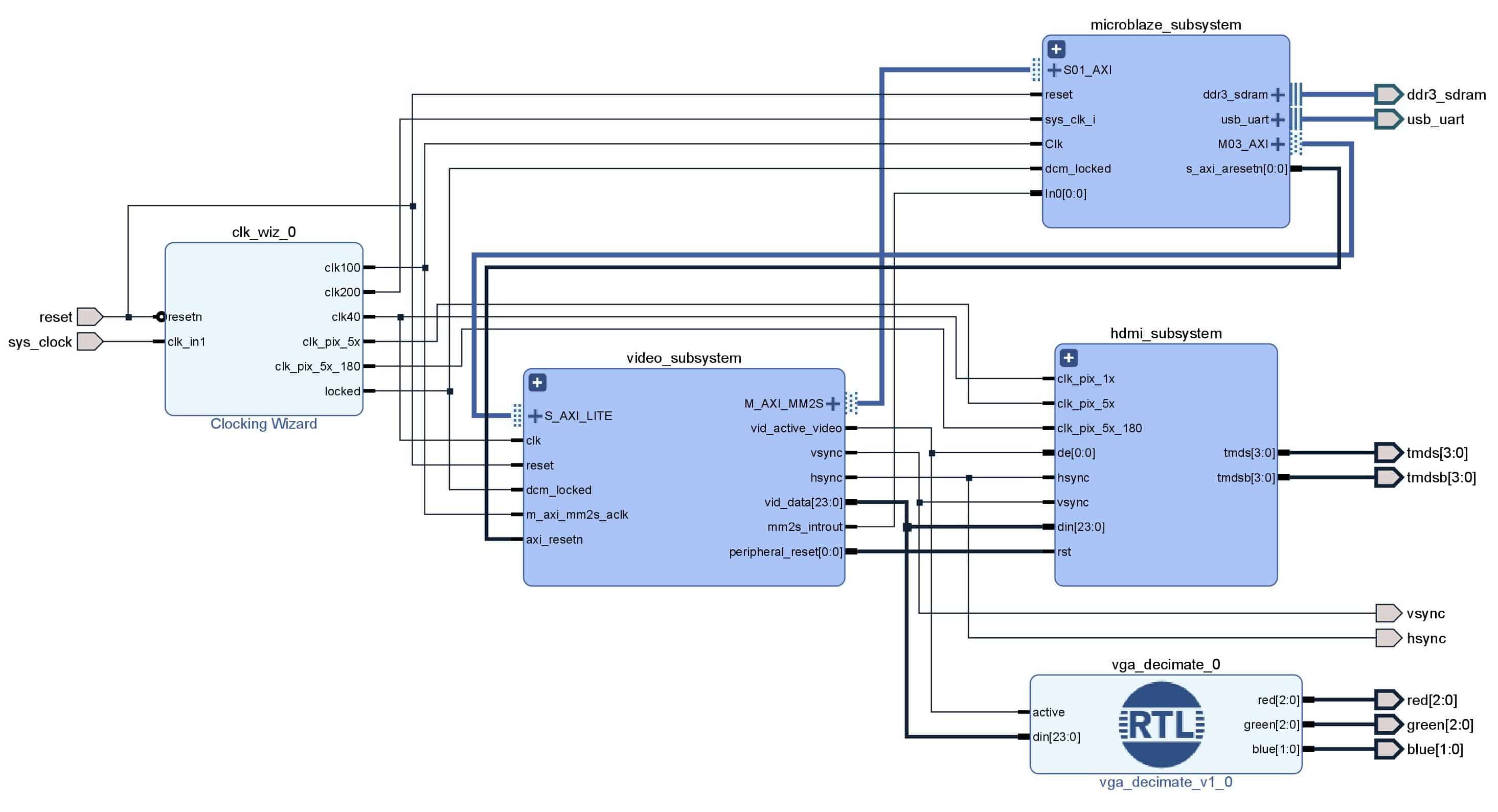
Vivado Condensed Block Design for Simple VGA & HDMI Framebuffer
The condensed block diagram of the Simple VGA and HDMI Framebuffer design hides a lot of complexity into individual subsystems. Readers might notice that the Vivado Block Design shown above doesn’t actually match the architecture diagram discussed before. That is because the architecture is a higher-level diagram and doesn’t go into intricacies such as clock, reset, AXI-interconnects, etc whereas the Vivado Block Diagram is an exact drawing of the real-world, working design running on hardware.
As shown in the above image, there are three subsystems:
- Microblaze Subsystem
- Video Subsystem
- HDMI Subsystem
These subsystems are elaborated later in their own sections.
Apart from these three subsystems, there is one “Clocking Wizard” block and a “vga_decimate” block.
The “Clocking Wizard” block is the clock generator for all the clocks being used in the design. It takes 100 MHz system clock from the oscillator on-board Neso as input and derives other clocks from it. This project uses a total of five clocks:
- 100 MHz: Microblaze and all AXI4 Memory Mapped interface run on this clock.
- 200 MHz: The Xilinx MIG 7 IP core for DDR3 uses this 200MHz for the Memory Controller as well as Reference Frequency.
- 40 MHz: This is the primary pixel clock. It is dependent on resolution. Since this article uses 800×600@60Hz, this pixel clock frequency is 40 MHz
- 5x Pixel Clock = 200 MHz: This clock is 5x of the pixel clock. For 800×600, its frequency comes out at 200MHz. This clock along with its inverted version (180 degrees out of phase) is used by HDMI subsystem to serialize pixel data at 10x of pixel clock frequency.
- Inverted 5x Pixel Clock: Already mentioned above. It is used by HDMI subsystem to serialize pixel data at 10x of pixel clock frequency.
The “vga_decimate” block is a simple RTL Verilog file used to down-convert the 24-bits per pixel to 8-bits per pixel since the VGA Display Expansion Module supports only 8-bits per pixel. Vivado allows adding users’ RTL files to block designs and this project uses RTL block for the HDMI subsystem also.
Microblaze Subsystem
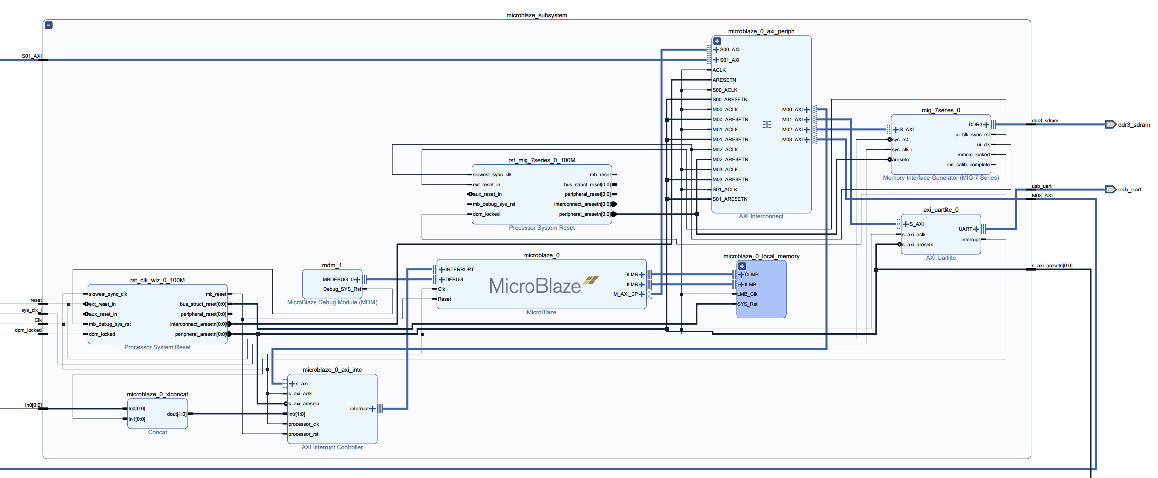
Microblaze Subsystem
The Microblaze subsystem has Microblaze soft-processor, Microblaze Debug Module (MDM), Local Memory (BRAM), Processor System Reset (Reset Generators), AXI Interrupt Controller, Concat, AXI Interconnect, AXI Uartlite, and MIG 7 IP core blocks. Microblaze is the processor overseeing the entire design and is used for configuring and starting the VDMA Engine. It is also used to communicate with the host system via UART using AXI Uartlite IP Core and prints out useful debug messages over UART. The MIG 7 IP core is the DDR3 controller necessary for interfacing with DDR3 memory on Neso. AXI interconnect connects all the AXI masters and AXI slaves together. AXI masters have the capability to initiate memory transactions, whereas AXI slaves can only respond to the transactions initiated by the AXI masters.
There are two AXI masters in the design: Microblaze and VDMA. It makes sense since both the Microblaze and VDMA engine require the capability to initiate memory transactions. Microblaze has to control all peripherals such as UART, Interrupt Controller, etc and also has to write different patterns and data to the framebuffer and VDMA has to initiate read transactions to read pixel data from the framebuffer.
There are four AXI slaves in the design: DDR3 (MIG 7 IP core), UART (AXI Uartlite IP Core), Interrupt Controller (AXI Interrupt Controller) and VDMA (VDMA Control Interface).
Most of the blocks in Microblaze subsystem (MDM, Local Memory Block, etc) are automatically created and connected by Vivado as part of “Block Automation” and “Connection Automation” process of Vivado IP Integrator flow. This is why familiarity with Vivado IP Integrator workflow was a prerequisite for this article. Readers need not to connect most of the blocks manually, Vivado should be able to handle it automatically.
Video Subsystem
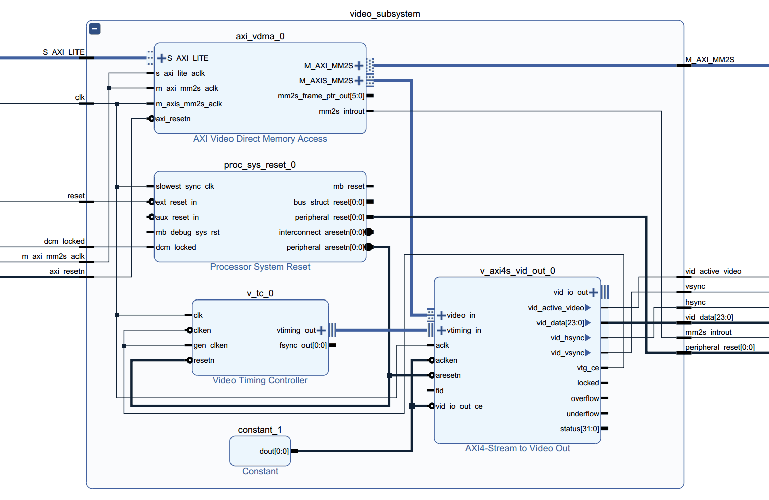
Video Subsystem
The Video Subsystem is comparatively simpler in terms of connections and number of blocks to Microblaze. It comprises “AXI Video Direct Memory Access” IP block, “Video Timing Controller” IP block, “AXI4-Stream to Video Out” IP block, “Processor System Reset” IP block and “Constant” IP block. Functions of VDMA, Video Timing Controller and AXI4-Stream to Video Out blocks have already been explained in the architecture section. Apart from these three, there is one reset generator for the 40 MHz pixel clock. Readers might notice that while the AXI4 Memory Mapped interfaces ran at 100 MHz, the AXI4-Stream interface is running at 40 MHz (subsystem port “clk” connected to “m_axis_mm2s_aclk”. “axis” stands for AXI-Stream). There is one more block named “Constant”. This block is the simplest one. It just drives the constant value of “1” thus enabling “aclken” and “vid_io_out_ce”.
HDMI Subsystem
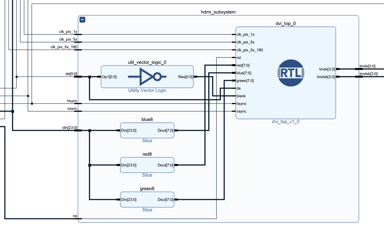
HDMI Subsystem
The usage of the word “HDMI” is little misleading here since the actual output is DVI. But HDMI is a superset of DVI (or to paraphrase, DVI is a subset of HDMI), and so all HDMI receivers should be able to receive DVI signals perfectly. The HDMI Subsystem comprises Utility Vector Logic block, Slice blocks and an RTL block “dvi_top”. The Utility Vector Logic here just works as a NOT gate to invert “de” (data enable) signal to connect to “blank” input of RTL block. The “Slice” blocks break the 24-bit pixel data into individual 8-bit red, green and blue components. The “dvi_top” RTL block converts display data into DVI (HDMI Compatible) format.
Complete Vivado Block Design
Complete Elaborated Vivado Block Diagram for Simple HDMI & VGA Framebuffer Design (click for better resolution)
If the block diagram is not clearly visible, readers can refer to the block diagram PDF: Neso HDMI VGA Framebuffer Block Diagram
Firmware
VDMA Configuration and Initialization
For the framebuffer design to work, the VDMA engine should be configured correctly and finally, the engine should be started. Using Xilinx ‘vdma’ standalone drivers, the VDMA engine can be configured, initialized and started by following these steps:
- Lookup VDMA IP block configuration using
XAxiVdma_LookupConfig()function. - Initialize the DMA engine with configuration data retrieved from the previous step using
XAxiVdma_CfgInitialize()function - Configure DMA (Horizontal resolution, Vertical resolution, Stride, Enable Circular Buffer, etc) using
XAxiVdma_DmaConfig()function - Set VDMA starting address using
XAxiVdma_DmaSetBufferAddr()function - Finally, start the VDMA engine using
XAxiVdma_DmaStart()function
Refer to the Xilinx AXI VDMA Standalone Driver Documentation here for official documentation of the above functions.
The following self-explanatory code illustrates the complete VDMA initialization, configuration, and starting procedure:
int run_frame_buffer(int device_id, int hsize, int vsize) {
	int status;
	XAxiVdma_Config *Config;

	Config = XAxiVdma_LookupConfig(device_id);
	if (!Config) {
		xil_printf("No video DMA found for ID %d\r\n", device_id );
		return XST_FAILURE;
	}

	/* Initialize DMA engine */
	status = XAxiVdma_CfgInitialize(&InstancePtr, Config, Config->BaseAddress);
	if (status != XST_SUCCESS) {
		xil_printf("Configuration Initialization failed, status: 0x%X\r\n", status);
		return status;
	}

	u32 stride = hsize * (Config->Mm2SStreamWidth>>3);

	/* ************************************************** */
	/*           Setup the read channel                   */
	/*                                                    */
	/* ************************************************** */
	ReadCfg.VertSizeInput       = vsize;
	ReadCfg.HoriSizeInput       = stride;
	ReadCfg.Stride              = stride;
	ReadCfg.FrameDelay          = 0;      /* This example does not test frame delay */
	ReadCfg.EnableCircularBuf   = 1;      /* Only 1 buffer, continuous loop */
	ReadCfg.EnableSync          = 0;      /* Gen-Lock */
	ReadCfg.PointNum            = 0;
	ReadCfg.EnableFrameCounter  = 0;      /* Endless transfers */
	ReadCfg.FixedFrameStoreAddr = 0;      /* We are not doing parking */

	status = XAxiVdma_DmaConfig(&InstancePtr, XAXIVDMA_READ, &ReadCfg);
	if (status != XST_SUCCESS) {
		xil_printf("Read channel config failed, status: 0x%X\r\n", status);
		return status;
	}

	// Initially populate framebuffer with complete white
	fill(0xff, 0xff, 0xff);

	/* Set the buffer addresses for transfer in the DMA engine. This is address first pixel of the framebuffer */
	status = XAxiVdma_DmaSetBufferAddr(&InstancePtr, XAXIVDMA_READ, (UINTPTR *) &srcBuffer);
	if (status != XST_SUCCESS) {
		xil_printf("Read channel set buffer address failed, status: 0x%X\r\n", status);
		return status;
	}
	/************* Read channel setup done ************** */


	/* ************************************************** */
	/*  Start the DMA engine (read channel) to transfer   */
	/*                                                    */
	/* ************************************************** */

	/* Start the Read channel of DMA Engine */
	status = XAxiVdma_DmaStart(&InstancePtr, XAXIVDMA_READ);
	if (status != XST_SUCCESS) {
		xil_printf("Failed to start DMA engine (read channel), status: 0x%X\r\n", status);
		return status;
	}
	/* ************ DMA engine start done *************** */

	return XST_SUCCESS;
}
Running the design on your hardware
Download the project package from here and extract it to a convenient location. Open the “Neso-Framebuffer.xpr” project file in Xilinx Vivado. If your Vivado version is newer than the project’s version, you might need to upgrade the project along with the IP blocks used in the project to the latest version.
Generate the bitstream and export hardware with bitstream included. Launch Xilinx SDK with the exported hardware. Prebuilt bitstream files (both .bit and raw .bin file) are available in the “Bitstream” folder in case you want to try out the design on hardware first.
Hardware Setup
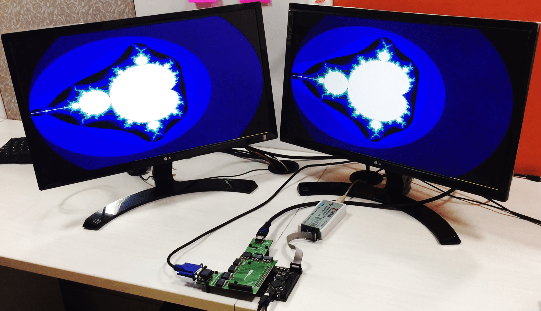
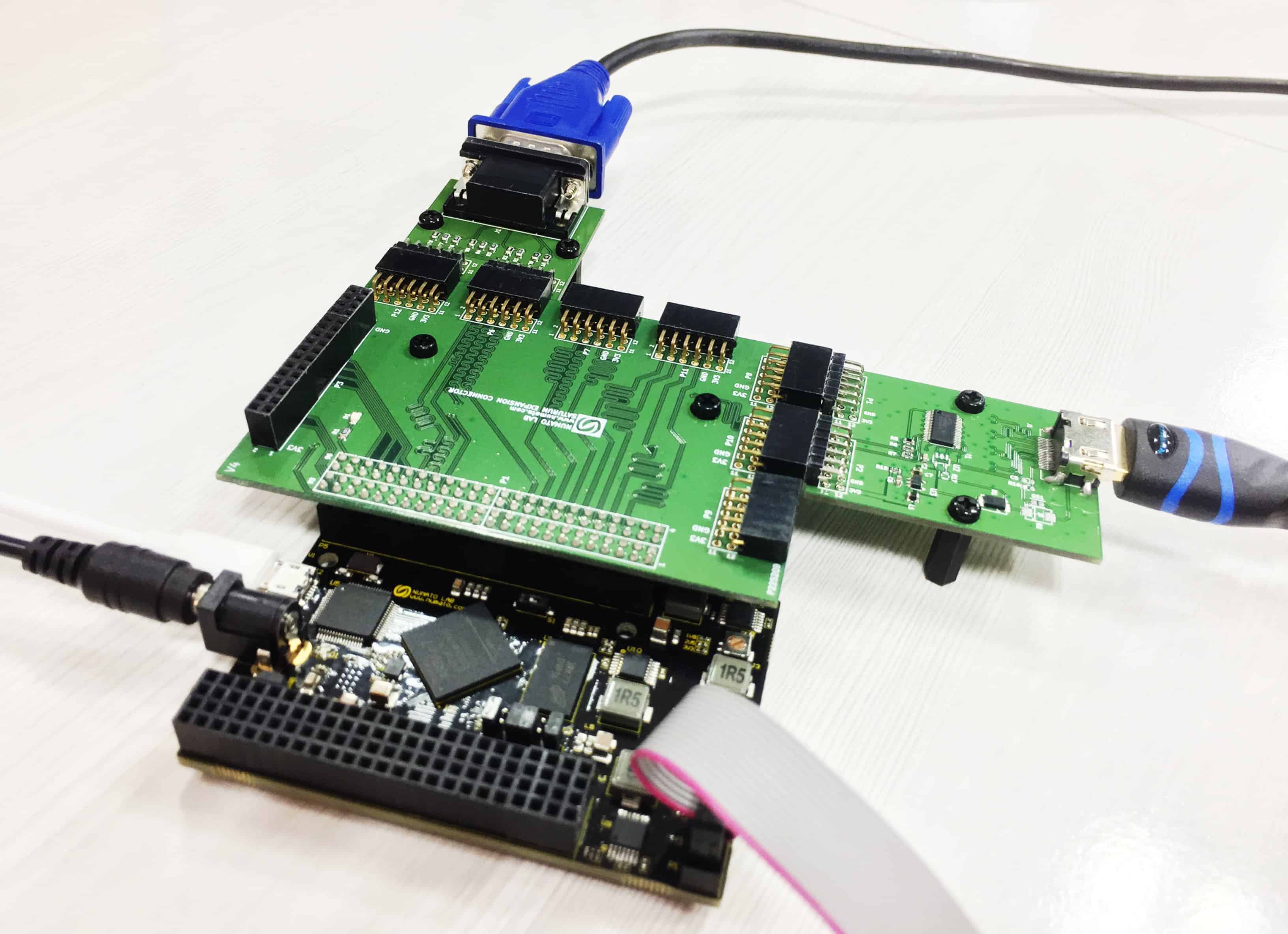
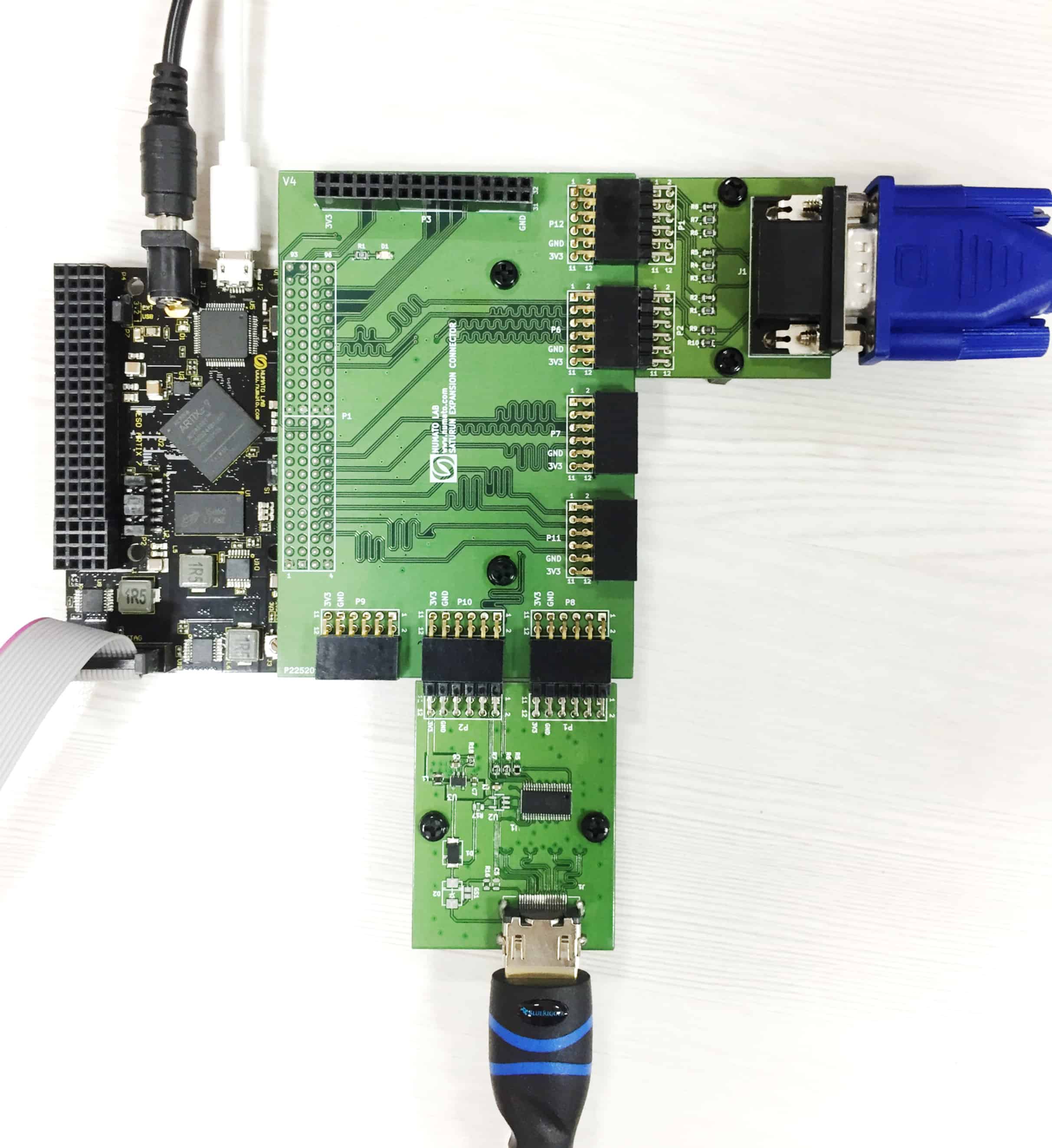
Make sure Neso is powered down and no cables are connected to it. Insert the IO Breakout Module for Saturn into header P5 of Neso Artix 7 FPGA Module. Insert the VGA Display Expansion Module to ports P12 & P6 on the IO Breakout Module. Insert HDMI Transmitter Expansion Module to ports P8 & P10 on the IO Breakout Module. Change the Power-Select jumper on Neso to “EXT” for using external DC Power Supply. Connect USB Micro-B cable to Neso. Then connect Xilinx Platform Cable USB II to the JTAG header on Neso. Also, connect the VGA and HDMI cables to the respective expansion modules and their other ends to monitors. Finally, connect the external DC power supply to power-on the Neso. The hardware connection setup is shown below.
 |
 |
Once the hardware is set up, program Neso with either the prebuilt bitstream available in the “bitstreams” folder or the bitstream generated by you. When using the prebuilt bitstream, the framebuffer demo application will start running automatically and you need not to do anything else. But if you are programming the generated bitstream, either make sure to merge the .ELF firmware into a bitstream or just load the .ELF file to Neso via GDB or System Debugger via Xilinx SDK.
Output
As soon as the FPGA on Neso is programmed with the bitstream and the Microblaze running on it starts the Video-DMA engine, both the monitors connected to VGA and HDMI cables will start displaying exact same pattern, in sync, at 800×600@60Hz resolution. The demo program will cycle through various colors on the screen and then draw a Mandelbrot Pattern on the screen. Once done with Mandelbrot pattern, the firmware again will go back to cycling through various colors and, after that, will start drawing Mandelbrot pattern. This will go on continuously.
Debug Output over UART
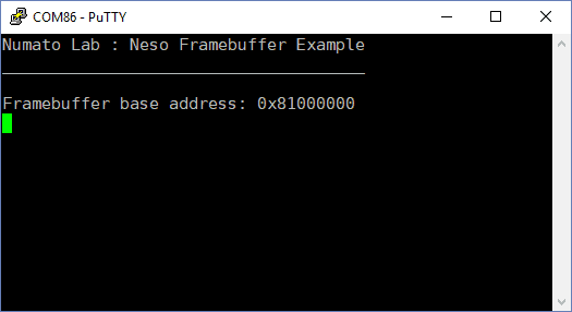
The design logs debug messages over UART which can be viewed using any serial terminal such as PuTTY etc. The baud rate for UART is 115200. Make sure that the Channel B (or Port B) of FT2232H on Neso is configured for RS232/UART. If you followed the Vivado IP Integrator article for Neso, then your Neso is already set up correctly for UART. If the Microblaze encounters any error during initialization, configuration or starting of VDMA engine, it will print the error messages over UART. There are no errors in the above image, so the design is working normally. The UART interface in the design is also used for one secret purpose (hint: head over to the end of the article).
If everything goes well, you should see output similar to as in this video:
If you got the output, congratulations! You have set up your own framebuffer system. Comment below to let others know of your achievement and try to further improve the design. There are lots of possible improvements such as using triple-buffer instead of just a single buffer.
If you didn’t, then worry not, keep trying until you manage to get it working. It is quite difficult to get projects of this level of complexity working at first attempt!
Credits
Huge thanks to Mike Field ‘Hamster’ at http://hamsterworks.co.nz/mediawiki/index.php/FPGA_Projects for the Mandelbrot C code as well as RTL code for the HDMI/DVI transmitter.
Easter Egg
The project has a very visible and possibly exciting easter egg. Try to find it out and comment below if you managed to unlock and use it.