Introduction:
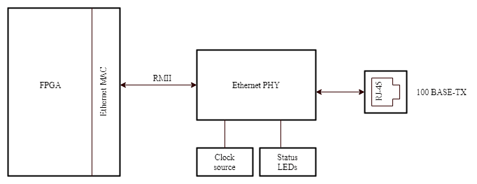
Ethernet is a Link Layer Protocol in the TCP/IP protocol stack between the physical and data link layer. It is the most widely used protocol for Local Area Networks (LANs). Every device on Ethernet is assigned a unique MAC address for communication. The Reduced Media-Independent Interface (RMII) is used to interface Ethernet IP core on FPGA with the Ethernet PHY chip. The Media Access Layer converts the packets into stream of data to be sent while the Physical Layer converts the stream of data into electrical signals. RMII provides a media-independent interface so that there is compatibility between MAC and PHY irrespective of the hardware used. In this tutorial, the Numato Lab 100BASE-T Ethernet Expansion Module is used along with Neso Artix 7 FPGA Module to demonstrate a TCP/IP echo server application. The echo server application runs on light-weight IP (lwIP) TCP/IP stack.
Prerequisites:
- Hardware:
- Neso Artix 7 FPGA Module
- 100Base-T Ethernet Expansion Module
- Ethernet Cable
- Xilinx Platform Cable USB II
- Software:
- Vivado 2022.1 or later
- Telnet terminal (PuTTY etc)
Let’s get Started
Step 1:
Download and install Vivado Board Support Package files for Neso from here. Follow the README.md file on how to install Vivado Board Support Package files for Numato Lab boards.
Step 2:
Open Vivado and select ‘Create Project’
Step 3:
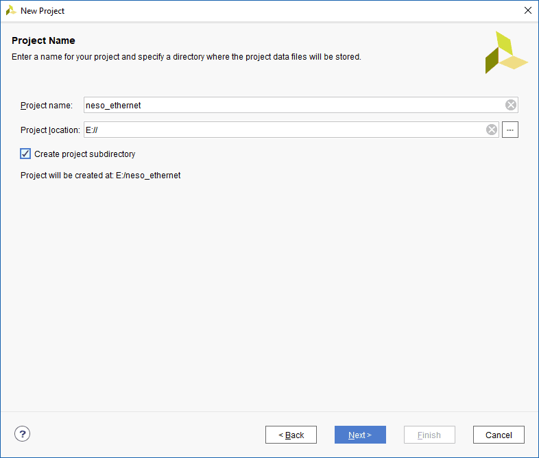
Click ‘Next’. In Project Name tab, give appropriate project name and select the directory where you want to save the project.
Step 4:
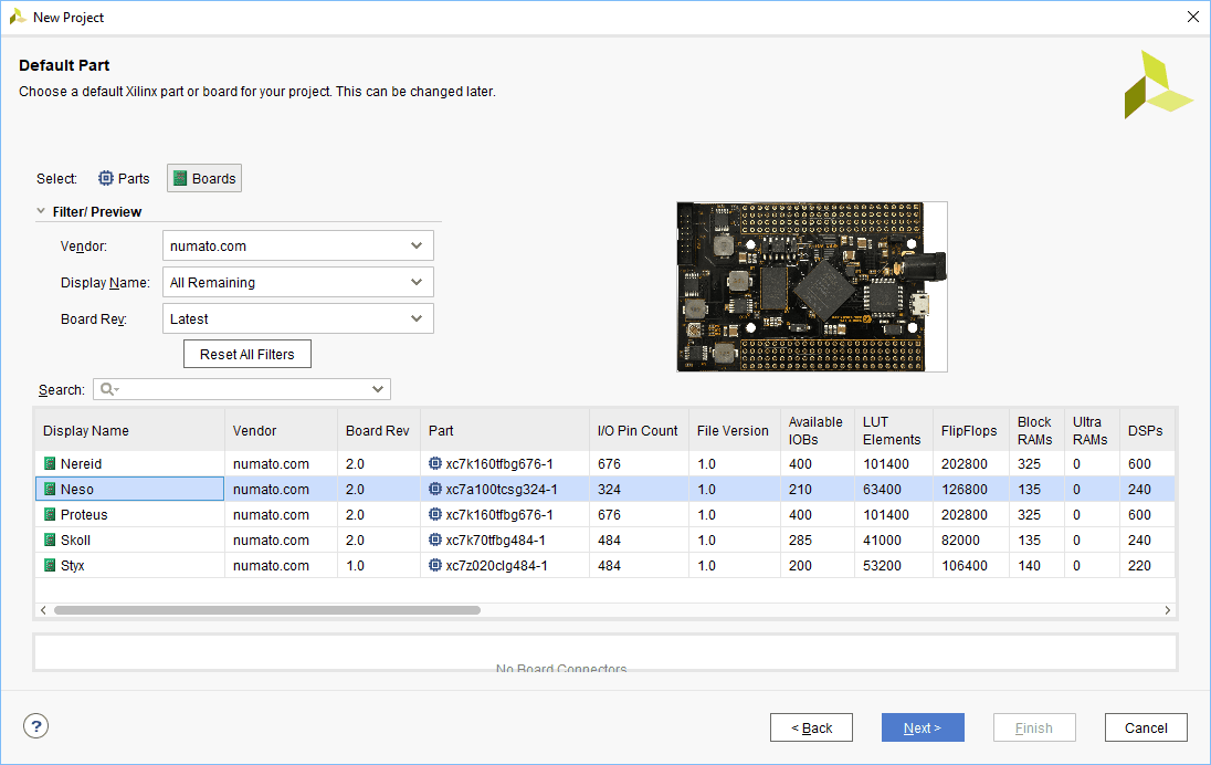
Click Next without making any changes till you see the ‘Default Part’ tab and select ‘Neso’ from ‘Boards’ option. If Neso is not listed, make sure board support files are installed correctly.
Step 5:
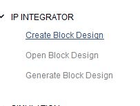
Click ‘Create Block Design’ from IP Integrator and create a block diagram.
Step 6:
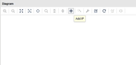
Click ‘Add IP’ in the “Diagram” window
Step 7:
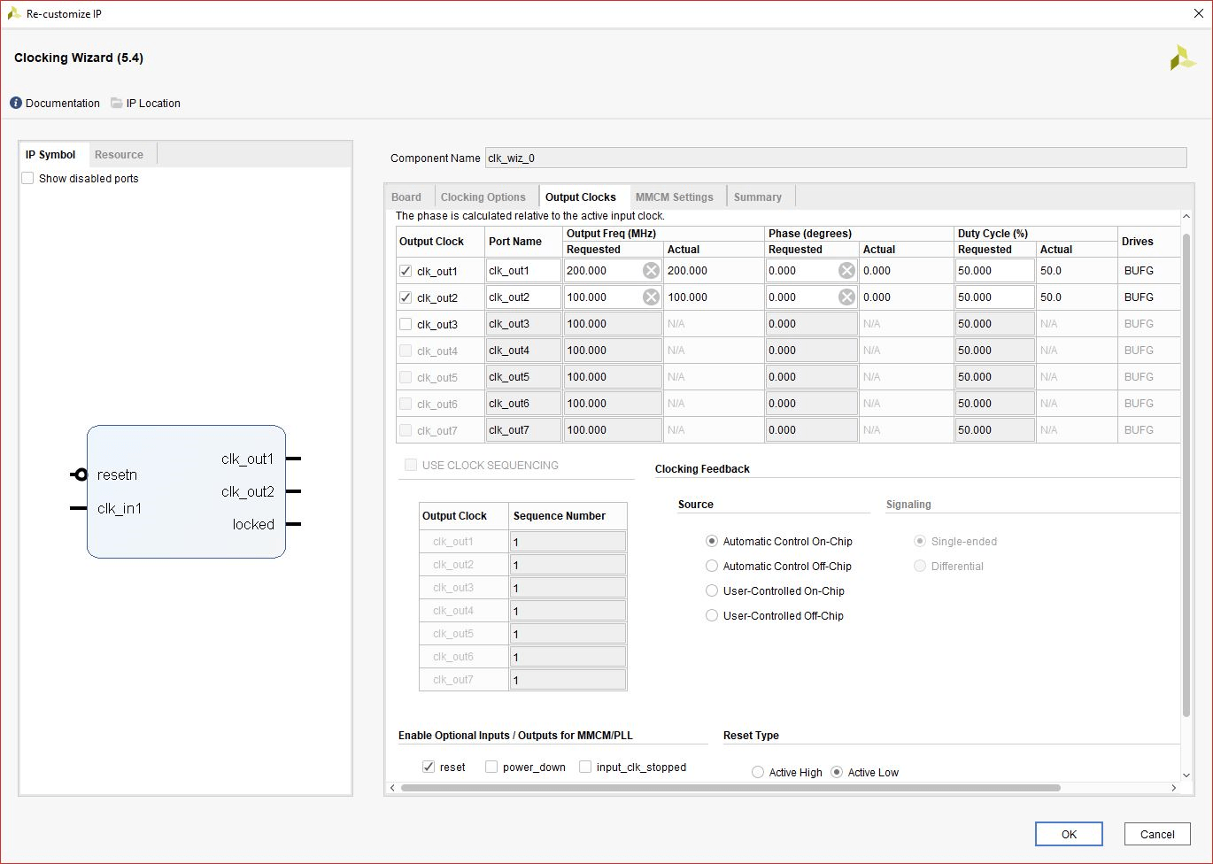
Add clocking wizard IP and in the ‘Output Clocks’, set clk_out1 frequency to 200 MHz and set clk_out2 to 100 Mhz. Select reset type as ‘active low’.
Now add the following IPs:
- AXI Ethernetlite
- AXI UARTlite
- MicroBlaze
- AXI Interrupt Controller
- AXI Timer
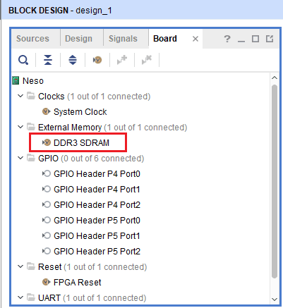
From the “Board” tab of the Block Design window, drag and drop “DDR3 SDRAM” into the block design.
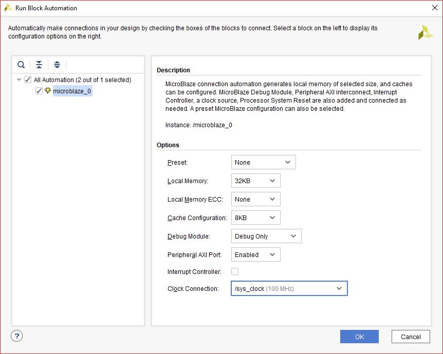
Click on ‘Run Block Automation’ and make the following changes in the MicroBlaze description window as shown
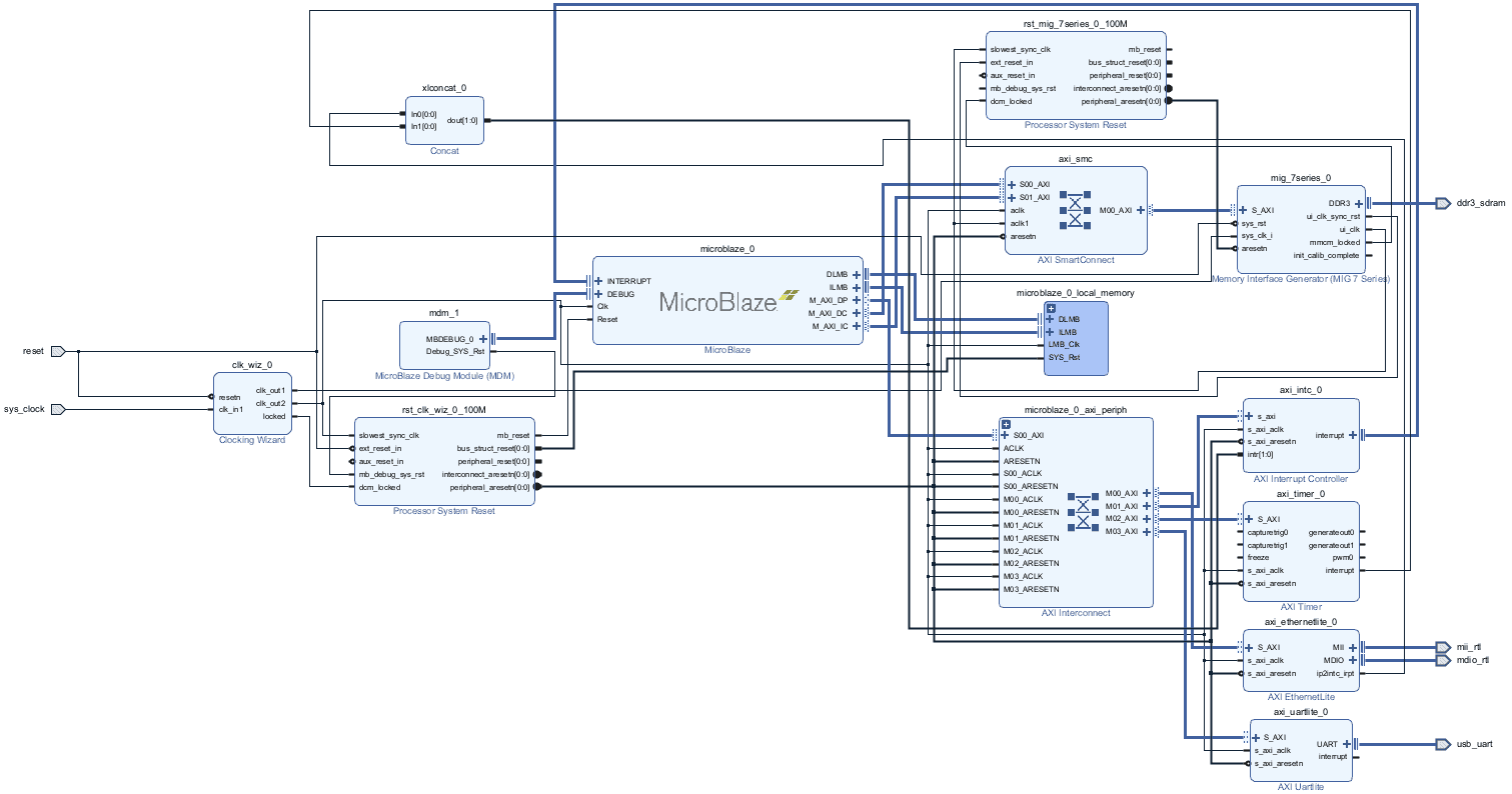
Now, click ‘Run Connection Automation’ and confirm that the final block diagram looks like this:
Step 8:
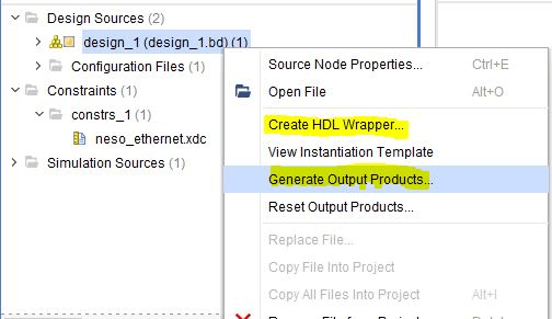
Right-click on the block design file as shown the the image below and select ‘Generate Output Products’. Similarly, select ‘Create HDL wrapper’
Step 9:
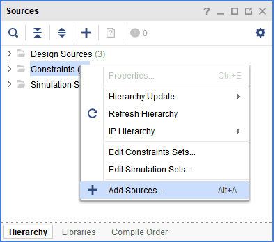
Right-click “Constraints” from the “Sources” window and select ‘Add sources’.
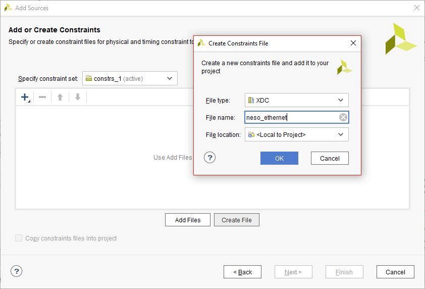
Step 10:
Click Next and then click ‘Create File’. Give a file name for the constraints file and click “Finish”.
Step 11:
Copy the following constraints to the newly created constraints file:
Step 12:
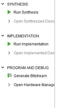
In Project Manager Tab, click ‘Run Synthesis’. If Synthesis is successful, click ‘Run Implementation’ and finally on successful implementation, select ‘Generate Bitstream’.
Step 13:
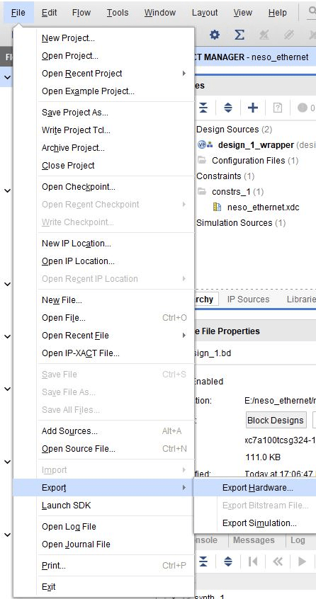
Go to File -> Export -> Export Hardware. Check ‘Include Bitstream’ and click OK.
Step 14:
Go to File -> Launch SDK. Select workspace as ‘Local to project’ and click ‘OK’ to open Xilinx SDK.
Step 15:
In SDK, Go to File -> New -> Application Project. Type in a project name, click Next and select “LwIp Echo Server” template from the list of available templates.
Step 16:
In project explorer tab, go to Xilinx -> Board Support Package Settings. Choose “lwip” in supported libraries . Select lwip library, change the “dhcp options” to “false” and “phy_link_speed” in temac_adapter_options to “CONFIG_LINKSPEED100” as shown below.
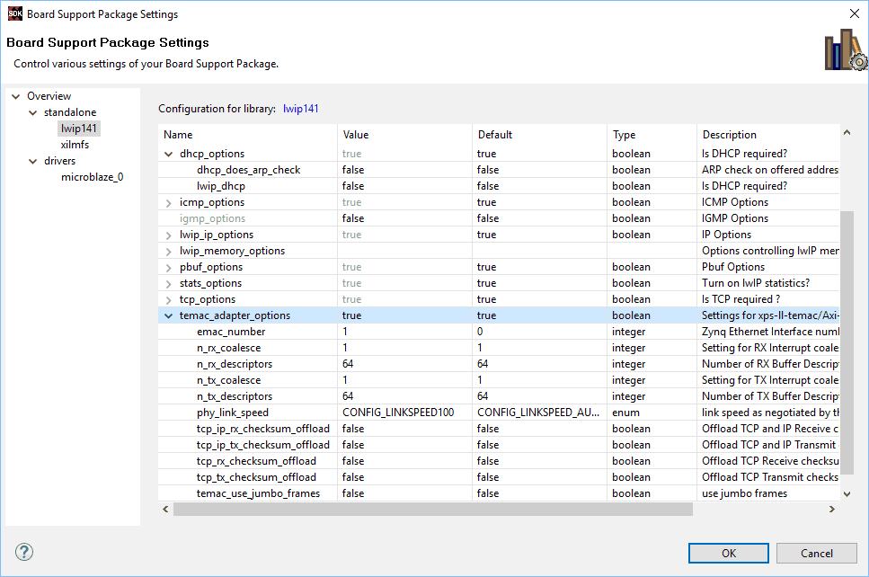
After changing the library settings, click “OK”. Once you have saved all the changes, SDK will update the BSP automatically. If that didn’t happen for any reason, run a build manually.
Step 17:
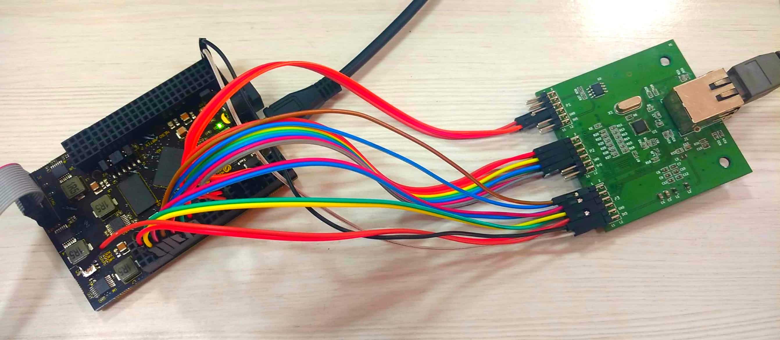
Connect Ethernet expansion module with Header P5 of Neso GPIO as per the following table:
| Expansion Module Header | Pin No. | Header P5 Pin No. | Signal Name |
|---|---|---|---|
| P1 | 5 | 11 | phy_rst_n |
| P1 | 7 | 12 | phy_col |
| P1 | 8 | 21 | phy_mdc |
| P2 | 1 | 15 | phy_crs |
| P2 | 2 | 16 | phy_mdio |
| P2 | 3 | 31 | phy_tx_clk |
| P2 | 4 | 25 | phy_rx_clk |
| P2 | 5 | 17 | phy_dv |
| P2 | 6 | 18 | phy_tx_en |
| P2 | 7 | 22 | phy_rx_data[3] |
| P2 | 8 | 32 | phy_rx_er |
| P3 | 1 | 23 | phy_rx_data[2] |
| P3 | 2 | 24 | phy_rx_data[1] |
| P3 | 3 | 26 | phy_rx_data[0] |
| P3 | 4 | 27 | phy_tx_data[0] |
| P3 | 5 | 28 | phy_tx_data[1] |
| P3 | 6 | 29 | phy_tx_data[2] |
| P3 | 7 | 30 | phy_tx_data[3] |
| P3 | 10 | 4 | GND |
| P3 | 12 | 3 | VCC |
Step 18:
Go to Xilinx -> Program FPGA and program the FPGA on Neso with a simple bootloop program.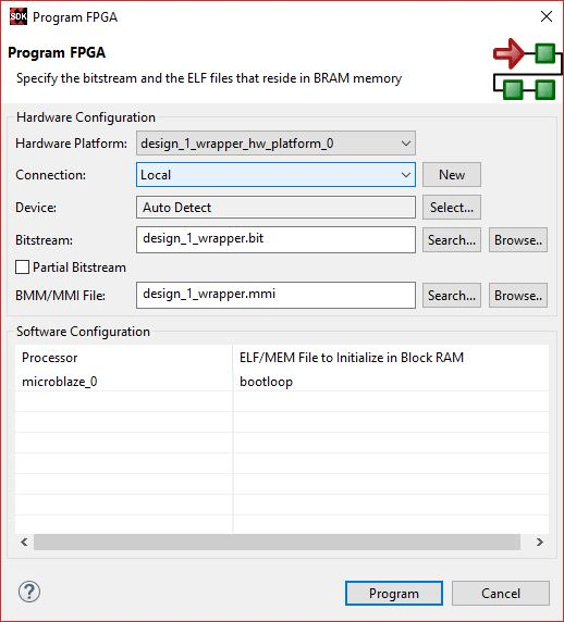
Step 19:
Open the COM port corresponding to Neso in a serial terminal with ‘9600’ baud-rate.
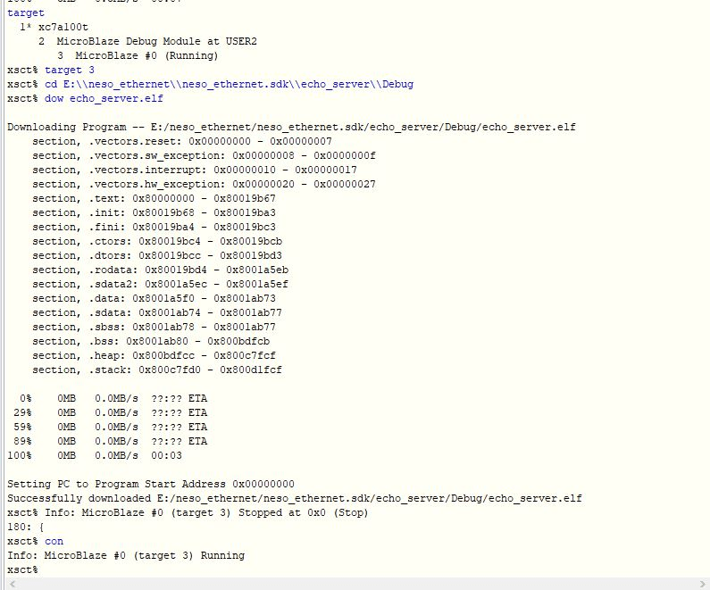
Go to Xilinx -> XSCT Console, type in a command ‘target’ it will show all the targets connected, note down the number where MicroBlaze 0 is connected (3 in this article), connect to MicroBlaze by giving the command:
target 3
Now, change to the directory where the elf file is located (..\\neso_ethernet\\neso_ethernet.sdk\\’project_name’\\Debug) by using the command:
cd E:\\neso_ethernet\\neso_ethernet.sdk\\echo_server\\Debug
Now, give the following command to run the processor:
con
Observe the details displayed on serial terminal:
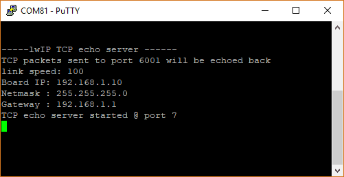
Step 20:
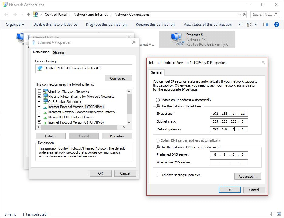
Connect Ethernet cable to expansion module and other end to PC Ethernet port, change the IPv4 address to 192.168.1.11 and default address to 192.168.1.1 in your control panel -> Network and Internet -> Network connections options. Double-click on Ethernet, select properties -> IPv4.
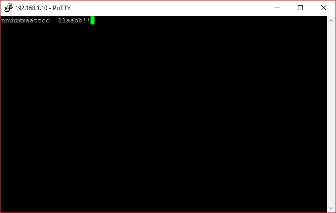
Open a telnet session with IP Address 192.168.1.10 (ip address as per main.c) at port 7, give input through keyboard and observe the output. If you enter a character from keyboard, you can observe the transmitted and echoed characters on telnet as shown.
Note: If the design does not work, try it with the lower 10 Mb/s speed. Jumper wires may create length mismatch or signal integrity issues leading to poor connection. For checking the design with 10 Mb/s, select “phy_link_speed” in temac_adapter_options as “CONFIG_LINKSPEED10” in step 15, and follow the rest of the steps.
Congratulations! You have the Ethernet working on Neso Artix 7 FPGA Module!