Onboard voltage regulators for single power rail operation
12V DC power supply
A Push Button for the reset pin
JTAG header for programming and debugging
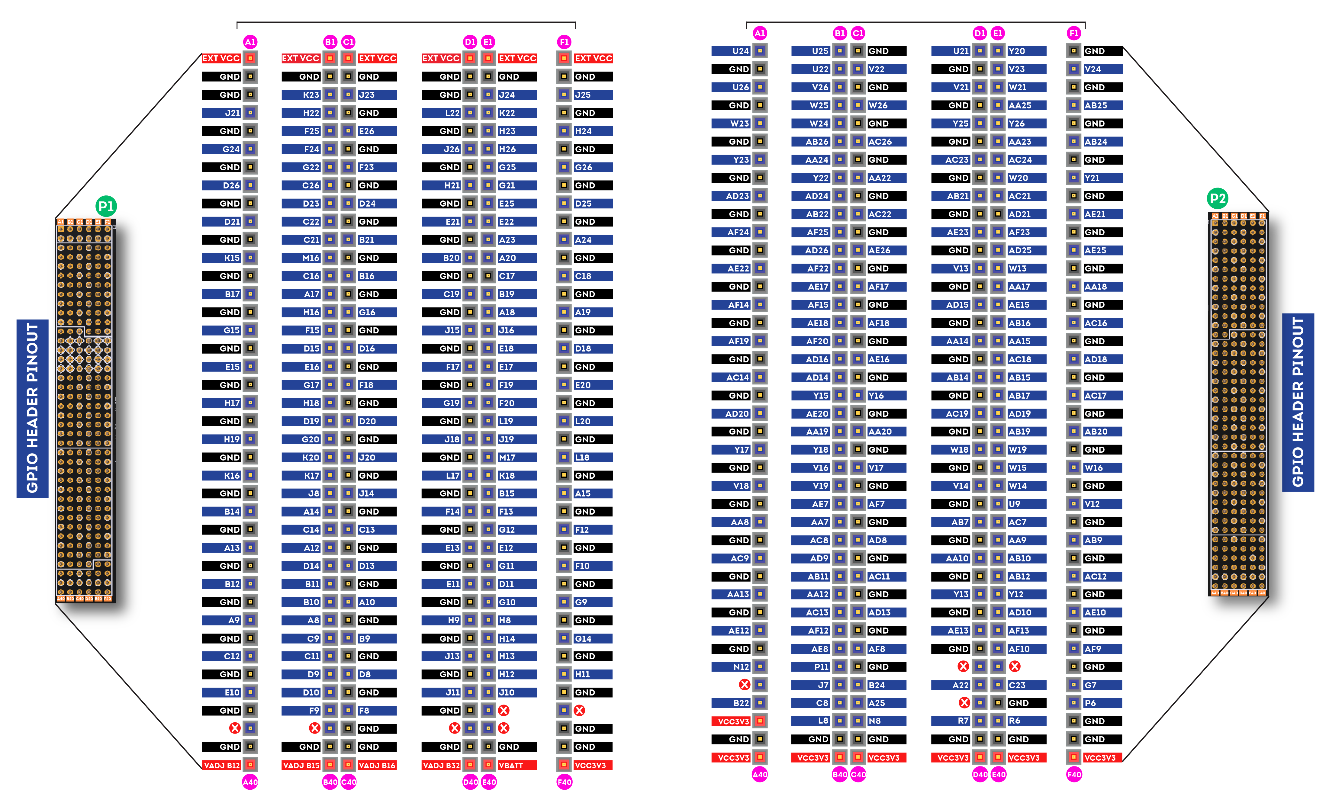
274 IOs for user-defined purposes
All user IOs are length matched and can be used as differential pairs
Callisto K7 is an easy-to-use FPGA Module featuring the AMD Kintex 7 FPGA with 4Gb DDR3 SDRAM. This board contains the AMD XC7K410T– FBG676 FPGA. The high-speed USB 3.1 interface (USB-C connector) provides a fast and easy configuration download to the onboard SPI flash. There is no need for a programmer or special downloader cable to download Bitstream to the board. The FPGA Module also provides easy access to JTAG signals on a standard Xilinx Platform Cable compatible header. Callisto K7 provides the user with the flexibility of adding their own peripherals through IO Expansion Headers.
Applications
Product Prototype Development
Communication Device Development
Accelerated Computing Integration
Development and Testing of Custom embedded processors