Introduction
Vivado Design Suite by Xilinx is used for the synthesis and analysis of HDL designs, superseding Xilinx ISE Design Suite with additional features for SoC development and high-level synthesis. This tool increases the overall productivity for designing, integrating and implementing systems with Xilinx’s UltraScale, 7 series devices, and Zynq-7000. The complete pack of Vivado Design Suite contains Vivado High-Level Synthesis, Vivado Simulator, Vivado IP Integrator, and Vivado TCL Store. In this article, we’ll be using the Vivado IP Integrator alongside the Vivado SDK to create a basic “Hello World” project for the Mimas A7 Mini FPGA Development Board. The design will contain a MicroBlaze (32-bit) soft processor and peripherals connected together by AXI bus. MicroBlaze based embedded design can use either PLB or AXI as the bus system. Since Xilinx is planning to phase out PLB and keep only AXI in the future, we will stick with AXI for our designs. More information and resources including a datasheet for MicroBlaze can be found at Xilinx’s MicroBlaze page. Advanced knowledge of MicroBlaze or AXI is not a prerequisite to follow this article. Thanks to the excellent tools provided by Xilinx, most of the design can be done without writing any code at all.
Mimas A7 Mini FPGA Development Board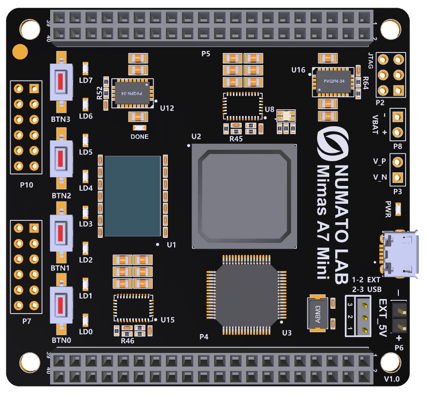
The Mimas A7 Mini is an Artix-7 based replacement and upgrade of Numato Lab’s Mimas Spartan 6 FPGA Board. Mimas A7 Mini offers a USB interface that can be used to program the board as well as to do debugging or data transfer with the host. With an XC7A35T FPGA onboard, the Mimas A7 Mini FPGA Development Board is a great choice for learning, product development, and OEM integration.
Prerequisites:
Hardware:
- Mimas A7 Mini FPGA Development Board
- (Optional) Xilinx Platform Cable USB II JTAG debugger.
- USB A to Micro USB cable
Software:
- Vivado Design Suite with SDK installed
Creating MicroBlaze based Hardware Platform for Mimas A7 Mini
The following steps will walk you through the process of creating a new project with Vivado and building a hardware platform with MicroBlaze soft processor using an IP integrator. Numato Lab’s Mimas Artix 7 Mini FPGA Development Board is used in this example but any compatible FPGA platform can be used with minor changes to the steps. Screenshots are added wherever possible to make the process easier for the reader.
Step 1:
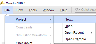
Launch Vivado Design Suite, go to “File->Project->New” to create a new project. The “New project” wizard will pop up. Click “Next” to continue.
Step 2:
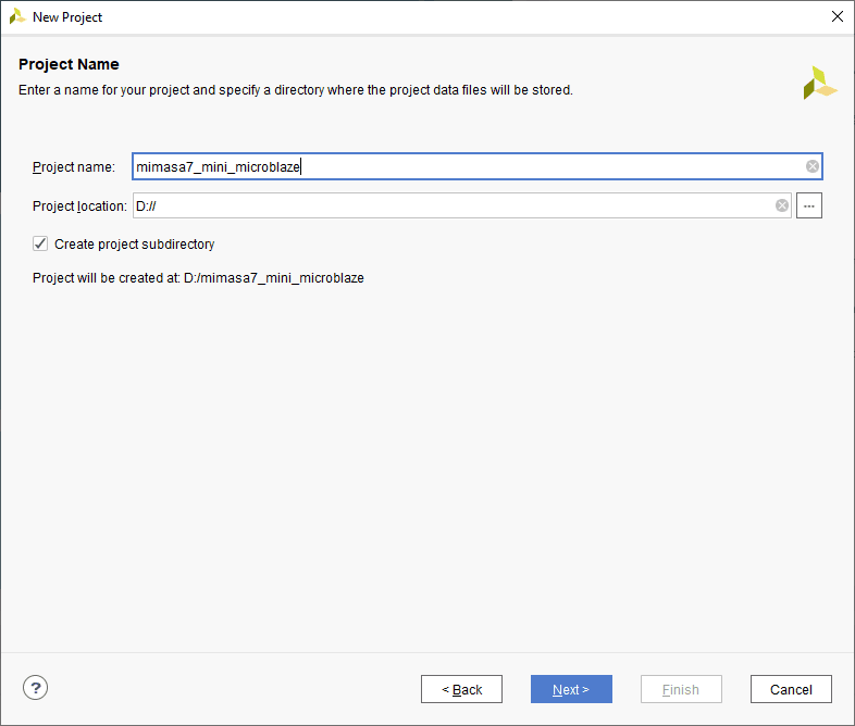
In the “Project Name” wizard, type in a name for the project and save it at a convenient location. For this example, we shall use “mimasa7_mini_microblaze” as the project name (feel free to use any name). Select the checkbox below to keep all project files in a single folder. Click “Next” to proceed.
Step 3:
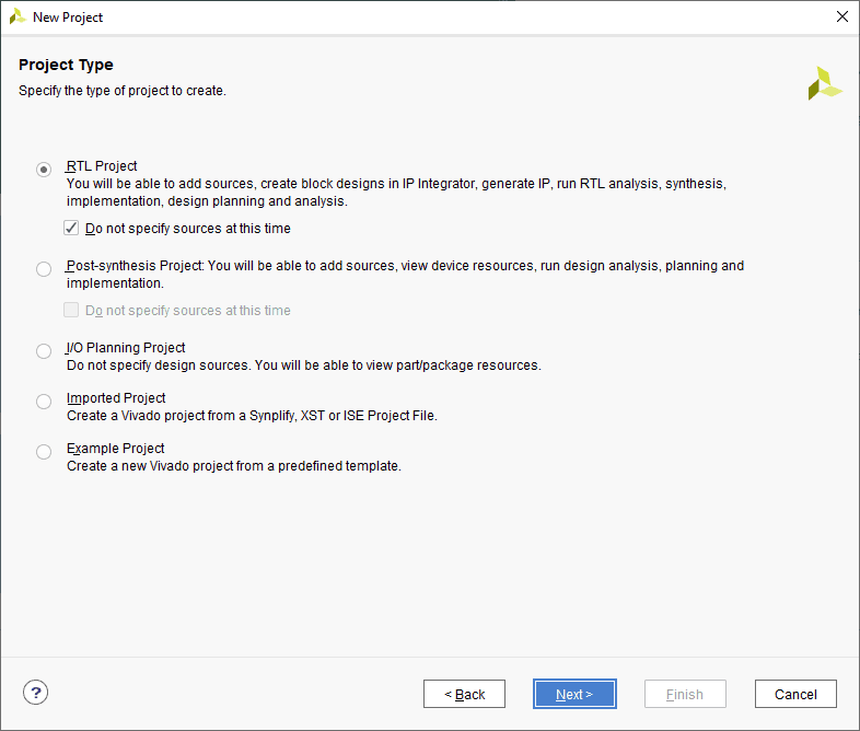
In the “Project type” wizard, select “RTL Project” and select the checkbox to skip specifying the source at the moment. Click “Next”.
Step 4:
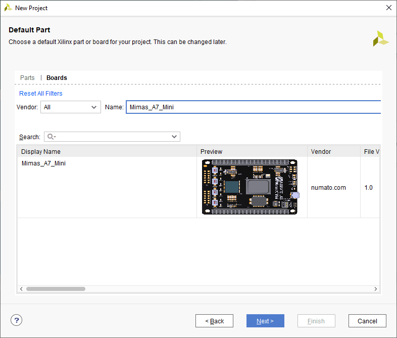
At the “Default Part” wizard, select “Boards” and then select “Mimas_A7_Mini” board. Click “Next” to continue. If Mimas_A7_Mini is not displayed in the Boards list, you need to install Mimas_A7_Mini board support files appropriately and retry this step. You can download Mimas A7 Mini board support files for Vivado here. Follow the readme in the link on how to install the Vivado board files in your system.
In the next wizard, click “Finish” to create a new project. When the new project wizard exits, a new project will open up in Vivado with the selected settings.
Step 5:
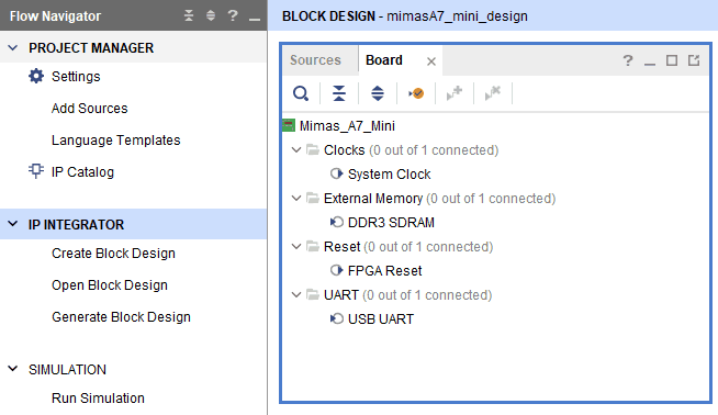
In the “Flow Navigator” panel, select “Create Block Design” under the IP integrator section. Give an appropriate name (Eg: “mimasa7_mini_design”) to the design and click “OK”. Select “Board” in the “Block Design” block. The default peripherals available for Mimas A7 Mini Board will be displayed.
Step 6:
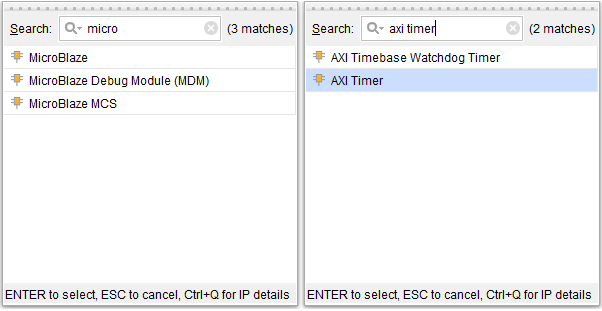
Add System Clock, DDR3 SDRAM and USB UART to the design by double-clicking the corresponding peripherals. In the Diagram window, right-click and select “Add IP” from the popup menu. Search for “MicroBlaze” & “AXI Timer” and add them to the design by double-clicking them.
Step 7:
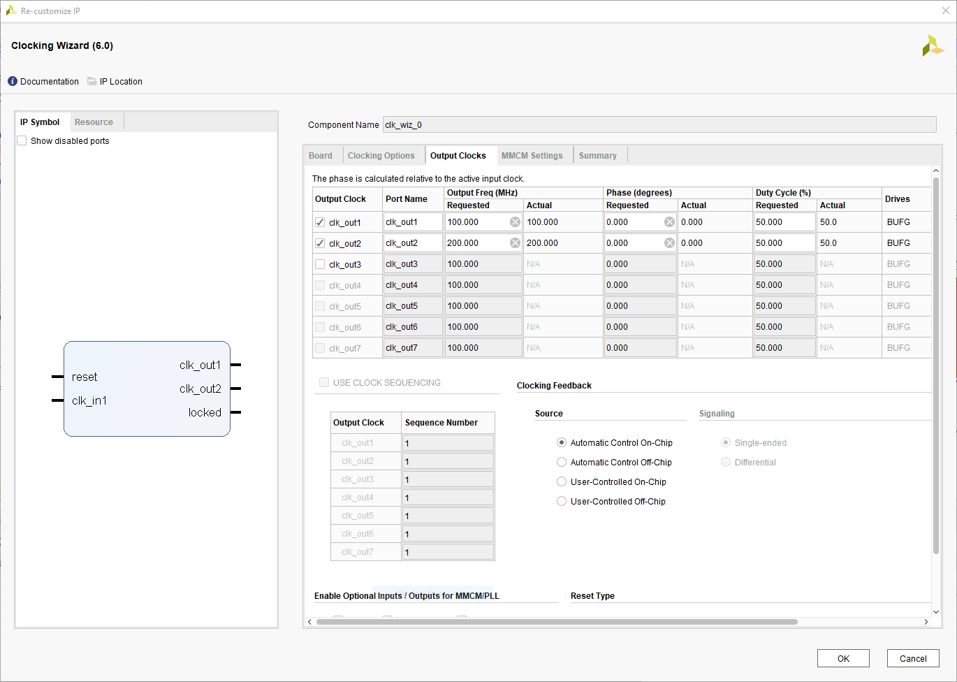
Double click “Clocking Wizard” IP and customize “Output Clocks” settings as shown in the following image.
Step 8
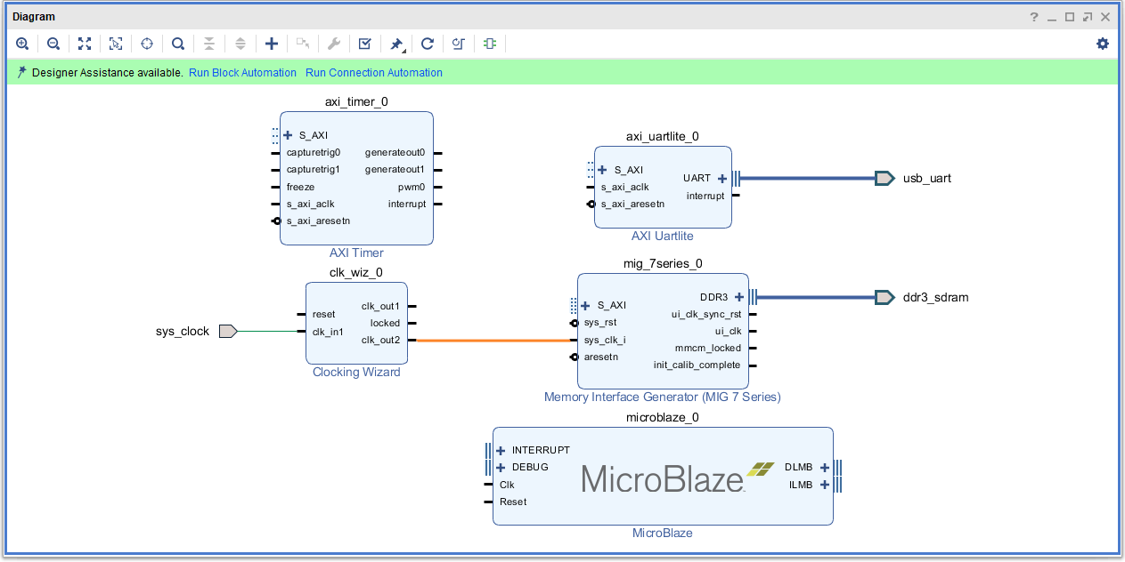
Remove existing ‘sys_clk_i’ connection and input port (if any) and connect ‘clk_out2‘ net on the clocking Wizard to ‘sys_clk_i’ of ‘MIG 7 Series’ block as shown in the following image.
Step 9:
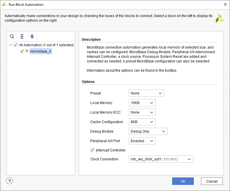
Click “Run Block Automation” present in the “Designer Assistance available” bar on the top left corner of the window to complete the design. Select the settings as shown in the following image. Click “OK” for Vivado to automatically configure the blocks for you. Once Block Automation is complete, run “Connection Automation” so Vivado can connect the blocks together to make a complete system.
Step 10:
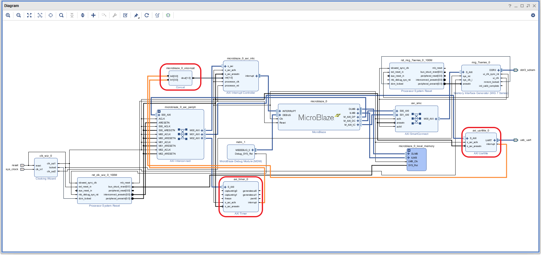
Connect interrupt output lines from “AXI Timer” and “UARTLite” to the “Concat” block as shown in below figure. Select “Validate Design” option from the Tools menu to make sure that connections are correct.
Step 11:
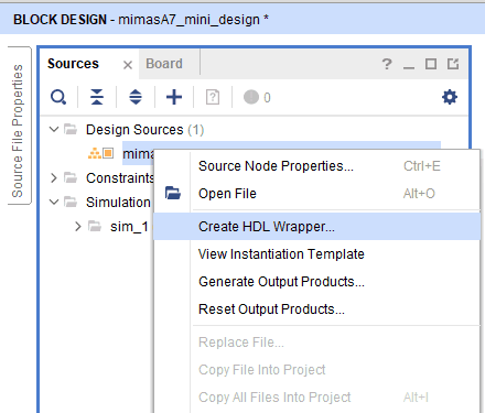
Right-click “mimasA7_mini_design” in the “Sources” window, select “Create HDL Wrapper” from the popup menu. Click “OK” on the window that appears to finish generating a wrapper.
Step 12:
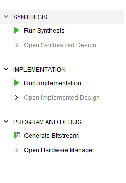
Click “Generate Bitstream” under the “Program And Debug” section to synthesize, implement and generate a bitstream.
Step 13:
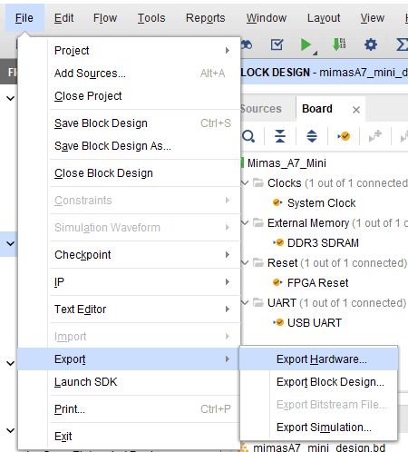
Once the implementation and generation of the bitstream are successfully completed, we need to export the hardware along with bitstream. Go to the “File” menu, select “Export->Export Hardware”. Select the “Include bitstream” checkbox and click “OK” in the “Export Hardware” wizard.
Step 14:
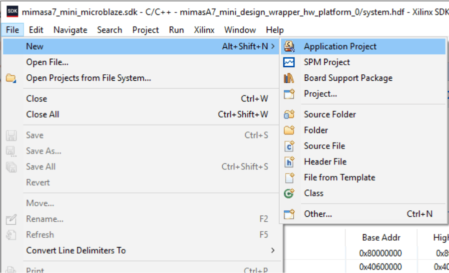
Launch SDK from the File menu. You may choose to use the local project directory as SDK workspace or select another directory if appropriate. Once the SDK window appears, select “New->Application Project” from the “File” menu. Type in a project name and click “Next” to select the “Hello World” template from the list.
Step 15:
Once the project is created, the SDK will automatically run a build. If that didn’t happen for any reason, run a build manually. Once the build is completed successfully, power up the Mimas A7 Mini FPGA Development Board and connect the Xilinx Platform USB cable and Micro USB cable for Serial debugging to the board.
Step 16:
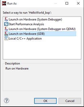
Program the board by selecting “Program FPGA” under “Xilinx” menu. Open the serial port corresponding to Mimas A7 Mini on your operating system using your preferred Serial Terminal software such as HyperTerminal, PuTTY, Tera Term, etc. Now run the application by selecting the .elf file from the project hierarchy and then click the Run icon on the main toolbar. Select “Launch On Hardware (GDB)” when asked as shown in the image below.
If everything went well, the application running on the board should print “Hello World” over the USB UART and should be displayed on the Serial Terminal application.
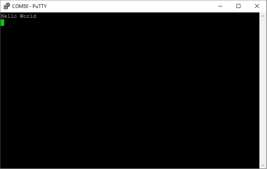
And that’s all folks, you’ve successfully created your first “Hello World” project on the Mimas A7 Mini.