Introduction
The purpose of this article is to help readers understand how to use DDR3 memory available on Telesto using Intel DDR3 UniPHY IP Core easily. The Intel DDR3 UniPHY IP core for MAX 10 devices provides users with a simple Avalon-MM interface for interacting with DDR3, abstracting all the complexities of controlling a DDR3 memory. This article will demonstrate how to write to the DDR3 memory on Telesto MAX10 FPGA Module using simple Verilog code and then read back the data. The design will compare the data written to DDR3 and the data read back from it. The verification results and DDR3 calibration results are indicated using GPIO pins on Telesto GPIO header P4.
Prerequisites
- Hardware:
- Telesto MAX10 FPGA Module
- Intel USB-Blaster II JTAG probe (optional)
- USB A to Micro B Cable
- Software:
- Quartus software 17.0 or newer
Let’s get started
The following steps will walk you through the process of creating a simple DDR3 project for Telesto using Quartus.
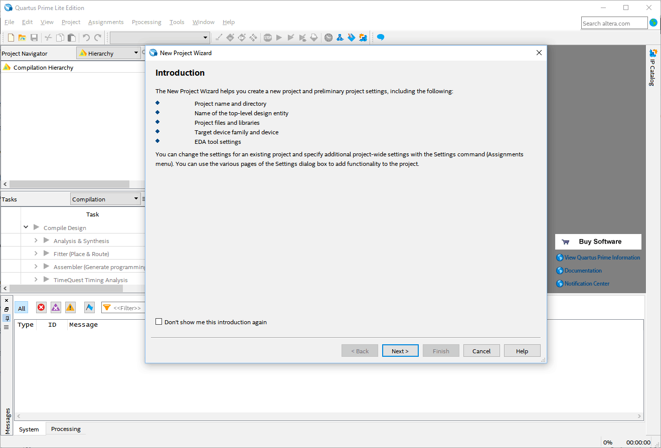
Step 1:
Open Quartus software and select “File” -> “New Project Wizard” from the menu bar. A “New Project Wizard” dialog will open. Click “Next” to proceed.
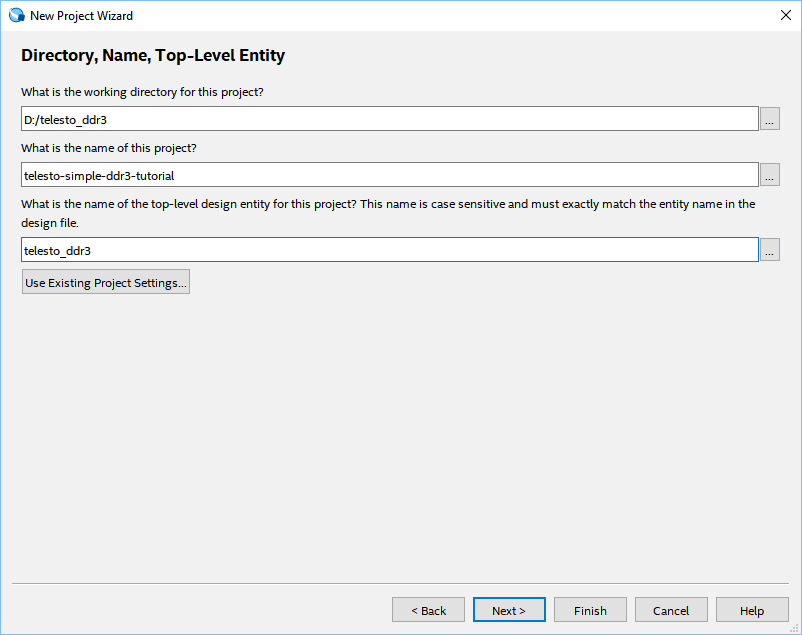
Step 2:
Enter a name for the project and select a convenient project location and top-level entity name. For this article, author used “telesto-simple-ddr3-tutorial” as the project name and “telesto_ddr3” as the top-level entity name.
Step 3:
Go to the “Family, Device & Board settings” tab by clicking “Next” for three consecutive times. Select the Device (10M16DAF484C8G or 10M50DAF484C8G as per your Telesto variant) as shown below and click “Next” to proceed.
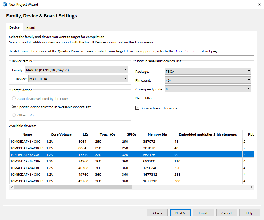
Click “Next” and “Finish” to create a new project.
Step 4:
Double-click on “DDR3 SDRAM Controller with UniPHY” IP Core from IP Catalog (View -> Utility Windows -> IP Catalog), “Save IP Variation” window will open. Enter the IP Variation file name and click “OK”. The “DDR3 SDRAM Controller with UniPHY” configuration window will open. Change the “PHY Settings” as shown below
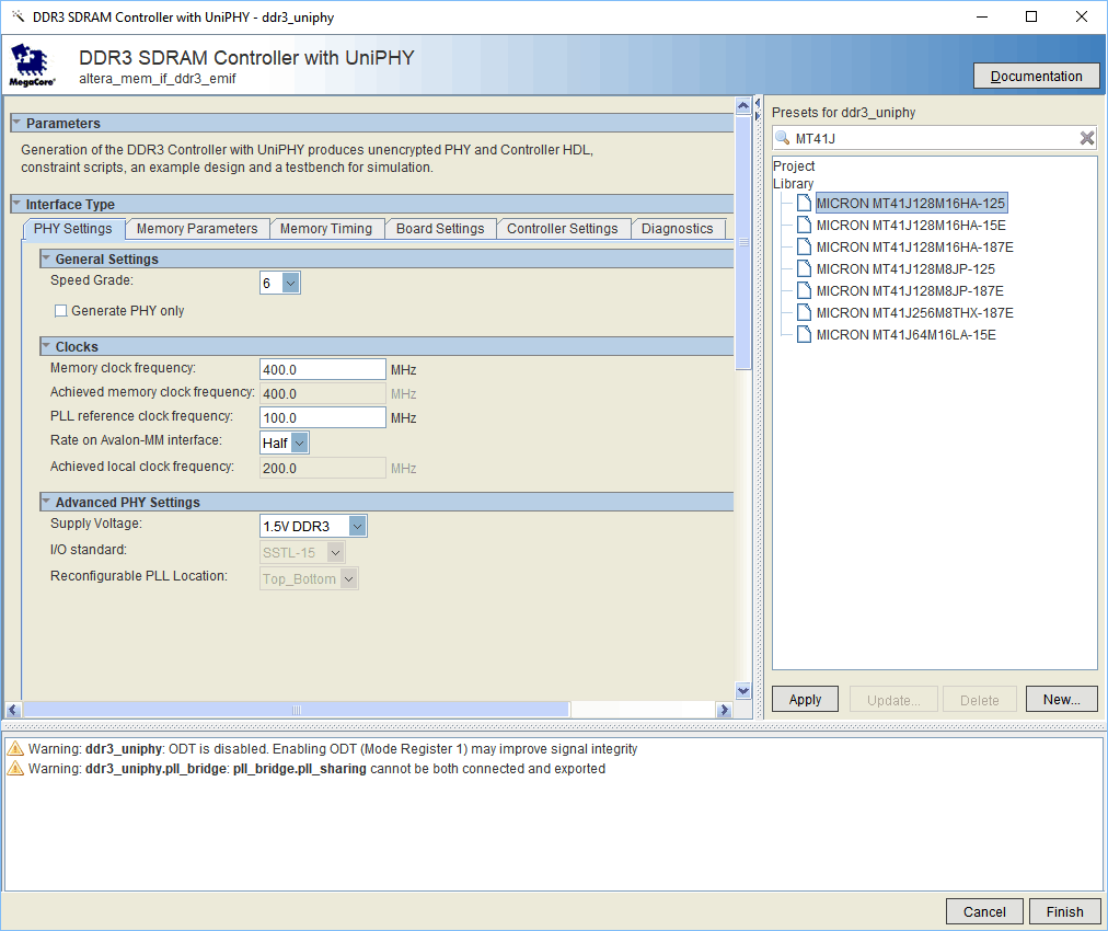
Search for the memory part number “MT41J128M16HA-125” and click “Apply” to change the “Memory Parameters”. Go to Memory Parameters tab and change the “ODT Rtt nominal value” to “RZQ/4”. In “Controller Settings” tab, select the “Maximum Avalon-MM burst length” to 64. Click “Finish” to generate DDR3 UniPHY IP Core. Select/de-select the “Generate Example Design” and click “Generate”. Once the IP core generated successfully, click “Exit” and “Yes” to add IP files to the project.
Step 5:
Create a Verilog HDL File with .v extension and copy-paste the following code in telesto_ddr3.v. Change the DDR3 UniPHY instantiation name as per IP Variation file name you gave in Step 4.
The RTL code instantiates the DDR3 SDRAM UniPHY IP core along with its own user interface logic for interfacing with the DDR3 memory controller. The input clock for DDR3 UniPHY IP comes directly from the Telesto’s 100 MHz onboard oscillator.
A simple FSM is implemented with five states to interface with the memory controller. The states are IDLE, WRITE, RD_CMD, READ and PARK. Initially, the state machine is in IDLE state.
IDLE: In this state, the FSM waits for the memory calibration to complete. When the calibration completes successfully (led_calib_success goes HIGH) the state machine changes to WRITE state.
WRITE: In this state, the state machine waits for the ready signal (avl_ready) which is asserted by the memory controller to accept the write command and data requests. Once the DDR3 controller asserts the avl_ready signal, the core is ready to accept the commands and data requests. The state machine writes the command and data to the memory controller and changes its state to RD_CMD.
RD_CMD: In this state, the state machine de-asserts the write request (avl_write_req) & burst begin (avl_burstbegin) signals and waits for the ready signal (avl_ready) which is asserted by the memory controller to accept the read command request. Once the DDR3 controller asserts the avl_ready signal, the core is ready to accept the read command request. The state machine writes the read command to the DDR3 UniPHY IP core and changes its state to READ.
READ: The state machine de-asserts the read request (av_read_req) & burst begin (avl_burstbegin) signals and waits for the read data valid (avl_rdata_valid) signal from memory controller. Whenever the DDR3 controller asserts avl_rdata_valid signal, the state machine reads back the data from memory to data_read_from_memory register and changes its state to PARK.
PARK: In this state, the state machine compares the data written to memory and the data read back from memory. If the data match, led_pass goes HIGH otherwise led_fail goes HIGH.
module telesto_ddr3 (
 input  clk_in,
 output [13:0] mem_a,
 output [2:0]  mem_ba,
 inout  [0:0]  mem_ck,
 inout  [0:0]  mem_ck_n,
 output [0:0]  mem_cke,
 output [0:0]  mem_cs_n,
 output [1:0]  mem_dm,
 output [0:0]  mem_ras_n,
 output [0:0]  mem_cas_n,
 output [0:0]  mem_we_n,
 output mem_reset_n,
 inout  [15:0] mem_dq,
 inout  [1:0]  mem_dqs,
 inout  [1:0]  mem_dqs_n,
 output [0:0]  mem_odt,
 output led_calib_success,
 output led_calib_fail,
 output reg led_pass,
 output reg led_fail
 );

wire local_init_done;
wire afi_reset_n;
wire afi_clk;
wire avl_ready;
reg  avl_burstbegin;
wire avl_rdata_valid;
reg  avl_read_req;
reg  avl_write_req;
reg  [24:0] avl_addr;
wire [63:0] avl_rdata;
reg  [63:0] avl_wdata;
wire [7:0]  avl_be;
reg  [7:0]  avl_size;

reg [2:0] state;
reg [63:0]data_to_write = {32'hAA55AA55, 32'h55AA55AA};
reg [63:0]data_read_from_memory = 64'd0;

// Power-on-reset generator circuit.
// Asserts resetn for 1023 cycles, then deasserts
// `resetn` is Active low reset
reg [9:0] por_counter = 1023;
always @ (posedge clk_in) begin
 if (por_counter) begin
 por_counter <= por_counter - 1 ;
 end
end

wire resetn = (por_counter == 0);

// DDR3 UniPHY instantiation
ddr3_uniphy telesto_ddr_inst (
 .pll_ref_clk    (clk_in),
 .global_reset_n (resetn),
 .soft_reset_n   (resetn),
 .afi_clk        (afi_clk),
 .afi_half_clk   (),
 .afi_reset_n    (afi_reset_n),
 .afi_reset_export_n (),
 .mem_a          (mem_a),
 .mem_ba         (mem_ba),
 .mem_ck         (mem_ck),
 .mem_ck_n       (mem_ck_n),
 .mem_cke        (mem_cke),
 .mem_cs_n       (mem_cs_n),
 .mem_dm         (mem_dm),
 .mem_ras_n      (mem_ras_n),
 .mem_cas_n      (mem_cas_n),
 .mem_we_n       (mem_we_n),
 .mem_reset_n    (mem_reset_n),
 .mem_dq         (mem_dq),
 .mem_dqs        (mem_dqs),
 .mem_dqs_n      (mem_dqs_n),
 .mem_odt        (mem_odt),
 .avl_ready      (avl_ready),
 .avl_burstbegin (avl_burstbegin),
 .avl_addr       (avl_addr),
 .avl_rdata_valid(avl_rdata_valid),
 .avl_rdata      (avl_rdata),
 .avl_wdata      (avl_wdata),
 .avl_be         (avl_be),
 .avl_read_req   (avl_read_req),
 .avl_write_req  (avl_write_req),
 .avl_size       (avl_size),
 .local_init_done(local_init_done),
 .local_cal_success (led_calib_success),
 .local_cal_fail (led_calib_fail),
 .pll_mem_clk    (),
 .pll_write_clk  (),
 .pll_locked     (),
 .pll_capture0_clk (),
 .pll_capture1_clk ()
 );


//**************** State Machine start here ******************//

assign avl_be = 8'hff;

localparam IDLE      = 3'h0,
           WRITE     = 3'h1,
           RD_CMD    = 3'h2,
           READ      = 3'h3,
           PARK      = 3'h4;

always@(posedge afi_clk)
begin
  if(~afi_reset_n) begin
    state         <= IDLE;
    avl_burstbegin<= 1'b0;
    avl_size      <= 0;
    avl_addr      <= 0;
    avl_write_req <= 1'b0;
    avl_read_req  <= 1'b0;
    led_pass      <= 1'b0;
    led_fail      <= 1'b0;
  end
  else begin
    case(state)
      IDLE : begin
         if(led_calib_success) begin
           state <= WRITE;
         end
      end

      WRITE : begin
         if(avl_ready) begin
           avl_write_req <= 1'b1;
           avl_size      <= 1;
           avl_addr      <= 0;
           avl_wdata     <= data_to_write;
           state         <= RD_CMD ;
           avl_burstbegin<= 1'b1;
         end
      end

      RD_CMD : begin
         avl_burstbegin<= 1'b0;
         avl_write_req <= 1'b0;
         if(avl_ready) begin
           avl_read_req  <= 1'b1;
           avl_burstbegin<= 1'b1;
           avl_addr      <= 0;
           avl_size      <= 1;
           state         <= READ;
         end
      end

      READ: begin
         avl_read_req   <= 1'b0;
         avl_burstbegin <= 1'b0;
         if(avl_rdata_valid) begin
           data_read_from_memory <= avl_rdata;
           state <= PARK;
         end
      end

      PARK : begin
         if (data_to_write == data_read_from_memory) begin
           led_pass <= 1'b1;
         end else if (data_to_write != data_read_from_memory) begin
           led_fail <= 1'b1;
         end
      end

      default : state <= IDLE;
    endcase
  end
end
endmodule
Step 6:
To assign constraints, save the telesto_ddr3_constraints.tcl to the project location and run using Tcl Scripts. Run the “Analysis & Synthesis” from Processing menu (Processing -> Start -> Start Analysis & Synthesis). When Analysis & Synthesis is completed, go to “Tools -> Tcl Scripts” and run the files “<IP Variation name>_p0_pin_assignments.tcl” followed by “telesto_ddr3_constraints.tcl“. Open “Assignment Editor” or “Pin Planner” to verify the pin assignments. Finally, generate the bitstream by clicking on the “Start Compilation” from the “Processing” menu or just click “CTRL+ L”.
Step 7:
Once the bitstream is generated successfully, power up the Telesto and program it with the generated bitstream.
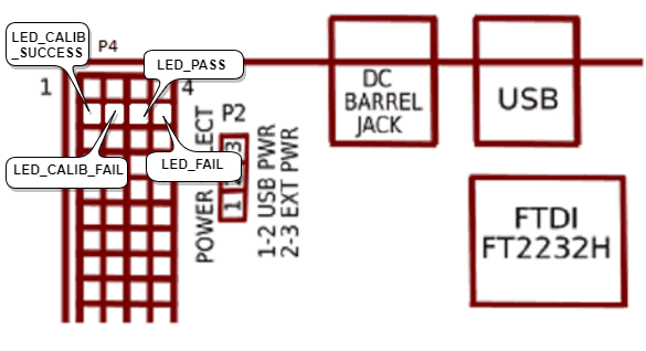
The 2nd row pins of GPIO Header P4 of Telesto are used for led_calib_success, led_calib_fail, led_pass and led_fail signals respectively. Those pins are connected to MAX 10 FPGA pins AA1, AA2, Y1 and Y2 respectively. After programming make sure that led_calib_success (calibration done) signal goes HIGH indicating that initial calibration completed successfully. The led_calib_fail signal should stay LOW as led_calib_fail being HIGH indicates initial calibration failed. The led_pass signal should be HIGH indicating that data was written to memory and read back successfully and led_fail should be LOW as led_fail HIGH indicates failed attempt to write and read data from memory. The below picture illustrates the calibration and status signals on the Telesto MAX10 FPGA Module GPIO header P4.
You can use either LED in series with a resistor or a multimeter to check the output of led_calib_success, led_calib_fail, led_pass and led_fail signals. If you observe led_calib_success and led_pass signals HIGH and led_fail and led_calib_fail signals LOW, then your Telesto MAX10 DDR3 example design worked. Congratulations!