Introduction
Telesto is an easy to use FPGA Module featuring Intel (formerly Altera) MAX 10 FPGA. The MAX 10 FPGAs come with dual embedded NOR Flash, with almost instant-on functionality hence eliminating the need for external configuration memory. The dual configuration flash on MAX 10 allows users to store and dynamically switch between two bitstreams on a single chip. They also feature integrated Analog-to-Digital Converters (ADCs). Telesto is pin compatible with Saturn Spartan 6 FPGA Module, Neso Artix 7 FPGA Module , Skoll Kintex 7 FPGA Module as well as Styx Zynq FPGA Module and offers a seamless upgrade path. The high speed USB 2.0 provides fast and easy configuration download to the built-in flash via JTAG using OpenOCD. No programmer or special downloader cable is needed to download the bitstream to the board. Telesto provides users with flexibility in adding their own peripherals through IOs available on its headers.
Board Features
- Pin compatible with Saturn Spartan 6 FPGA Module, Neso Artix 7 FPGA Module, Skoll Kintex 7 FPGA Module and Styx Zynq FPGA Module and offers a seamless upgrade path
- Device: MAX 10 FPGA (10M16DA or 10M50DA, F484 package and Speed Grade: -C8)
- DDR3: 2Gb DDR3 (MT41J128M16HA-125:K or equivalant)
- Internal Flash Memory
- 100MHz LVDS oscillator
- High Speed USB 2.0 interface. FT2232H Channel A can be used for custom applications. Channel B is connected to MAX 10 JTAG.
- Onboard voltage regulators for single power rail operation
- FPGA configuration via external JTAG and USB
- Maximum IOs for user-defined purposes
- FPGA – 150 IOs
- Analog Inputs – 8 IOs
Applications
- Product Prototype Development
- Accelerated computing integration
- Development and testing of custom embedded processors
- Signal Processing
- Communication devices development
- Educational tool for Schools and Universities
- System monitoring
How to Use Telesto MAX10 FPGA Module
The following sections describe in detail how to use this module.
Hardware Accessories Required
Along with the module, you may need the items in the list below for easy and fast installation.
- USB A to Micro B cable.
- USB-Blaster II (JTAG programmer, Optional)
- DC Power supply (Optional)
Connection Diagram
This diagram should be used as a reference only. For detailed information, see Telesto’s schematics and mechanical dimensions at the end of this page. Details of individual connectors are as below.
USB Interface
The on board full speed USB controller helps a PC/Linux/Mac computer to communicate with this module. Use a USB A to Micro B cable to connect to  a PC. By default, the module is powered by USB so make sure not to overcrowd unpowered USB hubs (the picture on the right shows USB Micro connector).
DC Power Supply
By default, the board is configured to use +5V supply from USB. So an external power is not required unless USB port is unable 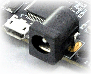 to supply enough current. USB 2.0 ports are only capable of providing enough current for the module for small designs which require less power. The current requirement for this board largely depends on your application. Please consult FPGA data sheet for more details on power requirements. If for any reason, an external power supply needs to be used for the board, the Power select jumper should be configured properly before connecting the power supply. Please refer to the marking on the board for more details. The external power supply should be in the range of +5 to +12V, with sufficient current rating.
Power Select
The “Power Select” header P2 is used to configure the power source for the board. Connect pins 1 and 2 to use USB power and connect pins 2 and 3 to use the external DC power.
Configuration Switch and Reset Button
Telesto features a DIP-Switches and Push-Button as shown below
| Switch | Pin Name |
|---|---|
| DIP-Switch (SW1) | |
| 1 | nCONFIG |
| 2 | CONFIG_SEL |
DIP-Switches:
DIP Switches are connected to FPGA pins H9 (nCONFIG) and H10 (CONFIG_SEL). nCONFIG and CONFIG_SEL pins are pulled up with 10K resistor.
nCONFIG is used to control the configuration cycle. ON to OFF transition will reset the FPGA and OFF to ON transition will trigger the FPGA configuration.
CONFIG_SEL pin is used to select the image to load the configuration. The image CFM0 is selected when this pin is OFF state and image CFM1 is selected when this pin is ON state. CFM0 and CFM1 are internal flash configuration images.
Reset Push-Button:
Telesto features a Push-button S1 normally meant to be used as “Reset” signal for designs running on FPGA. Push button S1 is connected to FPGA pin D9. Push-button S1 is active-high, and users need to enable FPGA’s internal Pulldown on the pin D9 to use the pushbutton correctly. This pushbutton can also be used for any other input, and is not just limited to be used as a Reset signal.
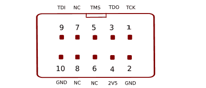
JTAG
JTAG connector provides access to FPGA’s JTAG pins. A USB-Blaster II cable can be used to for JTAG programming.
GPIOs
This device is equipped with a maximum 150 user IO pins that can be used for various custom applications. All user IOs are length matched and can be used as differential pairs.
Bank wise IO Length Matching Details:
| IO Bank | Length |
|---|---|
| Bank 2 IOs length matched to | 1740 mils |
| Bank 3 IOs length matched to | 1520 mils |
| Bank 4 IOs length matched to | 1520 mils |
| Bank 7 IOs length matched to | 1520 mils |
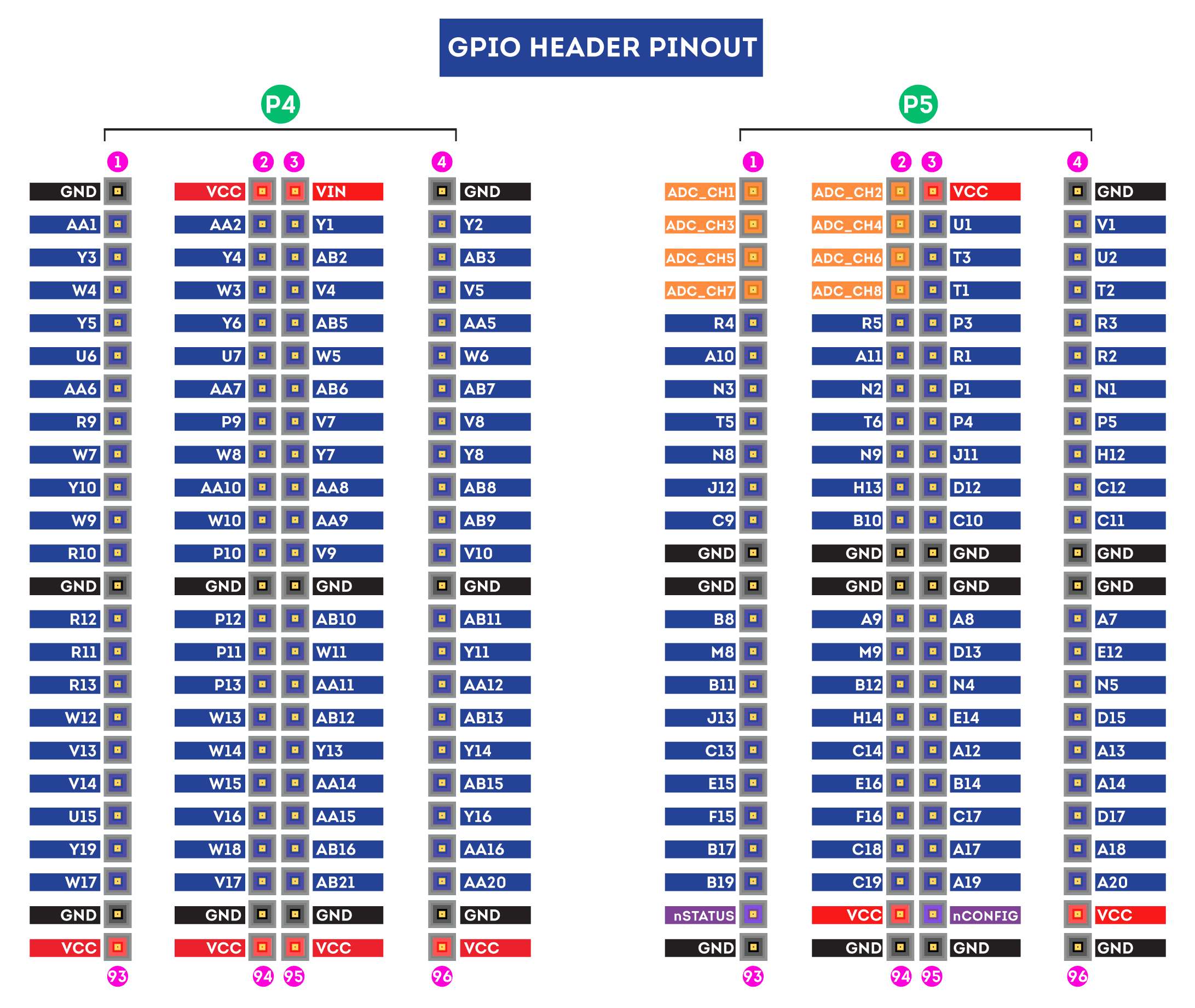
Header P4
| Pin No. On The Header | 10M50DA (F484) Pin No. | Pin No. On The Header | 10M50DA (F484) Pin No. |
|---|---|---|---|
| 1 | GND | 2 | VCC3V3 |
| 3 | VIN | 4 | GND |
| 5 | AA1 | 6 | AA2 |
| 7 | Y1 | 8 | Y2 |
| 9 | Y3 | 10 | Y4 |
| 11 | AB2 | 12 | AB3 |
| 13 | W4 | 14 | W3 |
| 15 | V4 | 16 | V5 |
| 17 | Y5 | 18 | Y6 |
| 19 | AB5 | 20 | AA5 |
| 21 | U6 | 22 | U7 |
| 23 | W5 | 24 | W6 |
| 25 | AA6 | 26 | AA7 |
| 27 | AB6 | 28 | AB7 |
| 29 | R9 | 30 | P9 |
| 31 | V7 | 32 | V8 |
| 33 | W7 | 34 | W8 |
| 35 | Y7 | 36 | Y8 |
| 37 | Y10 | 38 | AA10 |
| 39 | AA8 | 40 | AB8 |
| 41 | W9 | 42 | W10 |
| 43 | AA9 | 44 | AB9 |
| 45 | R10 | 46 | P10 |
| 47 | V9 | 48 | V10 |
| 49 | GND | 50 | GND |
| 51 | GND | 52 | GND |
| 53 | R12 | 54 | P12 |
| 55 | AB10 | 56 | AB11 |
| 57 | R11 | 58 | P11 |
| 59 | W11 | 60 | Y11 |
| 61 | R13 | 62 | P13 |
| 63 | AA11 | 64 | AA12 |
| 65 | W12 | 66 | W13 |
| 67 | AB12 | 68 | AB13 |
| 69 | V13 | 70 | W14 |
| 71 | Y13 | 72 | Y14 |
| 73 | V14 | 74 | W15 |
| 75 | AA14 | 76 | AB15 |
| 77 | U15 | 78 | V16 |
| 79 | AA15 | 80 | Y16 |
| 81 | Y19 | 82 | W18 |
| 83 | AB16 | 84 | AA16 |
| 85 | W17 | 86 | V17 |
| 87 | AB21 | 88 | AA20 |
| 89 | GND | 90 | GND |
| 91 | GND | 92 | GND |
| 93 | VCC3V3 | 94 | VCC3V3 |
| 95 | VCC3V3 | 96 | VCC3V3 |
Header P5
| Pin No. On The Header | 10M50DA (F484) Pin No. | Pin No. On The Header | 10M50DA (F484) Pin No. |
|---|---|---|---|
| 1 | ADC_CH1 | 2 | ADC_CH2 |
| 3 | VIN | 4 | GND |
| 5 | ADC_CH3 | 6 | ADC_CH4 |
| 7 | U1 | 8 | V1 |
| 9 | ADC_CH5 | 10 | ADC_CH6 |
| 11 | T3 | 12 | U2 |
| 13 | ADC_CH7 | 14 | ADC_CH8 |
| 15 | T1 | 16 | T2 |
| 17 | R4 | 18 | R5 |
| 19 | P3 | 20 | R3 |
| 21 | A10 | 22 | A11 |
| 23 | R1 | 24 | R2 |
| 25 | N3 | 26 | N2 |
| 27 | P1 | 28 | N1 |
| 29 | T5 | 30 | T6 |
| 31 | P4 | 32 | P5 |
| 33 | N8 | 34 | N9 |
| 35 | J11 | 36 | H12 |
| 37 | J12 | 38 | H13 |
| 39 | D12 | 40 | C12 |
| 41 | C9 | 42 | B10 |
| 43 | C10 | 44 | C11 |
| 45 | GND | 46 | GND |
| 47 | GND | 48 | GND |
| 49 | GND | 50 | GND |
| 51 | GND | 52 | GND |
| 53 | B8 | 54 | A9 |
| 55 | A8 | 56 | A7 |
| 57 | M8 | 58 | M9 |
| 59 | D13 | 60 | E12 |
| 61 | B11 | 62 | B12 |
| 63 | N4 | 64 | N5 |
| 65 | J13 | 66 | H14 |
| 67 | E14 | 68 | D15 |
| 69 | C13 | 70 | C14 |
| 71 | A12 | 72 | A13 |
| 73 | E15 | 74 | E16 |
| 75 | B14 | 76 | A14 |
| 77 | F15 | 78 | F16 |
| 79 | C17 | 80 | D17 |
| 81 | B17 | 82 | C18 |
| 83 | A17 | 84 | A18 |
| 85 | B19 | 86 | C19 |
| 87 | A19 | 88 | A20 |
| 89 | nSTATUS | 90 | VCC3V3 |
| 91 | nCONFIG | 92 | VCC3V3 |
| 93 | GND | 94 | GND |
| 95 | GND | 96 | GND |
* ADC_CH1 – ADC_CH8 pins are ADC pins.
FT2232H – 10M50DA (F484) FPGA Connection Details
| FTDI Pin No. | Pin Function (245 FIFO) | 10M50DA Pin No. |
|---|---|---|
| 16 | D0 | B2 |
| 17 | D1 | B1 |
| 18 | D2 | A2 |
| 19 | D3 | A3 |
| 21 | D4 | A5 |
| 22 | D5 | A4 |
| 23 | D6 | B3 |
| 24 | D7 | B4 |
| 26 | RXF_N | C4 |
| 27 | TXE_N | B5 |
| 28 | RD_N | C2 |
| 29 | WR_N | C3 |
| 30 | SIWUA | A6 |
| 32 | CLKOUT | J10 |
| 33 | OE# | B7 |
Driver Installation
Windows
This product requires a driver to be installed for proper functioning when used with Windows. The D2XX driver can be downloaded from http://www.ftdichip.com/Drivers/D2XX.htm. Windows Users should download and run the latest WHQL Certified executable file that will prompt to install the FTDI CDM drivers.
Powering Up Telesto
Telesto is factory configured to be powered directly from USB port so make sure that you are using a USB port that can power the board properly. It is recommended to connect the board directly to the PC instead using a hub. It is practically very difficult to estimate the power consumption of the board, as it depends heavily on your design and the clock used. ALTERA provides tools to estimate the power consumption. In any case if power from USB is not enough for your application, external supply can be applied to the board. Jumper P2 should be set up properly (short pin 2-3) to use the board on external power. Telesto requires five different voltages, a 3.3V, a 2.5V, a 1.8V, a 1.2V, a 0.75V supplies and a 1.5V supply. On-board regulators derive these voltages from the USB/Ext power supply.
Programming Telesto MAX10 FPGA Module
The Telesto MAX10 FPGA Module can be programmed by two methods:
- Using external USB-Blaster II connected to JTAG header.
- Using Telesto’s onboard USB with OpenOCD.
Programming Telesto using USB-Blaster II and Quartus II Programmer
Telesto Max 10 FPGA Module features a JTAG connector which facilitates easy reprogramming of SRAM and internal flash through external JTAG programmer like “USB-Blaster II”. Programming Telesto using USB-Blaster requires “Quartus Programmer”. To program the FPGA SRAM, an “.sof” (SRAM object file) file is required and to program internal flash, a “.pof” (Programmer object file) file is required. In Quartus, the .sof and .pof files are generated automatically as part of compilation process. Please follow the steps below to program Telesto using USB-Blaster.
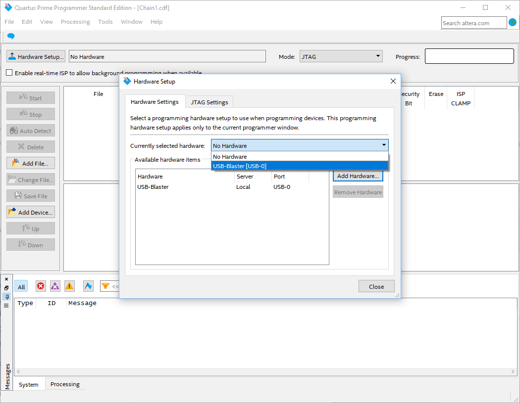
Step 1: Run Quartus Prime Programmer and set up the hardware by clicking “Hardware Setup” as shown below. Select the hardware as “USB-Blaster” or equivalent.
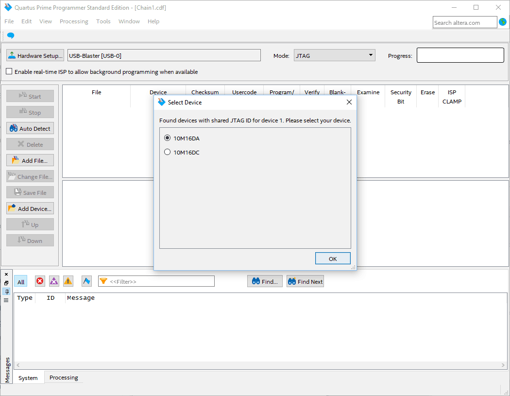
Step 2: Click “Close”. Next, double-click “Auto Detect”, select the device as applicable and click “OK”.
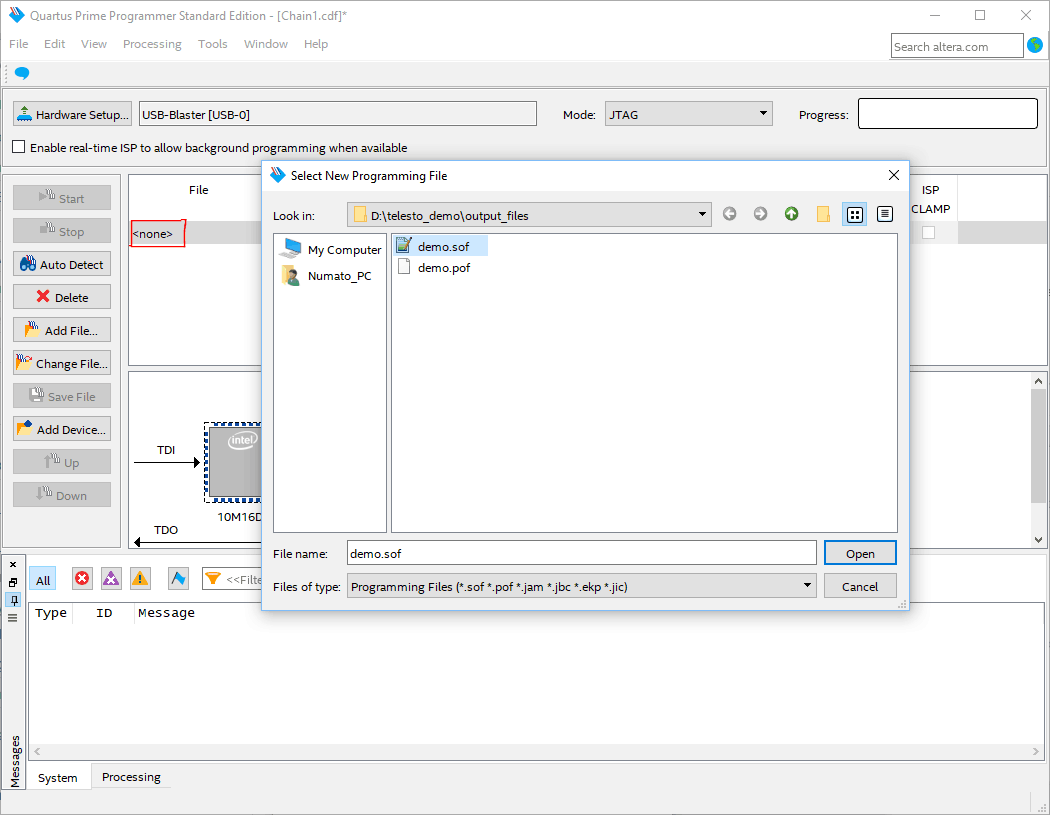
Step 3: Double-click “none” as shown below and select the “.sof/.pof” file to program Telesto with.
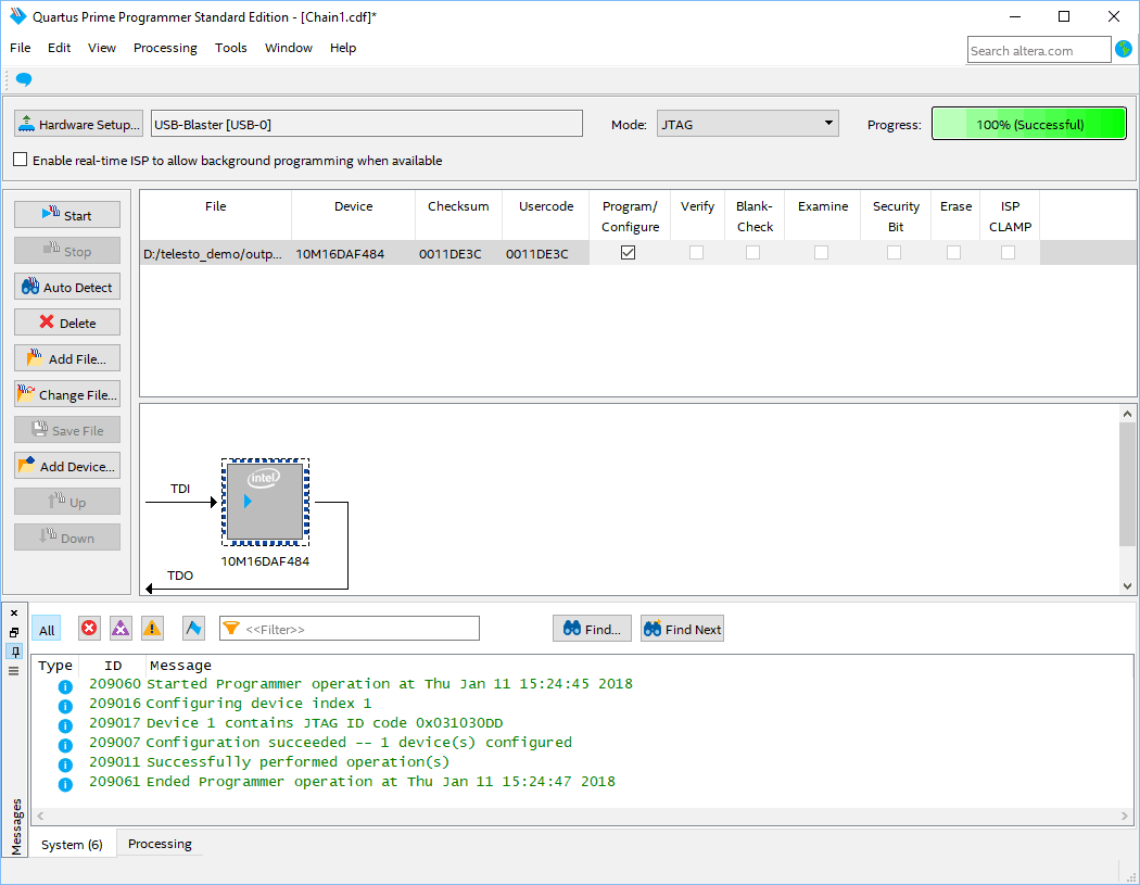
Step 4: Select the “Program/Configure” option and click “Start” to program the FPGA on Telesto.
Programming Telesto using OpenOCD
To program Telesto using OpenOCD using the on-board USB interface on Telesto, please refer to the article “Programming Telesto using OpenOCD” in our Knowledge Base: https://numato.com/kb/programming-telesto-using-openocd/
Technical Specifications
| Parameter * | Value | Unit |
|---|---|---|
| Basic Specifications | ||
| Number of GPIOs | 150 + 8 (Max) | |
| On-board oscillator frequency (ASVMPLV-100.000MHZ-LC-T) | 100 | MHz |
| DDR3 Capacity | 2 | Gb |
| Power supply voltage (External) | 5 - 12 | V |
| FPGA Specifications | ||
| Supply voltage for core and periphery | -0.5 - 1.63 | V |
| Supply voltage for input and output buffers | -0.5 - 3.9 | V |
| Supply voltage for ADC analog block | -0.5 - 3.41 | V |
| Supply voltage for ADC digital block | -0.5 - 1.63 | V |
Mechanical Dimensions