In the previous article, we saw how to build a Linux Kernel and run it on Narvi Spartan 7 FPGA Development Board using Xilinx Platform Cable USB and XSCT console. Though this is the easier method, there are a couple of drawbacks associated with it. You will need a Xilinx Platform Cable USB which is slightly expensive and the images are programmed to SRAM/DDR instead of SPI flash. It is possible to program the onboard SPI flash with the images which would retain contents even after a power cycle and this can be done without buying expensive JTAG cables.
To program the onboard SPI flash, we will need to make a single binary image that will contain the following individual images.
- FPGA bit file for Microblaze
- Linux kernel
- A bootloader
A bootloader is necessary here to copy the Linux kernel from SPI flash to DDR and execute it. The primary requirement for the bootloader is that it should be capable of reading data from the SPI flash and should fit within the BRAM cache size.
First, we need to modify the previous Vivado project.
Step 1:
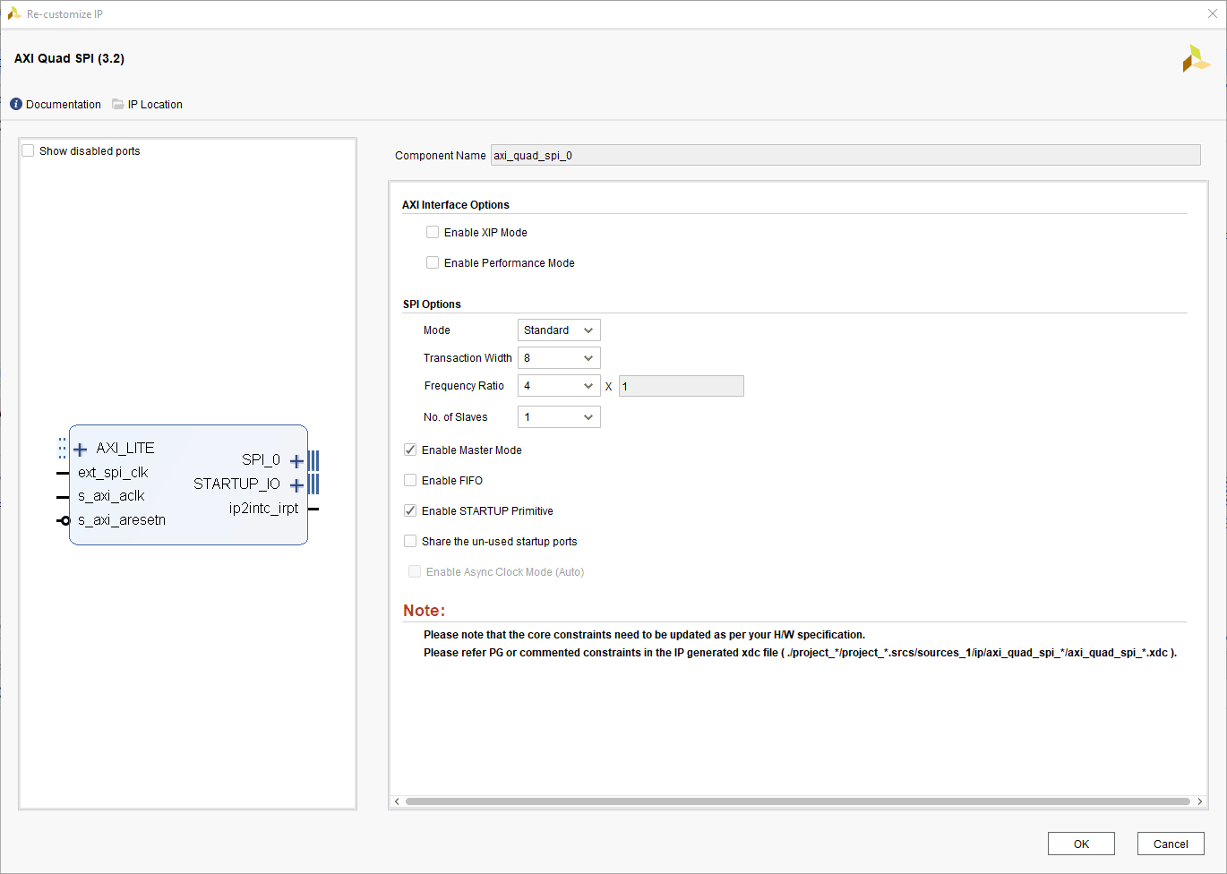
We have already created a block diagram for the previous article, we need to add SPI in the block diagram to be able to use a flash tool, for that open the block diagram in Vivado, click on “add IP” and add “AXI Quad SPI”. Double click on the AXI Quad SPI block and change its settings as shown in the figure. Make sure to check the “Enable STARTUP Primitive” option.
Click on “Run Block Automation” on the top left corner of the window to complete the design. Click “OK” for Vivado to automatically configure the blocks for you. Once Block Automation is complete, Run Connection Automation so Vivado can connect the blocks to make a complete system.
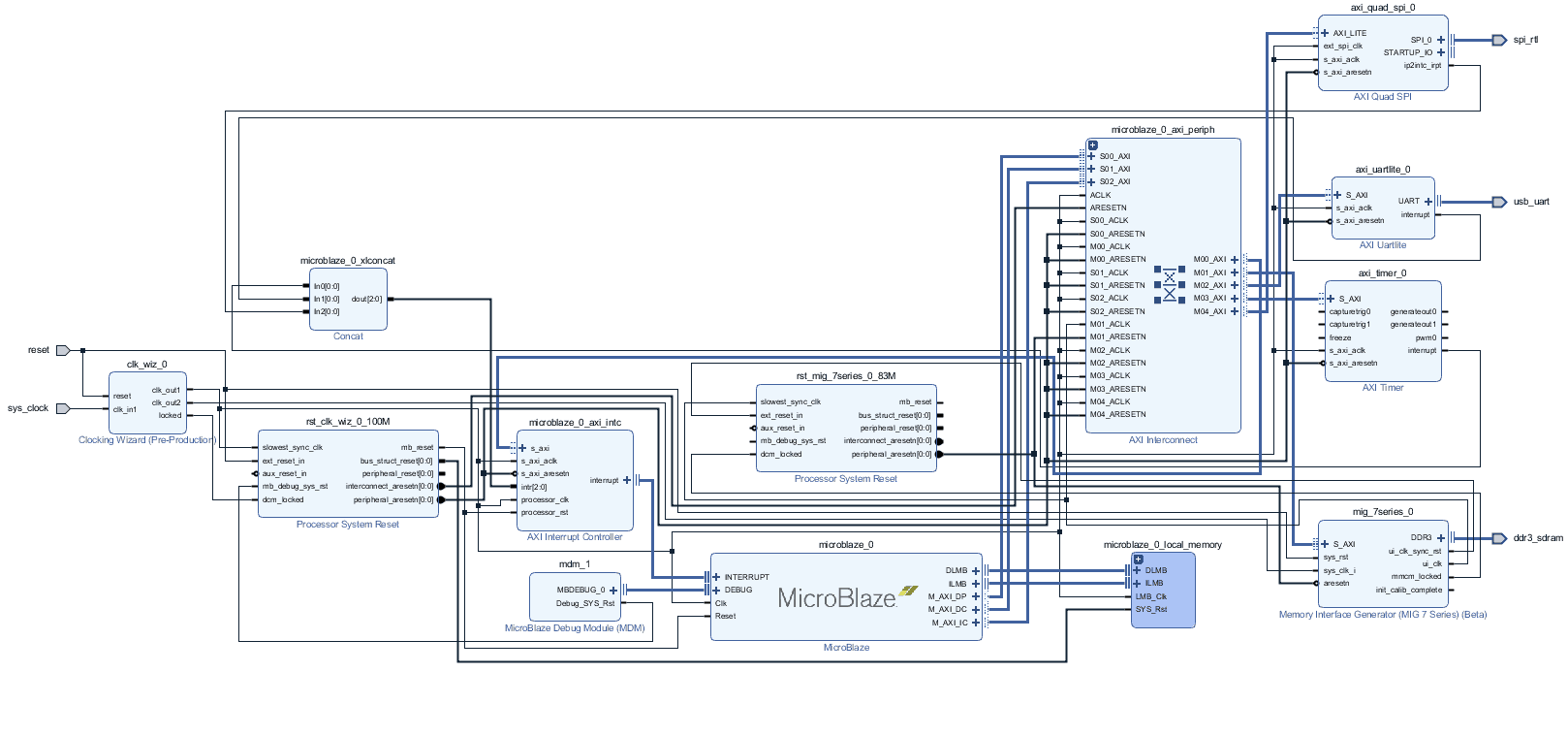
The final diagram should look like this:
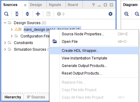
Step 2: Right-click on the block design in the “Sources” window, select “Create HDL Wrapper” from the popup menu. Click “OK” on the window that appears to finish generating the wrapper.
Step 3: Since this project is created using the Narvi BSP file. The Narvi BSP file does not include the QSPI peripheral. Hence here we need to create a Constraints file to add the QSPI pins. Create a Constraints file from the “Sources” window and Copy the below constraints for QSPI to the created Constraints file.
set_property -dict { PACKAGE_PIN "M13" IOSTANDARD LVCMOS33 SLEW FAST} [get_ports { spi_rtl_ss_io }]
set_property -dict { PACKAGE_PIN "K17" IOSTANDARD LVCMOS33 SLEW FAST} [get_ports { spi_rtl_io0_io}]
set_property -dict { PACKAGE_PIN "K18" IOSTANDARD LVCMOS33 SLEW FAST} [get_ports { spi_rtl_io1_io}]
Step 4: Click “Generate Bitstream” under the “Program and Debug” to synthesize and implement the design and to generate the bitstream file for the design. Now that the design is implemented successfully, we need to export the bitstream and other related files to be used with SDK. On the File menu, select Export -> Export Hardware.
Generating Device Tree
Having completed all the steps before, download the device-tree repository from Xilinx’s GitHub account: https://github.com/Xilinx/device-tree-xlnx.git. If you downloaded the zip, extract it in the same location as your SDK workspace. In the case of the author, the directory structure was “D:\Projects\narvi_microblaze\narvi_microblaze.sdk\device-tree-xlnx-master”.
Step 1: In Vivado, select File -> Launch SDK. This opens the Xilinx SDK
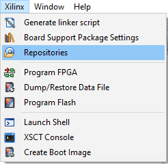
Step 2: In SDK, go to Xilinx Tools/Xilinx -> Repositories.
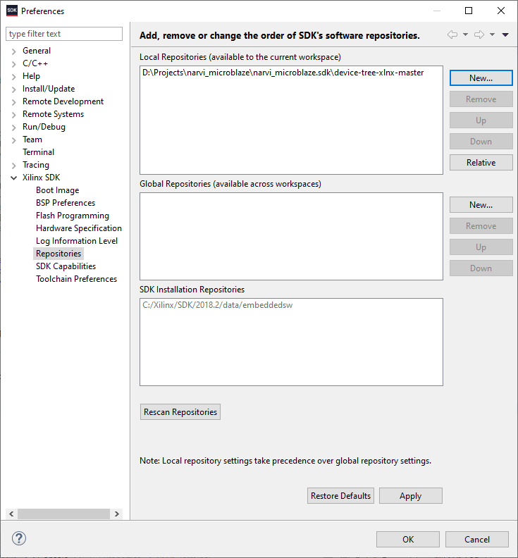
 Step 3: In the dialog window, select “New” and select the device tree folder which you had downloaded and extracted to SDK workspace in the “Local Repositories” section and click “OK”.
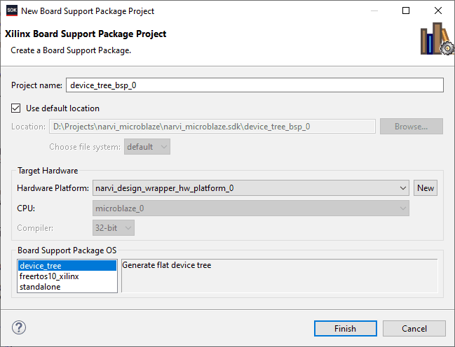
Step 4: Go to File -> New select “Board Support Package”. In the dialog window, select “device_tree” under “Board Support Package OS” and press “Finish” and then “OK” in another dialog that opens.
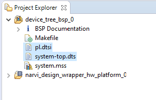
This should generate a ‘system-top.dts’ file along with a ‘.dtsi’ file. We need both of them.
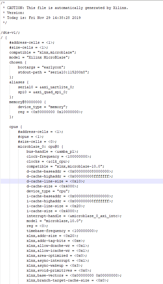
Step 5: We have to merge the ‘.dtsi’ and ‘.dts’ files. Merge these two files using a text editor (like Notepad++ etc) and copy the contents of system-top.dts and paste them in the .dtsi file just after the line ‘model = “Xilinx MicroBlaze”’. Don’t forget to add “/dts-v1/;” at the top of .dtsi file also. The final content should look like this:
Now, save this modified file as “narvi.dts”. Now build a Linux image, for this follow the process same as in the previous article[Link], but use the .dts file that we just created, as it contains the additional needed information about SPI flash.
To build a bootloader, launch SDK from Vivado and create a new application project. Let’s call this project “narvi_linux_bootloader”. When selecting the application template, select “Hello World”. Once the project is created, open the “narvi_linux_bootloader” project in the “Project Explorer” on the left. Double click on the linker script “lscript.ld” and make sure that all sections are mapped to BRAM (should look something like microblaze_0_local_memory_ilmb_bram_if_cntlr_microblaze_0_local_memory_dlmb_bram_if_cntlr). If not, map all sections to BRAM manually and save the linker script. After saving the linker script, build the project and make sure that no errors are reported.
Open helloworld.c in the project and replace the ent+ire code with the code below. Please note, the code below is a bare-bones bootloader designed to be simpler than being robust.
#include <stdio.h>
#include "platform.h"
#include "xparameters.h"
#include "xstatus.h"
#include "xspi.h"
#include "xil_cache.h"

//Set the offset and size of image in SPI flash
#define FLASH_IMAGE_START_ADDRESS 0x500000
#define FLASH_IMAGE_SIZE 0x700000

//Set the address where image will be loaded. This will usually point to
//DDR or SRAM depending on the board architecture. Remember to build
//your application/Linux kernel with this address as base address
#define IMAGE_LOAD_ADDRESS XPAR_MIG_7SERIES_0_BASEADDR

//Define ID of the SPI peripheral that is connected to the SPI flash
#define SPI_DEVICE_ID XPAR_SPI_0_DEVICE_ID

void (*imageEntry)();
XSpi Spi;

u8 spiReadData()
{
    while(!(XSpi_ReadReg(Spi.BaseAddr, XSP_SR_OFFSET) & 0x02));
    return XSpi_ReadReg(Spi.BaseAddr,XSP_DRR_OFFSET);
}

//This function writes one byte to the SPI peripheral
void spiWriteData(u8 data)
{
    while(XSpi_GetStatusReg(&Spi) & 0x08);
    XSpi_WriteReg(Spi.BaseAddr, XSP_DTR_OFFSET, data);
}

int loadAppImage()
{
    XSpi_Config *cfgPtr;
    u8 recBuffer[4];
    u32 i = 0, index = 0, ddrPtr = 0;

    print("Initializing Numato Lab Narvi SPI Linux Image Loader...\n\r");
    print("*** http://numato.com ***\n\r");
    print("\n\r");

    //Lookup SPI peripheral configuration details
    cfgPtr = XSpi_LookupConfig(SPI_DEVICE_ID);
    if (cfgPtr == NULL)
    {
        return XST_DEVICE_NOT_FOUND;
    }

    if(XSpi_CfgInitialize(&Spi, cfgPtr, cfgPtr->BaseAddress) != XST_SUCCESS)
    {
        return XST_FAILURE;
    }

    //Beyond this point we will use only low level APIs in favor of smaller
    //and simpler code.

    //Set up SPI controller. Master, manual slave select. The SPI peripheral
    //is configured with no FIFO
    XSpi_SetControlReg(&Spi, 0x86);

    //Disable interrupts
    XSpi_IntrGlobalDisable(&Spi);

    //Cycle CS to reset the flash to known state
    XSpi_WriteReg(Spi.BaseAddr, XSP_SSR_OFFSET, 0x00);
    XSpi_WriteReg(Spi.BaseAddr, XSP_SSR_OFFSET, 0x01);
    XSpi_WriteReg(Spi.BaseAddr, XSP_SSR_OFFSET, 0x00);

    //Write command 0x0b (fast read) to SPI flash and do a dummy read
    spiWriteData(0x0b);
    spiReadData();

    //Send the address from where the image needs to be loaded.
    //Dummy read after every write as usual
    spiWriteData((FLASH_IMAGE_START_ADDRESS >> 16) & 0xff);
    spiReadData();
    spiWriteData((FLASH_IMAGE_START_ADDRESS >> 8) & 0xff);
    spiReadData();
    spiWriteData((FLASH_IMAGE_START_ADDRESS) & 0xff);
    spiReadData();

    //A dummy write/read as per W25Q128FV datasheet
    spiWriteData(0x00);
    spiReadData();

    print("Loading application image...\n\r");

    for(i=0; i<=FLASH_IMAGE_SIZE; i++)
    {
        //Do a dummy write
        spiWriteData(0x00);

        //Read data back
        recBuffer[index] = spiReadData();
        index++;

        //Write the data to DDR/SRAM four bytes at a time
        if(index >= 4)
        {
            *((u32*)(ddrPtr + IMAGE_LOAD_ADDRESS)) = *((u32*)(&recBuffer));
            ddrPtr += 4;
            index = 0;
        }
    }

    print("Executing application image...\n\r");

    //Invalidate instruction cache to clean up all existing entries
    Xil_ICacheInvalidate();

    //Execute the loaded image
    imageEntry = (void (*)())IMAGE_LOAD_ADDRESS;
    (*imageEntry)();

    //We shouldn't be here
    return 0;
}


int main()
{
    init_platform();
    loadAppImage();
    cleanup_platform();
    return 0;
}
Rebuild the project with newly added code and make sure that no errors are reported. If any errors pop up, please fix them before continuing.
The above code will load the kernel image from SPI flash memory and write to DDR and jump to the kernel entry point. This code assumes that the kernel image is sitting at a specific address in the SPI flash (0x500000 in this case) and has a specific size (0x700000) in this case. 0x700000 is a little bigger than the actual kernel image but that shouldn’t cause any problems. The area starting from 0x000000 to 0x4FFFFF is reserved for FPGA configuration data (enough to hold configuration data for XC7S50 devices whose bitstreams’ size is 2192012 bytes, or 0x21728C bytes in hex). So in essence, we are targeting the following memory map for the SPI flash binary image we are going to create.
- 0x000000 – 0x4FFFFF -> FPGA configuration data
- 0x500000 – 0xBFFFFF -> Kernel image
- 0xC00000 upwards -> User data (not used in our case)
At this point, we have the bit file for FPGA configuration, Linux kernel image and bootloader image we just built. Before we can proceed with packing these images into a single binary file, there is one crucial step we need to do. You may remember the fact that the kernel image we built (simpleimage.narvi) is in ELF format. This is helpful when downloading kernel using XSCT console but the metadata (in addition to executable code) is going to be a problem since our bootloader does not understand ELF format.
One option is to add ELF loader code to the bootloader but it is going to be time-consuming and simply overkill for such a simple implementation like this. Another option would be to strip the metadata and generate a pure executable binary file. This can be easily done with the objcopy tool (objcopy is part of gnu binutils). But the tricky thing here is that you can not use any objcopy (eg: objcopy built for host machine). You will need to use an objcopy that is built for Microblaze.
Fortunately, buildroot already built cross objcopy that runs on the host machine but can work on Microblaze executables. This happened when we built the Linux kernel earlier (buildroot builds all cross tools needed for building the kernel). All that we need to do is to find where these cross-compiled tools are placed by buildroot. With the specific buildroot version we used, the objcopy executable we need was placed in the directory “output/host/usr/microblazeel-buildroot-linux-gnu/bin” under the buildroot root directory.
Switch to output/images directory under buildroot root directory where Linux kernel image is available in ELF format and execute the following command.
../host/usr/microblazeel-buildroot-linux-uclibc/bin/objcopy -O binary simpleImage.narvi narvi_linux.bin
If the command was successful, you will see a new file created with the name narvi_linux.bin. Copy this file over to the Windows machine.
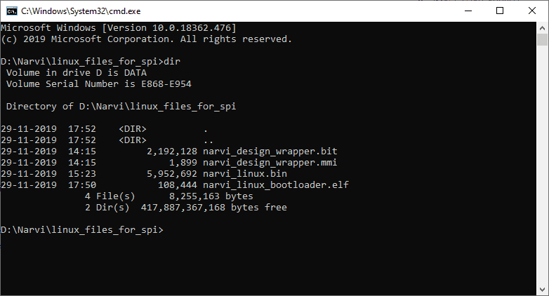
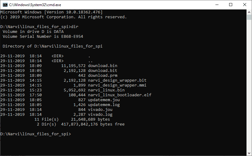
On the Windows machine, place the following files in the same directory.
- The Linux image in binary format narvi_linux.bin (we just created).
- The bit file(.bit) for the Microblaze system and the Memory Map file .mmi) (Both files can be found in your SDK’s Project Explorer under the project named “narvi_design_wrapper_hw_platform_0” or similar. Please see the image below).
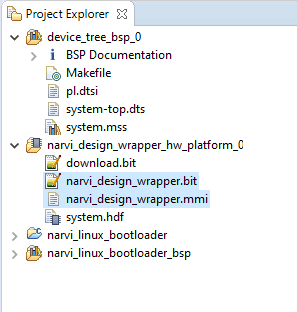
- The bootloader executable (This file can be found in the directory narvi_linux_bootloader\Debug under the SDK bootloader project folder and has .elf extension).
- In the author’s case, the following files are in the ‘linux_files_for_spi’ folder as shown in the image. Your file names may be different depending on the project names etc…
With all the necessary images available now, let us move forward with creating the final binary image. We will do the following steps to create a single binary image.
- Merge the FPGA configuration (.bit file) and the Bootloader executable image (.elf). This is because the contents of the executable need to go into the FPGA BRAM when FPGA initializes after power-up.
- Concatenate the combined FPGA configuration file (generated in the previous step) with the Linux kernel image.
Open the command prompt and ‘cd’ to the directory where the binary files and executable file (in author case the directory is ‘linux_files_for_spi’) are located. Merge the Bootloader executable image with a bit file by running the following commands:
D:\Xilinx\Vivado\2018.2\Vivado\2018.2\bin\vivado.bat -mode tcl
updatemem -force -meminfo "narvi_design_wrapper.mmi" -bit "narvi_design_wrapper.bit" -data "narvi_linux_bootloader.elf" -proc narvi_design_i/microblaze_0 -out "download.bit"
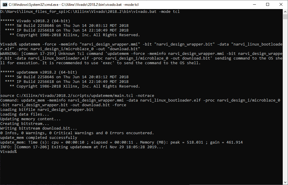
If the command ran successfully, you will see a new file created in the directory with the name “download.bit”. This file now has both the FPGA configuration stream and Bootloader code.
Now we can concatenate the FPGA configuration file we just generated (download.bit) with Linux kernel binary image (narvi_linux.bin) to create a single binary image that can be downloaded to the SPI flash. Run the following commands to generate a single binary image.
write_cfgmem -force -format BIN -size 16 -interface SPIx1 -loadbit "up 0x00 download.bit" -loaddata "up 0x500000 narvi_linux.bin" download.bin
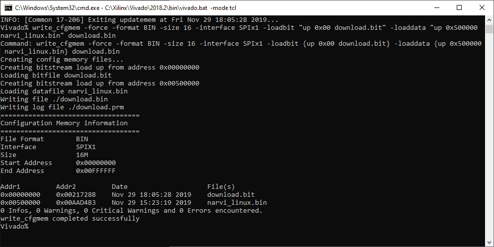
If this command succeeded, you will see a few new files in the directory and one of them would be “download.bin”. This is the final binary image that we need to download to Narvi’s SPI flash. The following image shows all files in my directory after executing all the above-mentioned steps.
The final image is approximately 11.1MB in size and this leaves approximately 4.9MB of available space in the SPI flash for custom user data.
Now Download the latest “Tenagra System Management Software” from the “Downloads” section of the Narvi product page or from the Tenagra product page and use that to download the final binary image “download.bin” to the SPI flash (see image below).
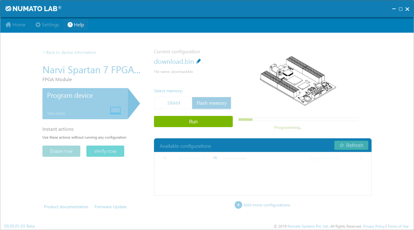
For steps on how to program Narvi using Tenagra, refer the Getting started with Tenagra FPGA System Management Software article.
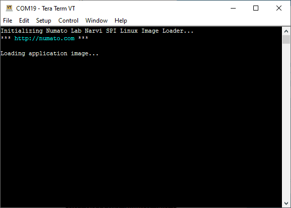
It may take a couple of minutes for the download to complete. While the download is in progress, go ahead and start your favorite serial terminal emulation program (Hyperterminal, PuTTY, TeraTerm, etc.) and open the COM port corresponding to Narvi and set the baud rate to 115200.
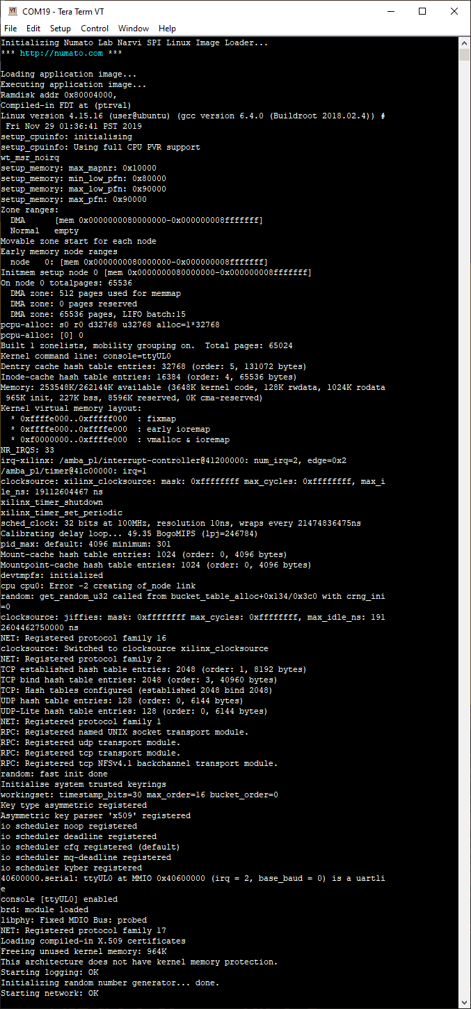
Once the binary image is completed downloading, the tool will reboot the FPGA and let it load the configuration data from the newly downloaded image. If everything went well, the bootloader will start copying a Linux kernel image to DDR and you will see the below message in the serial terminal emulation software.
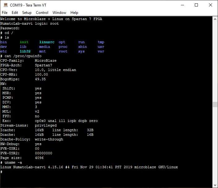
It may take a few seconds for the bootloader to copy the Linux kernel. Once copying is completed, the bootloader will start the kernel and you will see the kernel booting as shown below.
You can log in to Linux as “root” with a password as “Narvi”. The image below shows the root directory structure, cpuinfo and “uname -a” outputs: