So far we learned a few things about Verilog and how to create a module in Verilog and run a simulation. While simulation can tell us a lot of things about the correctness of our module, there is nothing like putting it on a piece of hardware and seeing it working. In this part of the tutorial, we will walk you through the steps for synthesizing the module and implementing it on Mimas A7 FPGA Development Board hardware.
As mentioned in part 3 of this tutorial, the test bench code is used only for simulation. To synthesize our module, we have to remove the test bench code. For those who don’t know, HDL Synthesis is the step where the HDL ( Verilog/VHDL or any other HDL for that matter) is interpreted and an equivalent hardware topology is generated. This hardware topology will be very specific to the target FPGA selected. Synthesis is a very complex process and we don’t need to know the internals to get our simple module up running.
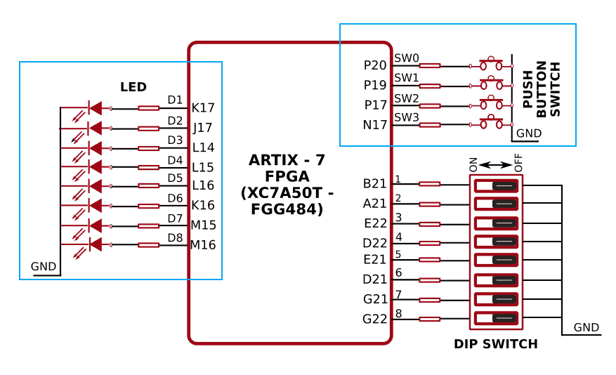
We will use the Mimas A7 FPGA Development Board to implement our module. Mimas A7 board has a Xilinx Artix 7 FPGA, a DDR SDRAM and a few other peripherals on board. The exact FPGA part number used on this board is XC7A50T-1FGG484C. The image below shows the part of the schematics where FPGA IOs for LEDs and Push Button Switches are connected. We will use one Push Button Switch and one LED to implement our logic.
Let’s come back to our module and think about how we can implement the same on the hardware. The module in question is a NOT gate. As we know, the output of a NOT gate is always the negation of the input. We can have many possible hardware configurations to test this module. The easiest would be with a switch and a LED. See the proposed hardware configuration in the picture below.
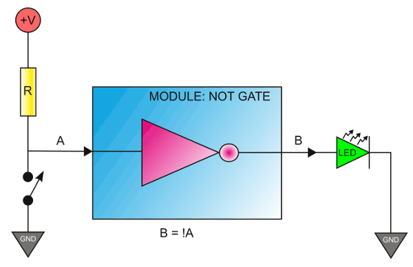
In the above diagram, a switch is connected to an input which is pulled up to VCC using a resistor. The output is connected to a LED. Let’s take a moment to understand how this circuit is going to behave. When the switch is in open position, there will be a positive voltage ie; a logic 1 at the input (A) of the NOT gate. That means the output (B) will be at logic 0. So the LED will be in OFF condition. When the switch is closed, the input of NOT gate will become logic 0 and the output will switch to logic 1 state. And the LED will glow.
Now we know the basic hardware requirements. We need the following in our prospective hardware.
- An input capable IO with a pull-up resistor and a switch attached.
- An output capable IO with an LED attached.
Let’s take a closer look at the Mimas A7 FPGA Development Board. The following image shows the LED and switch we are planning to use on Mimas A7.
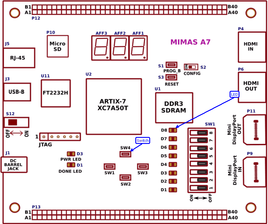
As we see in the image above, Mimas A7 has four general purpose push button switches and eight LEDs for the user’s convenience. We can now take a look at the Mimas A7 schematics and learn a little bit more about where the switches and LEDs are connected. Let’s choose pushbutton switch SW4 and LED D8 for our purpose. Looking through the schematics reveals that SW4 is connected to IO N17 and LED D8 is connected to M16 of the FPGA respectively.
We now have a Verilog module that we want to implement and we have selected a hardware platform and decided what IOs to use for implementation. Let us revisit our module. I’m reposting the module code here.
module myModule(A, B);
   input wire A;
   output wire B;
   assign B = !A;
endmodule
Our module has two ports. Port A, which is the input and Port B, which is the output. An attentive reader would be asking now, how are we going to attach Port A to N17 of the hardware and Port B to M16 of the hardware. We will do this by defining user constraints. User constraints tell the router and the placement logic (which is a part of HDL synthesizer) on which physical pins the module signals are to be connected. We make a list of constraints and place it in a file and include that file in the project. This file is called a User Constraints File. For Xilinx Vivado tools, it is a text file with .xdc extension. Fortunately, the user constraints file for Mimas A7 is already available for download at the product page. This file has definitions for all IOs available on Mimas A7. But we don’t need all of them. So I’ll remove the unused part and post the required file contents here.
Download the XDC file for Mimas A7 from here .
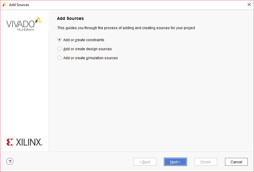
To create the constraints file, follow the steps below:
1. Go to “Add Sources” under the Flow Navigator –> PROJECT MANAGER window, select the “Add or create constraints” and click “Next”.
2. Click on “Create file” and give a name for the XDC and select “File type” as “XDC”. Click “OK” and then “Finish”.
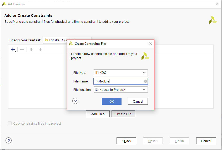
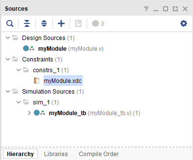
3. The XDC file is now created and is available in the Sources –> Constraints. Double click on it to open.
Now the constraints file for the project is created. In the XDC downloaded from the product, it has constraints for all the peripherals. But we don’t need all of them. So I’ll remove the unused part and paste the required file contents here.
set_property -dict { PACKAGE_PIN "N17"  IOSTANDARD LVCMOS33 SLEW FAST} [get_ports { sw_in[3] }];  # IO_L21P_T3_DQS_14  Sch = SW3
set_property -dict { PACKAGE_PIN "M16"  IOSTANDARD LVCMOS33 SLEW FAST} [get_ports { LED[7] }];    # IO_L24N_T3_RS0_15  Sch = LED7
The content of this file is pretty self-explanatory. On line No.2 it says the net LED (net is equivalent to wire/connection in a physical circuit) is connected to the physical pin M16. Line No. 1 connects the net SW to physical IO N17. Well, this still doesn’t answer how the ports of our module are going to be connected to the switch and LED. Like I have mentioned before, the ports of a module are equivalent to wires going in and out of the module. That, in turn, is equivalent to a net. So we can use the port names as net names in the constraints file. So if we modify above user constraints code for our NOT gate module, it will look something like this.
set_property -dict { PACKAGE_PIN "N17" IOSTANDARD LVCMOS33 SLEW FAST} [get_ports { A }]; # IO_L21P_T3_DQS_14 Sch = SW3
set_property -dict { PACKAGE_PIN "M16" IOSTANDARD LVCMOS33 SLEW FAST} [get_ports { B }]; # IO_L24N_T3_RS0_15 Sch = LED7
Now we have pretty much everything we need to synthesize the design and test it.
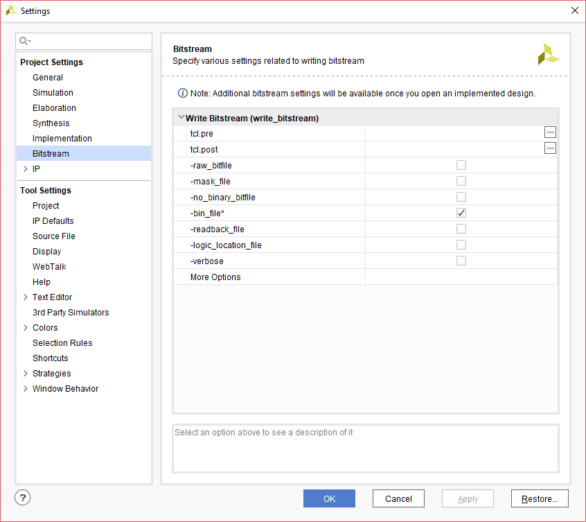
Right click on “Generate Bitstream” in the Flow Navigator panel. Select the “Bitstream Settings” and check the “-bin_file”. Click “Apply” and then “OK”.
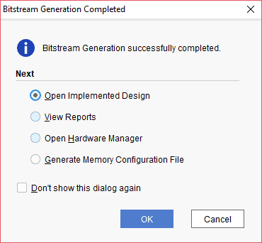
Now click on Generate Bitstream. Click “OK” on the following window that appears. The bitstream generation process may take a while.
Once the bitstream generation is completed, if everything goes well and there are no errors, the following window will be displayed.
If there are any errors or warnings, you can check them in the “messages” window.
Now download myModule.bin (should be in the project directory if everything goes well) to Mimas A7 FPGA development board. Please see the Mimas A7 user manual to find more information about downloading output binary file to Mimas A7. Once downloading is complete, press the switch SW4 and you should see LED8 light up.
Download complete Xilinx Vivado Implementation project for Mimas A7
Back to part 3 Continue to part 5