
Introduction

Mimas A7 is a serious upgrade to our lower-cost Mimas V2 FPGA Development board. Based on Artix 7™ 50T FPGA, Mimas A7 plenty powerful as it is versatile. This FPGA Development Board follows the philosophy of offering a large variety of peripherals on a compact form factor to allow minimal external components to run and evaluate as many designs as possible. Mimas A7 is a great platform for implementing Soft processors such as Microblaze to make it a complete embedded platform. The built-in Gigabit Ethernet offers low latency high bandwidth data transfer to host. The USB 2.0 host interface based on popular FT2232H offers high bandwidth data transfer and board programming without the need for any external programming adapters. Onboard HDMI IN/OUT interfaces along with large DDR3 SDRAM makes Mimas A7 a great platform for video capture, processing, and rendering. The staple peripherals such as switches and seven-segment displays offer great value for learning, prototyping and debugging.
Board Features
- Device: Xilinx Artix 7 FPGA (XC7A50T-1FGG484C)
- DDR3: 2Gb DDR3 (MT41J128M16HA-125 or equivalent)
- Built-in programming interface. No expensive JTAG adapters needed for programming the board
- Onboard 128Mb flash memory for FPGA configuration storage and custom user data storage
- High-Speed USB 2.0 interface for On-board flash programming. FT2232H Channel B is dedicated to SPI Flash /JTAG Programming. Channel A can be used for custom applications.
- 100MHz CMOS oscillator
- Micro SD card slot for memory expansion
- Gigabit Ethernet
- HDMI IN/OUT interfaces
- High-Speed Serial Interface (GTP) available on mini DisplayPort connectors
- 8 LEDs, 4 Push Buttons and 8 way DIP switch for user-defined purposes
- FPGA configuration via JTAG and USB
- Maximum IOs for user-defined purposes
- FPGA – 80 IOs (40 professionally length matched Differential Pairs)
- FT2232H – 8 IOs
Applications
- Product Prototype Development
- Accelerated computing integration
- Development and testing of custom embedded processors
- Signal Processing
- Communication devices development
- Educational tool for Schools and Universities
- Video processing
How to use Mimas Artix 7 FPGA Development Board
The following sections describe in detail how to use this module.
Hardware Accessories Required
For easy and fast installation, you may need the following items along with the Mimas A7 module.
- USB A to USB B cable
- DC Power supply
- A Xilinx Platform Cable USB II compatible JTAG programmer
Connection Diagram
Revision V2.0:
The following connection diagram should be used for reference only. The schematics are available at the end of this document for detailed information.
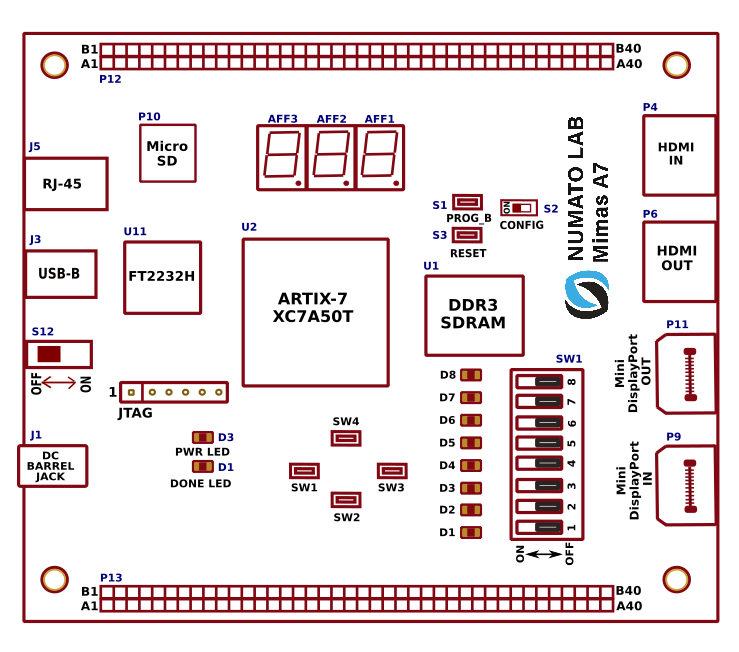
Note: Micro SD slot is available at the bottom side of the board.
Revision V3.0:
The following connection diagram should be used for reference only. The schematics are available at the end of this document for detailed information.
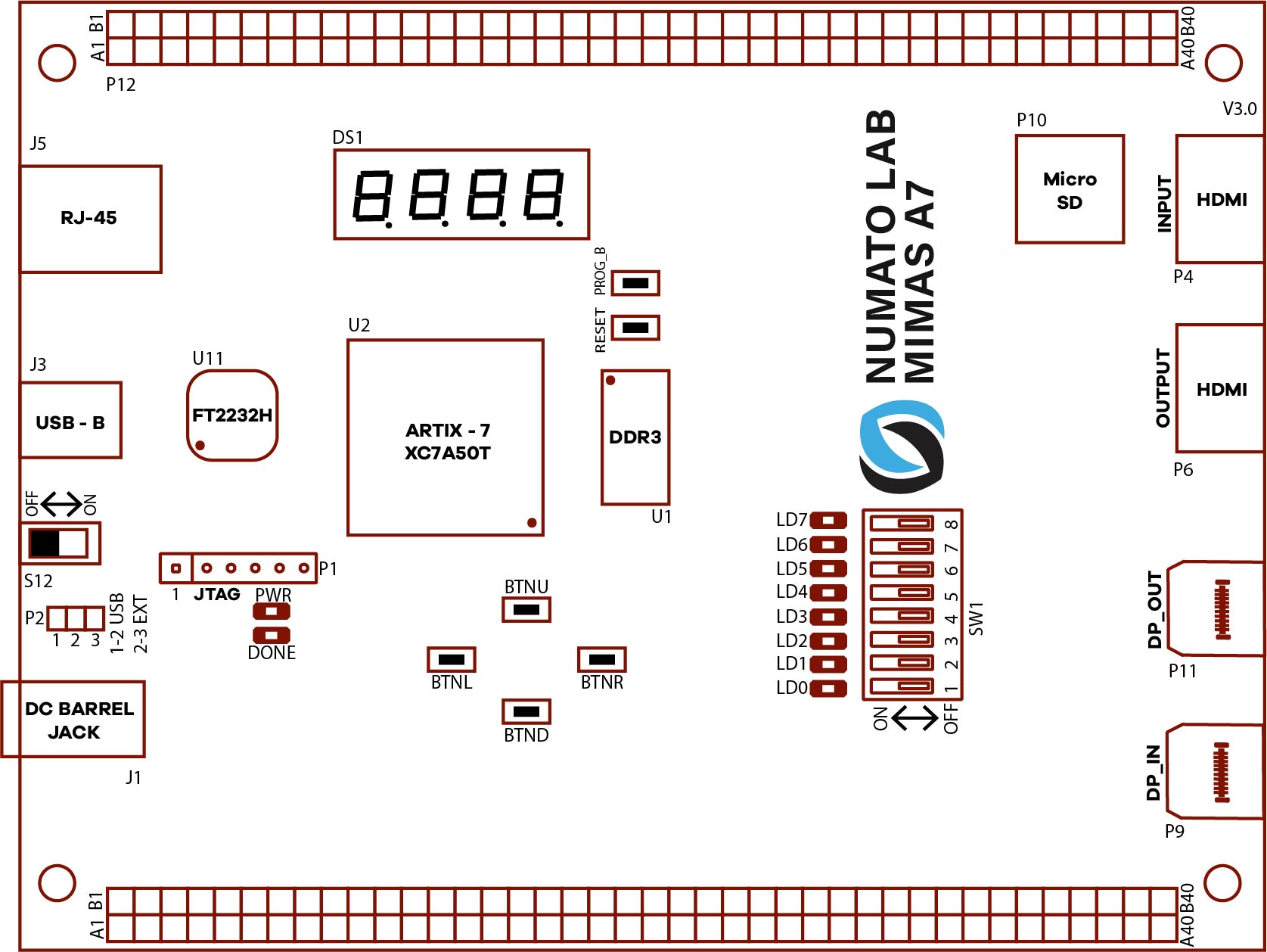
Note: Micro SD slot is available at the bottom side of the board.
USB Interface
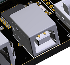 The onboard full-speed USB controller helps a Windows/Linux/Mac computer to communicate with this module. Use a USB A to USB B cable to connect with a PC(the picture on the right shows USB B connector).
DC Power Supply
 The board is configured to use power from DC power supply by connecting it to the External DC Jack. Please refer to the marking on the board for more details. The external power supply should be in the range of +5 to +12V, with sufficient current rating.
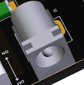
Power Switch
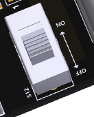 The Power Switch S12 is used to switch on/off the board. Sliding it to ON to supply power to the board from External DC Jack. Sliding it to OFF to power off the board.
For Revision V3.0: There is an option to get powered from the USB also.
The power selection process is discussed in the following section.
Power Select
For Revision V3.0: The Power Select header P2 is used to configure the power source for the board. Connect pins 1 and 2 to use USB power and connect pins 2 and 3 to use the external DC power.
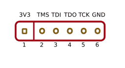
JTAG Connector
JTAG connector allows the FPGA’s JTAG registers to be accessed using a JTAG cable, compatible with Xilinx Platform Cable USB. Use this header, to attach JTAG cable for programming and debugging.
PROG_B and Reset Buttons
PROG_B Button
Mimas A7 features a Push-button S1 normally meant to be used as a “PROG_B” signal for configuration reset. Push-button S1 is connected to FPGA pin N12. For enabling manual configuration reset, push-button S1 is connected to GND. The user can reconfigure the FPGA manually, by pressing this push-button S1.
“PROG_B” is an active-low input pin (pulled up with 4.7K external resistor) to the FPGA and it controls the configuration logic. When the PROG_B pin is de-asserted, resets the FPGA and initializes the new configuration.
Reset Button
Mimas A7 features a Push-button S3 normally meant to be used as a “Reset” signal for designs running on FPGA. Push-button S3 is connected to FPGA pin M2. Push-button S3 is active-high. This pushbutton can also be used for any other input and is not just limited to be used as a Reset signal.
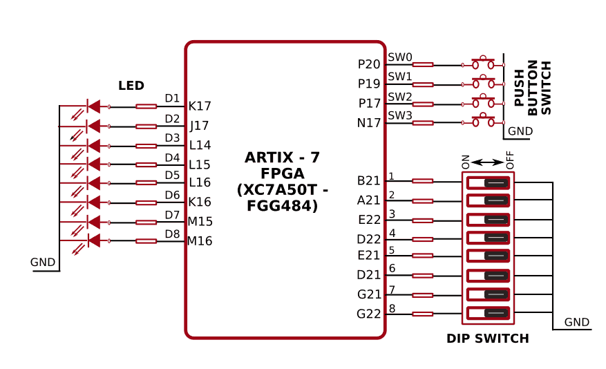
LED, Push Button and Dip Switch
Mimas A7 Development Board has four push-button switches, an eight-position DIP switch and eight LEDs for human interaction. All switches are directly connected to Artix 7 FPGA and can be used in your design with minimal effort.
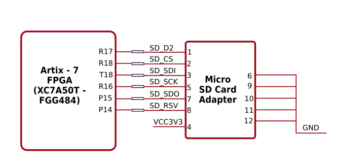
Micro SD
The Mimas A7 board features an onboard Micro SD adapter. You can add the data logging, media storage, and other file storage by installing Micro SD Card and appropriate IP. The connection between FPGA and Micro SD Card is shown below
7-Segment LED Display
Revision V2.0:
This version of the board features three 7-segment LED display multiplexed for low pin count operation. Each module can be separately turned on and off with the three switching transistors.
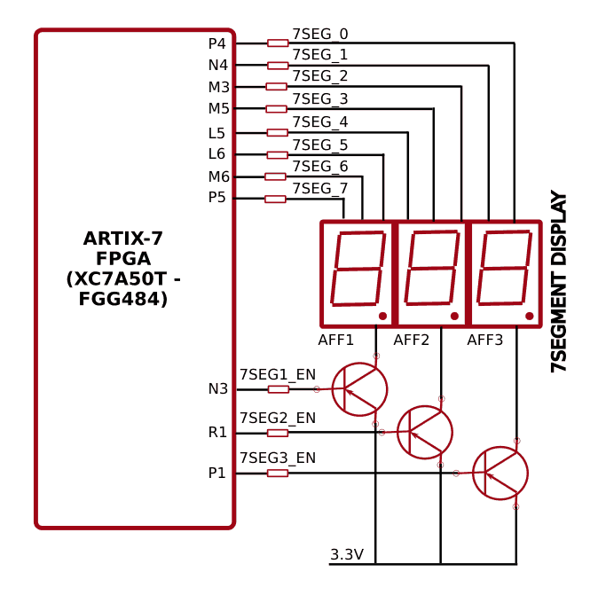
Note: All signals (a, b, c, d, e, f, g, dot, enable 1, enable 2, enable 3) used for controlling 7-Segment display are active-low signals. So, for example, for displaying “8” in display-2, users need to drive Enable 2 to 0 as well as drive signals a, b, c, d, e, f to 0. All other signals need to be driven to 1.
Revision V3.0:
This version of the board features four 7-segment LED displays. Each module can be separately turned on and off with the four switching transistors.
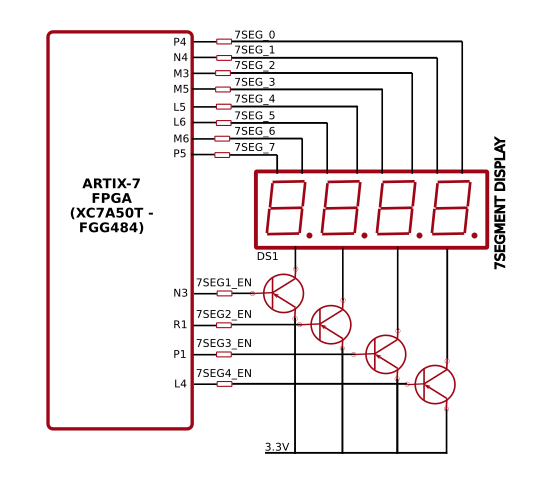
Note: All signals (a, b, c, d, e, f, g, dot, enable 1, enable 2, enable 3, enable 4) used for controlling 7-Segment display are active-low signals. So, for example, for displaying “8” in display-2, users need to drive Enable 2 to 0 as well as drive signals a, b, c, d, e, f to 0. All other signals need to be driven to 1.
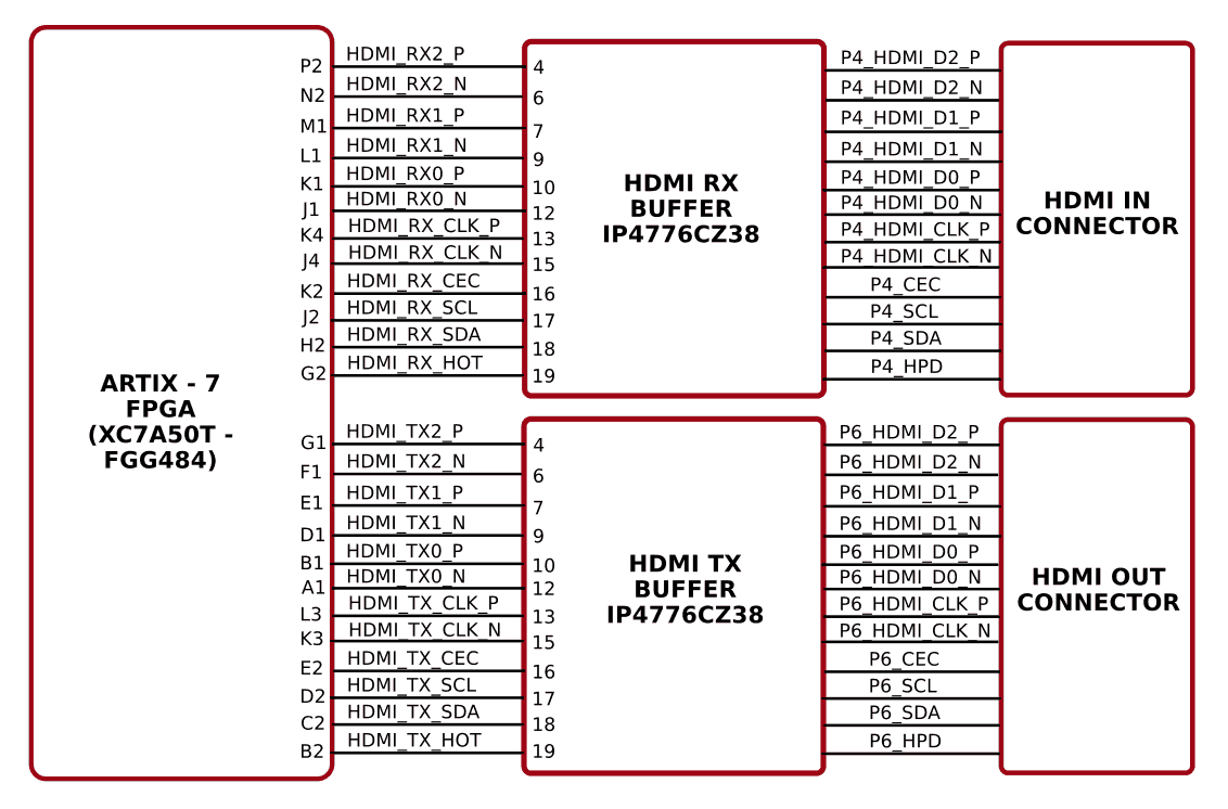
DVI-D/HDMI
Onboard HDMI IN/OUT interfaces along with large DDR3 SDRAM makes Mimas A7 a great platform for video capture, processing, and rendering. The HDMI IN/OUT interfaces are buffered using HDMI buffer IP4776CZ38 for better signal strength and signal integrity.
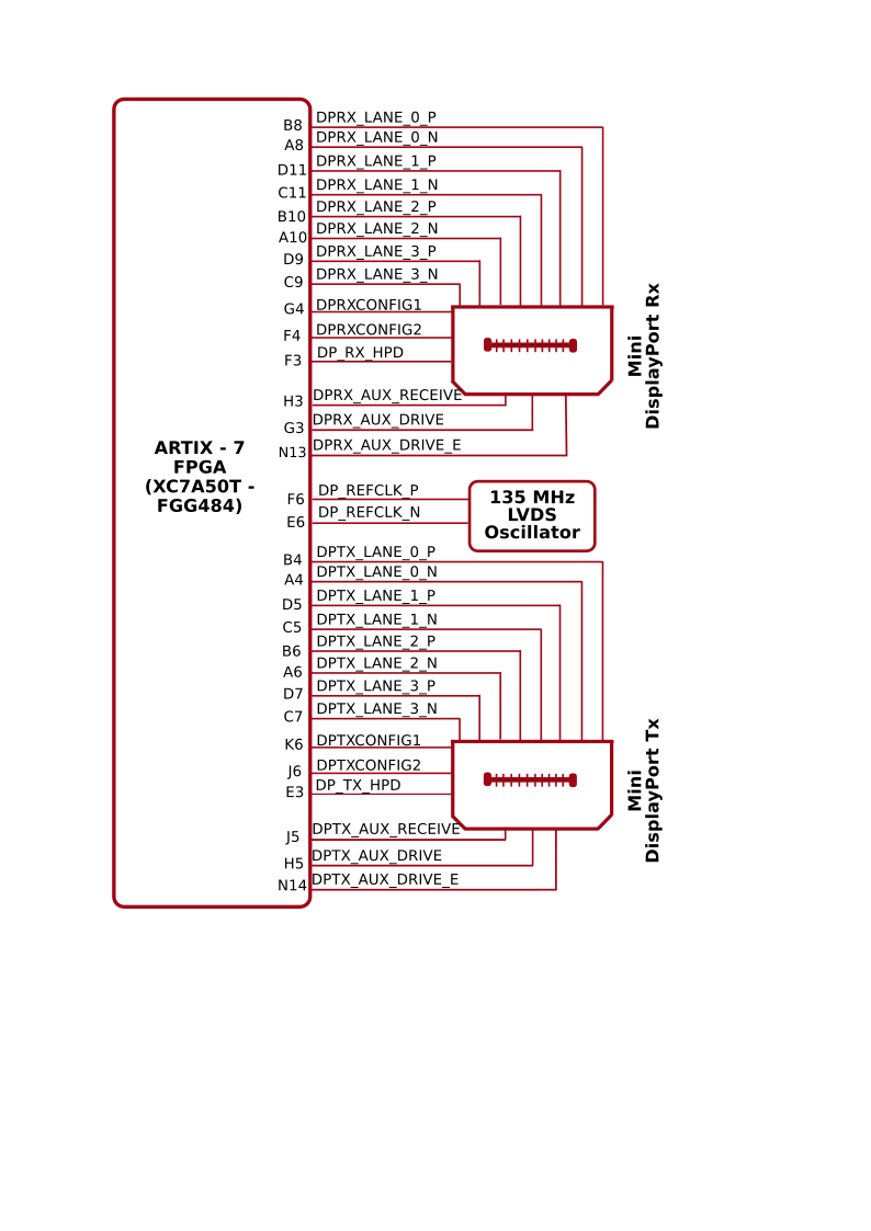
Mini Display Port
Mimas A7 includes onboard mini DisplayPort (miniDP or mDP) IN/OUT connectors and it is a miniaturized version of DisplayPort digital display technology. The mini DisplayPort is having four lanes along with auxiliary channel and a hot plug detect the signal. High-Speed Serial Interface (GTP) available on mini DisplayPort connectors.
Revision V2.0:

Revision V3.0:
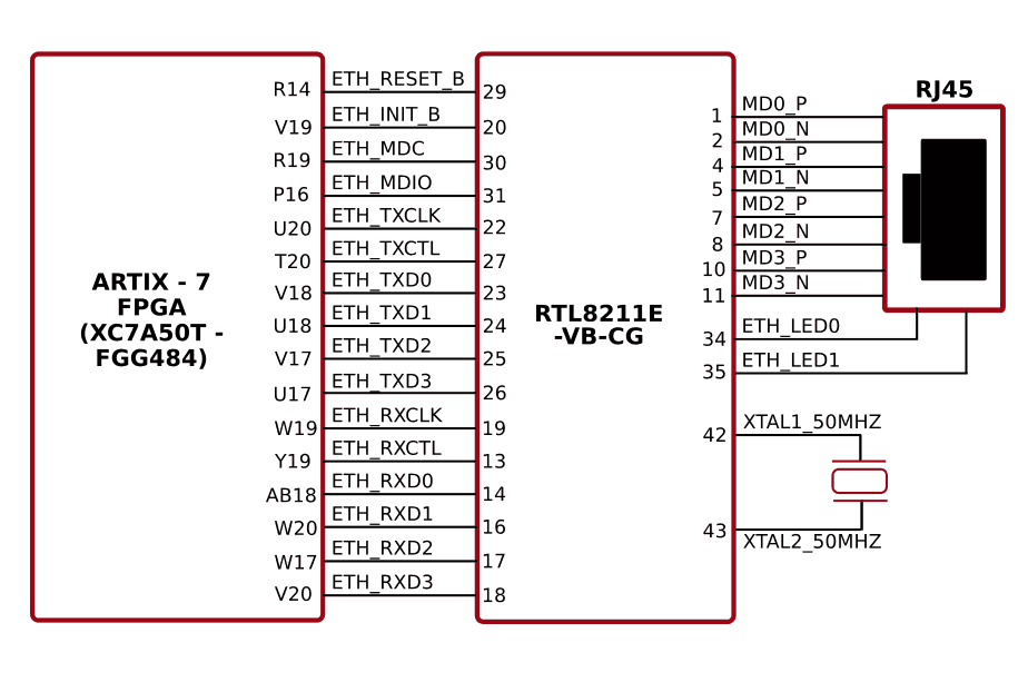
Gigabit Ethernet
Mimas A7 Development Board features RTL8211E, a highly integrated Ethernet transceiver from Realtek that comply with 10BASE-T, 100BASE-TX, and 1000Base-T IEEE 802.3 standards. It supports communication with the Ethernet MAC layer via standard RGMII interface. RTL8211E-VB implements auto-negotiation to automatically determine the best possible speed and mode of operation. It contains a high-performance 10/100/1000T transceiver and the RGMII interface supports 1000Mbps (1Gbps) operation.
JTAG/SPI Configuration on FT2232H Channel B
Channel B of FT2232H can be connected to the SPI bus that connects the SPI Flash chip to the FPGA or to the JTAG pins of the FPGA. When FT2232H channel B is connected to FPGA JTAG, the JTAG signals can be accessed directly through FT2232H. This is the default configuration set when Mimas A7 is shipped.
Please see the tables below for information about selecting SPI or JTAG for FT2232H channel B.
Solder Jumpers P3
| Jumper Configuration for SPI | Jumper Configuration for JTAG |
|---|---|
| 1 - 2 | 1 - 3 |
| 5 - 6 | 4 - 6 |
Solder Jumpers P8
| Jumper Configuration for SPI | Jumper Configuration for JTAG |
|---|---|
| 1 - 2 | 1 - 3 |
| 5 - 6 | 4 - 6 |
By default, Mimas A7 ships with the solder jumpers in JTAG configuration. During normal usage, users should not change these jumpers from their factory default configuration.
GPIOs
This device is equipped with a maximum of 80 user IO pins that can be used for various custom applications. All user IOs are length matched and can be used as differential pairs.
Header P12
| Pin No. On The Header | GPIO Pin Name | Artix-7 (FGG484) Pin No. | Pin No. On The Header | GPIO Pin Name | Artix-7 (FGG484) Pin No. |
|---|---|---|---|---|---|
| A1 | VIN | B1 | VIN | ||
| A2 | VIN | B2 | VIN | ||
| A3 | GND | B3 | GND | ||
| A4 | GPIO_1_P | J20 | B4 | GPIO_1_N | J21 |
| A5 | GPIO_2_P | K21 | B5 | GPIO_2_N | K22 |
| A6 | GPIO_3_P | H20 | B6 | GPIO_3_N | G20 |
| A7 | GPIO_4_P | J19 | B7 | GPIO_4_N | H19 |
| A8 | GND | B8 | GND | ||
| A9 | VCC_VADJ | B9 | VCC_VADJ | ||
| A10 | GPIO_5_P | J22 | B10 | GPIO_5_N | H22 |
| A11 | GPIO_6_P | K18 | B11 | GPIO_6_N | K19 |
| A12 | GPIO_7_P | L19 | B12 | GPIO_7_N | L20 |
| A13 | GPIO_8_P | M21 | B13 | GPIO_8_N | L21 |
| A14 | GND | B14 | GND | ||
| A15 | VCC_VADJ | B15 | VCC_VADJ | ||
| A16 | GPIO_9_P | N22 | B16 | GPIO_9_N | M22 |
| A17 | GPIO_10_P | N20 | B17 | GPIO_10_N | M20 |
| A18 | GPIO_11_P | M18 | B18 | GPIO_11_N | L18 |
| A19 | GPIO_12_P | N18 | B19 | GPIO_12_N | N19 |
| A20 | GND | B20 | GND | ||
| A21 | VCC_VADJ | B21 | VCC_VADJ | ||
| A22 | GPIO_13_P | H17 | B22 | GPIO_13_N | H18 |
| A23 | GPIO_14_P | G17 | B23 | GPIO_14_N | G18 |
| A24 | GND | B24 | GND | ||
| A25 | GPIO_15_P | G15 | B25 | GPIO_15_N | G16 |
| A26 | GPIO_16_P | J15 | B26 | GPIO_16_N | H15 |
| A27 | GND | B27 | GND | ||
| A28 | GPIO_17_P | K13 | B28 | GPIO_17_N | K14 |
| A29 | GPIO_18_P | M13 | B29 | GPIO_18_N | L13 |
| A30 | GND | B30 | GND | ||
| A31 | GPIO_19_P | J14 | B31 | GPIO_19_N | H14 |
| A32 | GPIO_20_P | H13 | B32 | GPIO_20_N | G13 |
| A33 | GND | B33 | GND | ||
| A34 | Vp | L10 | B34 | Vn | M9 |
| A35 | VBAT | E12 | B35 | RESET | M2 |
| A36 | GND | B36 | GND | ||
| A37 | SPI_CS_N | T19 | B37 | SPI_DQ3 | R21 |
| A38 | SPI_DQ1 | R22 | B38 | SPI_SCK | L12 |
| A39 | SPI_DQ2 | P21 | B39 | SPI_DQ0 | P22 |
| A40 | GND | B40 | GND |
Header P13
| Pin No. On The Header | GPIO Pin Name | Artix-7 (FGG484) Pin No. | Pin No. On The Header | GPIO Pin Name | Artix-7 (FGG484) Pin No. |
|---|---|---|---|---|---|
| A1 | VIN | B1 | VIN | ||
| A2 | VIN | B2 | VIN | ||
| A3 | GND | B3 | GND | ||
| A4 | GPIO_21_P | F19 | B4 | GPIO_21_N | F20 |
| A5 | GPIO_22_P | E19 | B5 | GPIO_22_N | D19 |
| A6 | GPIO_23_P | D20 | B6 | GPIO_23_N | C20 |
| A7 | GPIO_24_P | C22 | B7 | GPIO_24_N | B22 |
| A8 | GND | B8 | GND | ||
| A9 | VCC_VADJ | B9 | VCC_VADJ | ||
| A10 | GPIO_25_P | F18 | B10 | GPIO_25_N | E18 |
| A11 | GPIO_26_P | C18 | B11 | GPIO_26_N | C19 |
| A12 | GPIO_27_P | D17 | B12 | GPIO_27_N | C17 |
| A13 | GPIO_28_P | B20 | B13 | GPIO_28_N | A20 |
| A14 | GND | B14 | GND | ||
| A15 | VCC_VADJ | B15 | VCC_VADJ | ||
| A16 | GPIO_29_P | B17 | B16 | GPIO_29_N | B18 |
| A17 | GPIO_30_P | A18 | B17 | GPIO_30_N | A19 |
| A18 | GPIO_31_P | E16 | B18 | GPIO_31_N | D16 |
| A19 | GPIO_32_P | B15 | B19 | GPIO_32_N | B16 |
| A20 | GND | B20 | GND | ||
| A21 | VCC_VADJ | B21 | VCC_VADJ | ||
| A22 | GPIO_33_P | A15 | B22 | GPIO_33_N | A16 |
| A23 | GPIO_34_P | C14 | B23 | GPIO_34_N | C15 |
| A24 | GND | B24 | GND | ||
| A25 | GPIO_35_P | A13 | B25 | GPIO_35_N | A14 |
| A26 | GPIO_36_P | C13 | B26 | GPIO_36_N | B13 |
| A27 | GND | B27 | GND | ||
| A28 | GPIO_37_P | D14 | B28 | GPIO_37_N | D15 |
| A29 | GPIO_38_P | E13 | B29 | GPIO_38_N | E14 |
| A30 | GND | B30 | GND | ||
| A31 | GPIO_39_P | F13 | B31 | GPIO_39_N | F14 |
| A32 | GPIO_40_P | F16 | B32 | GPIO_40_N | E17 |
| A33 | GND | B33 | GND | ||
| A34 | TCK | V12 | B34 | TDO | U13 |
| A35 | TDI | R13 | B35 | TMS | T13 |
| A36 | GND | B36 | GND | ||
| A37 | INIT_B | U12 | B37 | PROGRAM_B | N12 |
| A38 | DONE | G11 | B38 | M0 | U11 |
| A39 | M1 | U10 | B39 | M2 | U9 |
| A40 | GND | B40 | GND |
FT2232H - Artix-7 (FGG484) FPGA Connection Details
| FTDI Pin No. | Pin Function (245 FIFO) | Artix-7 (FGG484) Pin No. |
|---|---|---|
| 16 | FTDI-D0 | Y22 |
| 17 | FTDI-D1 | Y21 |
| 18 | FTDI-D2 | AB22 |
| 19 | FTDI-D3 | AA21 |
| 21 | FTDI-D4 | AB21 |
| 22 | FTDI-D5 | AA20 |
| 23 | FTDI-D6 | AB20 |
| 24 | FTDI-D7 | AA18 |
| 26 | FTDI-RXF# | W21 |
| 27 | FTDI-TXE# | V22 |
| 28 | FTDI-RD# | AA19 |
| 29 | FTDI-WR# | W22 |
| 30 | FTDI-SIWUA | U21 |
| 32 | FTDI-CLKOUT | Y18 |
| 33 | FTDI-OE# | T21 |
Driver Installation
Windows
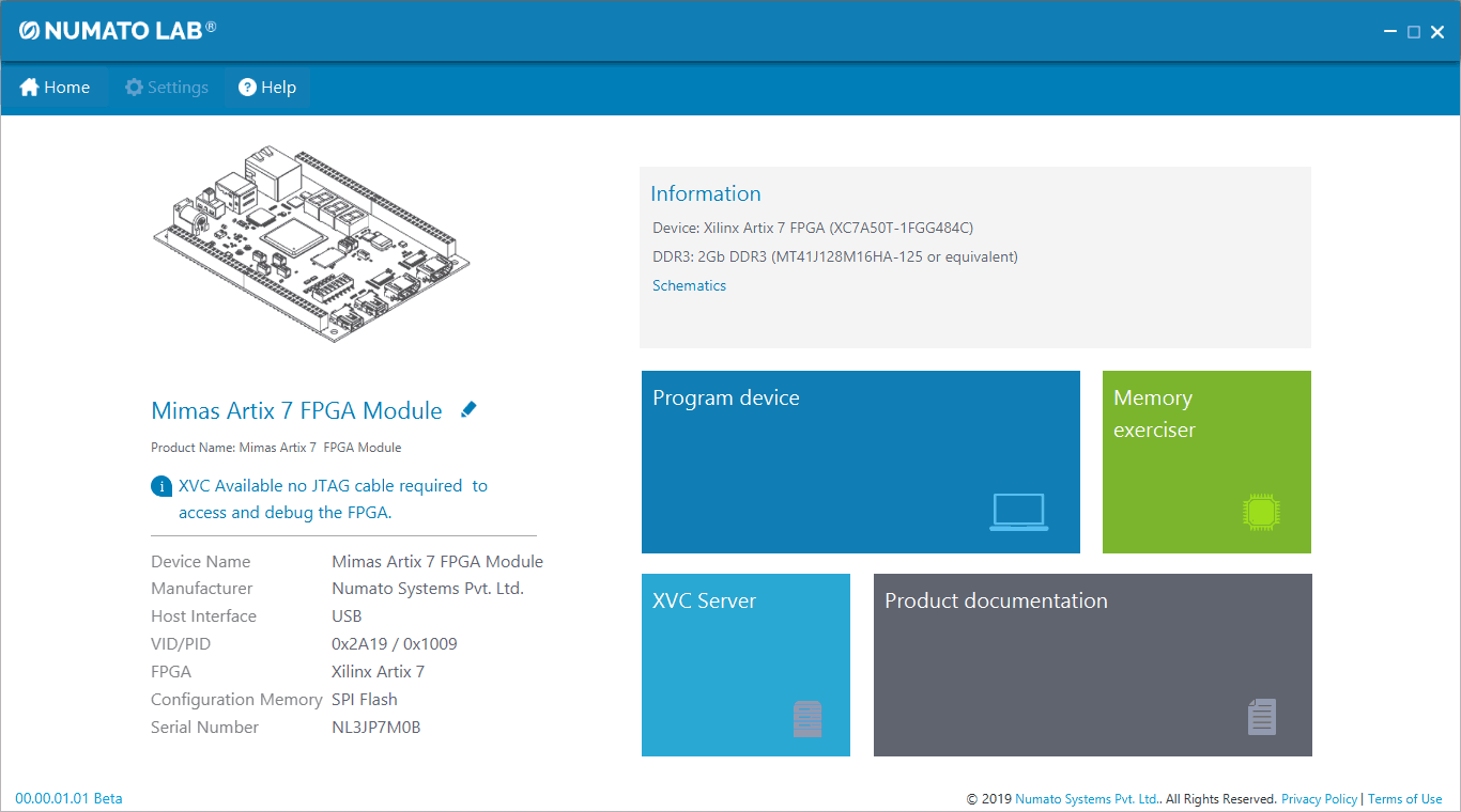
This product requires a driver to be installed for proper functioning when used with Windows. The Numato Lab Mimas A7 driver can be downloaded from here. When the driver installation is complete, the module should appear in Mimas A7 Flash Config Tool as Mimas Artix-7 FPGA Development Board.
Linux
The Linux ships with the drivers required for Mimas A7. It should be enough to run the following two commands in the terminal:
>> sudo modprobe ftdi_sio
>> echo "2a19 1009" | sudo tee /sys/bus/usb-serial/drivers/ftdi_sio/new_id
Generating Bitstream for Mimas A7
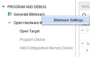
The bitstream can be generated for Mimas A7 in Vivado by following the steps below:
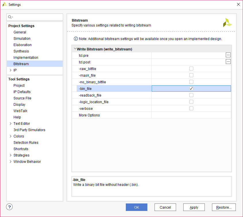
Step 1: It is recommended to generate a .bin bitstream file along with .bit bitstream file. Click “Bitstream Settings”.
Step 2: In the window that pops up, select the “-bin_file*” option and click OK.
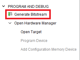
Step 3: Finally click “Generate Bitstream”.
Powering UP Mimas A7
Mimas A7 can be powered directly from an external supply. It is practically very difficult to estimate the power consumption of the board, as it depends heavily on your design and the clock used. XILINX provides tools to estimate power consumption. Mimas A7 requires three different voltages, a 3.3V, a 1.8V supply, and a 1.2V supply. On-board regulators drive these voltages from the External power supply.
Configuring Mimas A7
The Mimas Artix -7 Development Board can be configured by two methods,
- Using the Tenagra application.
- Using the Xilinx Platform Cable USB II or any compatible JTAG hardware
Configuring Mimas A7 using Tenagra
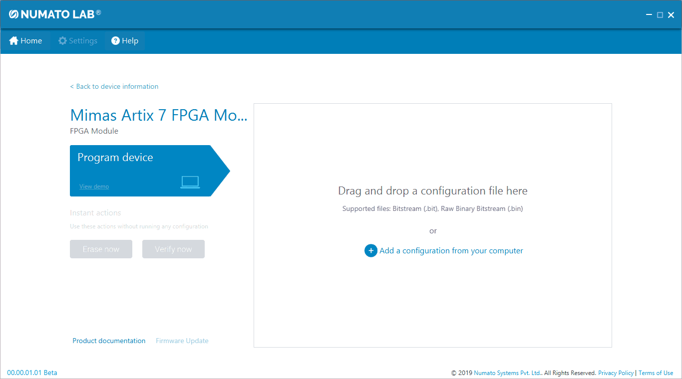
Mimas A7 FPGA Board can be configured using Numato Lab’s Tenagra application. Using Tenagra we can program bitstream files to the SRAM and SPI Flash. Mimas A7 has an onboard FTDI FT2232H device which facilitates easy reprogramming of onboard SPI flash through the USB interface. The FTDI receives bitstream from the host application and programs it into the SPI Flash. The Numato Lab’s Tenagra application can be downloaded from here. The steps below show how to program the Mimas A7 FPGA Board in Tenagra.
Step 1: Open the Tenagra application. Click “Refresh” if Mimas A7 FPGA Board is not detected automatically. And select the Mimas A7 FPGA Board in the list of boards section.

Step 2: Click on the “Program Device” tab to program the board.
Step 3: Then to add Configuration Files click on “Add a configuration from your computer”.
Programming to SRAM
Select the bitstream file (.bit or .bin) which you wish to program on the board and select the “SRAM” tab and then click on the “Run” tab. This will program the board with the selected bitstream file.
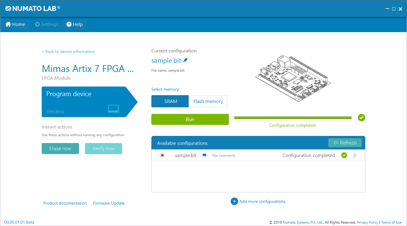
Programming to SPI Flash
Select the bitstream file (only .bin) which you wish to program on the board and select the “Flash Memory” tab and then click on the “Run” tab. This will Configure, Erase, Program and Verify the board with the selected binary file.

Configuring Mimas A7 using JTAG
Mimas A7 – Artix-7 Development Board features an onboard JTAG connector which facilitates easy reprogramming of SRAM and on-board SPI flash through JTAG programmer like “XILINX Platform-cable usb”. Programming Mimas A7 using JTAG requires “XILINX Vivado Hardware Manager” software which is bundled with XILINX Vivado Design Suite. To program the SPI flash we need a “.mcs/.bin” file needs to be generated from the “.bit” file. Steps for generating “.mcs/.bin” file are as below. Programming FPGA SRAM does not require a “.mcs/.bin” file to be generated.
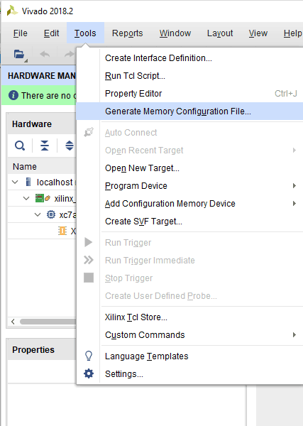
Generating Memory Configuration file for Mimas A7 using Vivado
The screenshots showed in the following steps are captured from the Vivado Design Suite 2018.2.
Step 1: Open Xilinx Vivado Hardware Manager. Connect the board, click “Generate Memory Configuration File….” from the “Tools” menu. “Write Memory Configuration File” pop up window will open.
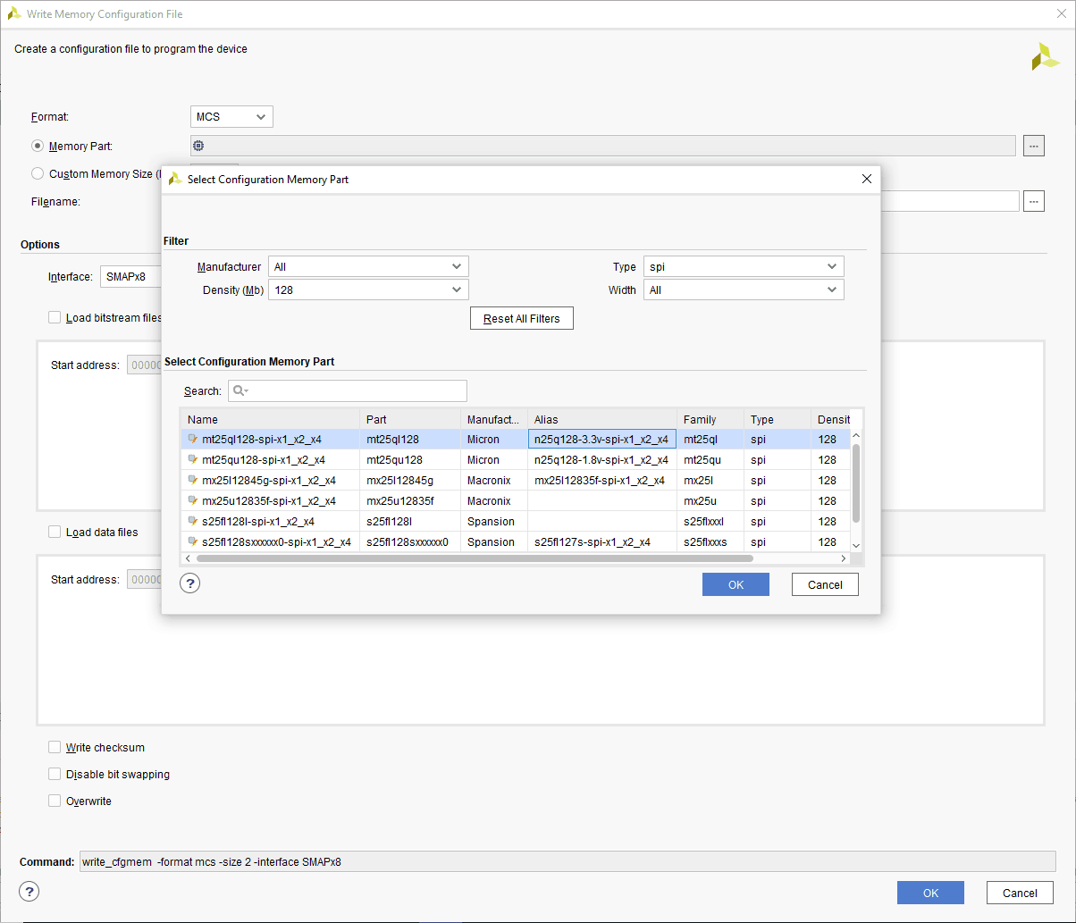
Step 2: Select the ‘Format’ and Configuration Memory Part as shown below. Choose the format as MCS/BIN/HEX depends on your requirements. Now, click “OK”.
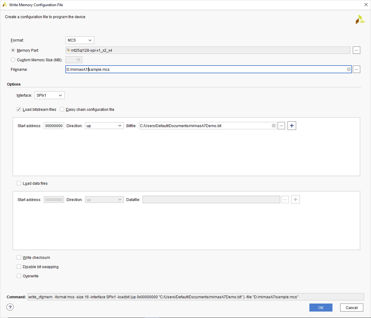
Step 3: Browse the path and type the file name as “sample.mcs” to save the memory configuration file (The format of the file may change depends on your “Format”). Select the “Load bitstream files” under the ”Options” tab and browse the “.bit” file we already generated then click “OK” to generate the memory configuration file.
Programming QSPI Flash using Vivado
A .bin or .mcs file is required for programming Mimas A7’s onboard QSPI flash.
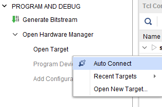
Step 1: Open the Vivado project and open the target by clicking on the “Open Target” in “Open Hardware Manager” in the “Program and Debug” section of the Flow Navigator window. Select “Auto Connect”.
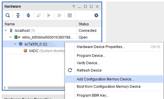
Step 2: If the device is detected successfully, then select “Add Configuration Memory Device” by right click on the target device “xc7a50t_0” as shown below.
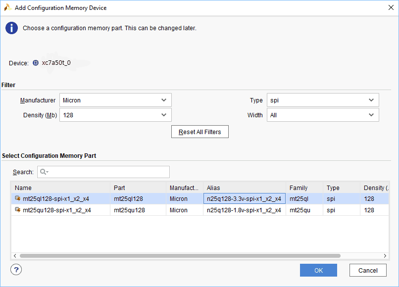
Step 3: Select the memory device “mt25ql128-spi-x1_x2_x4 (which is equivalent to n25q128-3.3v-spi-x1_x2_x4)”, then click OK.
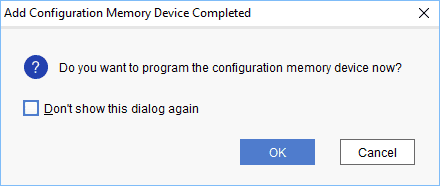
Step 4: After completion of Step 3 the following dialog box will open. Click OK.
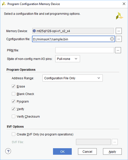
Step 5: Browse to the working .bin file or the .mcs file (whichever applicable) and click OK to program as shown below. If programming is successful, a confirmation message will be displayed.
Programming FPGA using Vivado
Mimas A7 – Artix-7 FPGA Development Board features an onboard JTAG connector that facilitates easy reprogramming of SRAM and onboard SPI flash through JTAG programmer like “Xilinx Platform cable USB”. The following steps illustrate how to program FPGA on Mimas A7 using JTAG.
Step1: By using JTAG cable, connect Xilinx platform cable USB to Mimas A7 and power it up.
Step2: Open the Vivado project and open the target by clicking on the “Open Target” in “Open Hardware Manager” in the “Program and Debug” section of the Flow Navigator window. Select “Auto Connect”.
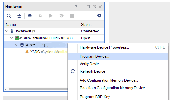
Step3: If the device is detected successfully, then select “Program Device” by right click on the target device “xc7a50t_0” as shown below.
Step4: In the dialog window which opens up, Vivado automatically chooses the correct bitstream file if the design was synthesized, implemented and bitstream generated successfully. If needed, browse to the bitstream which needs to be programmed to FPGA. Finally, click “Program”.
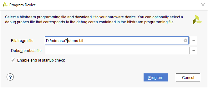
As soon as “Program” is clicked, a red-colored LED (D1) on Mimas A7 should light up, indicating that the programming process is going on. This LED will turn off when the configuration is complete.
Technical Specifications
| Parameter * | Value | Unit |
|---|---|---|
| Basic Specifications | ||
| Number of GPIOs | 80 | |
| On-board oscillator frequency (ASEM1-100.000MHZ-LC-T) | 100 | MHz |
| DDR3 SDRAM (MT41J128M16HA - 125 or Equivalent) | 2 | Gb |
| Quad SPI Flash Memory (N25Q128A13ESE40E) | 128 | Mb |
| Power supply voltage (USB or External) | 5 - 12 | V |
| Number of LEDs | 8 | |
| Number of Push Buttons | 4 | |
| Number of Dip Switches | 8 | |
| FPGA Specifications | ||
| Internal supply voltage relative to GND | -0.5 to 1.1 | V |
| Auxiliary supply voltage relative to GND | -0.5 to 2.0 | V |
| Output drivers supply voltage relative to GND | -0.5 to 3.6 | V |
* All parameters considered nominal. Numato Systems Pvt Ltd reserves the right to modify products without notice.
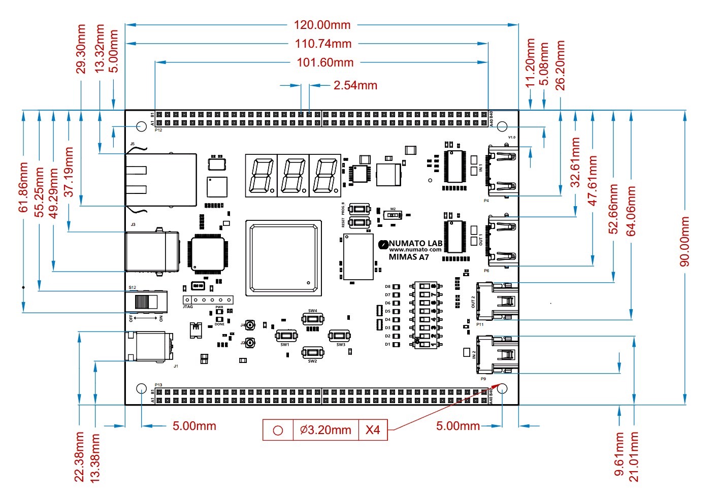
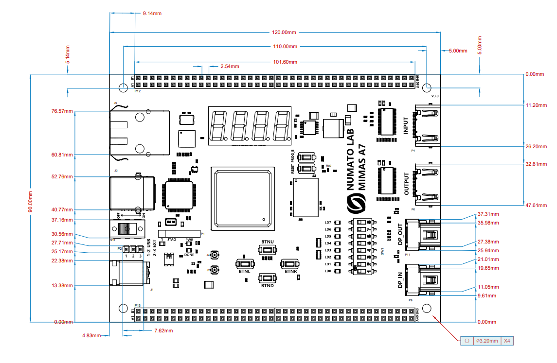
Physical Dimensions
Revision V2.0:
Revision V3.0:
Vivado XDC Constraints
Revision V2.0: Download XDC Constraints for Vivado
Revision V3.0: Download XDC Constraints for Vivado