Introduction:
HDMI (High-Definition Multimedia Interface) is an audio/video interface for transmitting uncompressed video data and compressed or uncompressed digital audio data from an HDMI-compatible source device, such as a display controller, a compatible computer monitor, video projector, digital television, or digital audio device. HDMI transfers the audio or video data between devices with high quality. The pixel data is serially transferred at a speed of ten times the pixel clock frequency using TMDS (Transition Minimized Differential Signalling) to minimize the transitions between 1s and 0s. HDMI is a digital replacement for analog video standards. This article actually demonstrates DVI-D output using Mimas A7 FPGA Development Board. The principles of both HDMI and DVI-D are the same. So all HDMI monitors are capable of receiving the DVI-D signals transported over HDMI cable.
Prerequisites:
- Hardware:
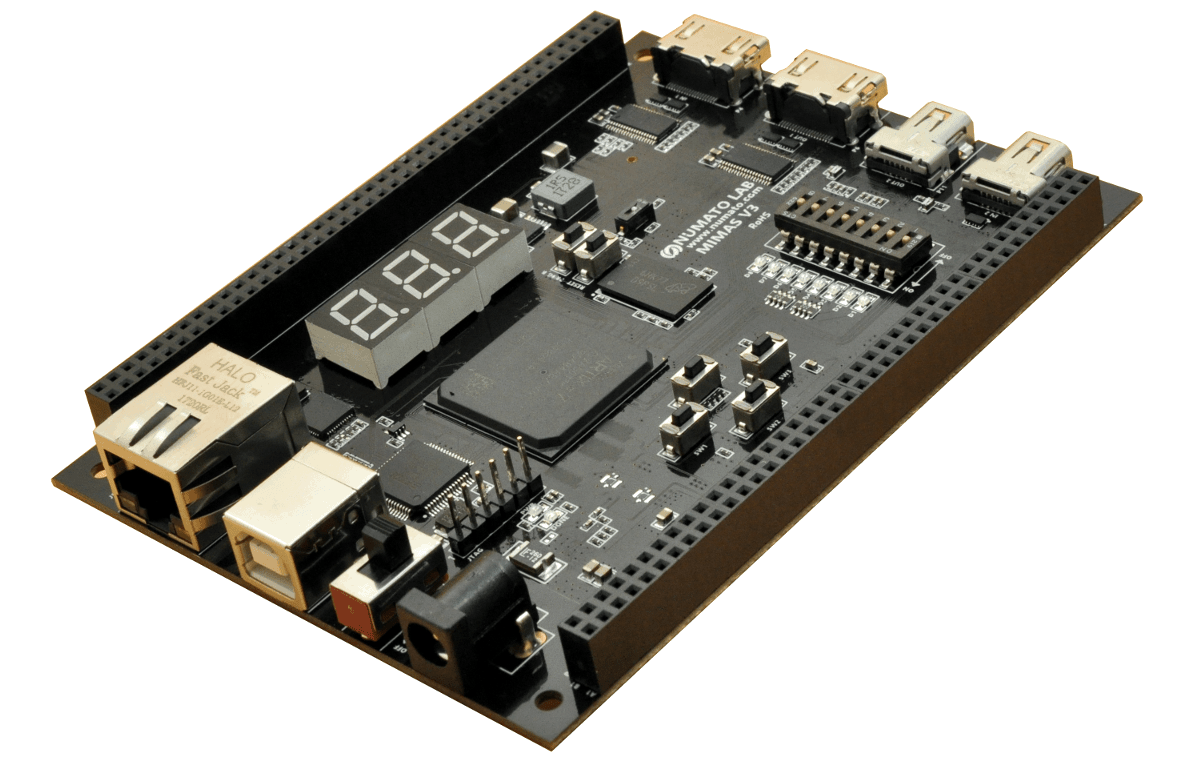
- Mimas A7 FPGA Devolopment Board
- Xilinx Platform Cable USB II JTAG (Optional)
- HDMI cable and a compatible monitor
- USB 2.0 B-type cable
- 5V-12V DC Power Supply (Optional)
- Software:
- Xilinx Vivado Design Suite (version 2023.2.1 or any version)
Let’s get started
The following steps will walk you through the process of creating the HDMI output project on Mimas A7 using Xilinx Vivado Design Suite.
Step 1:
Download and install Vivado Board Support Package files for Mimas A7 from here. Follow the README.md file on how to install Vivado Board Support Package files for Numato Lab boards.
Step 2:
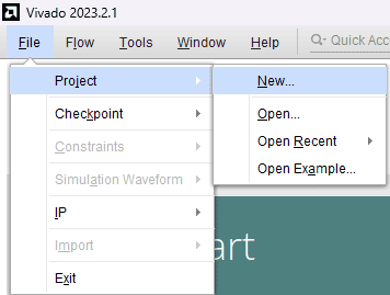
Open Vivado Design Suite, go to File->New->Project. The “New Project” window will open and click “Next” in the New Project wizard.
Step 3:
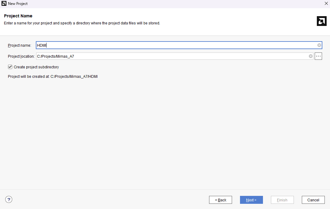
In “Project Name” window, enter a name for the project and save it at a suitable location. Select the option “Create project subdirectory”. Click “Next” to continue.
Step 4:
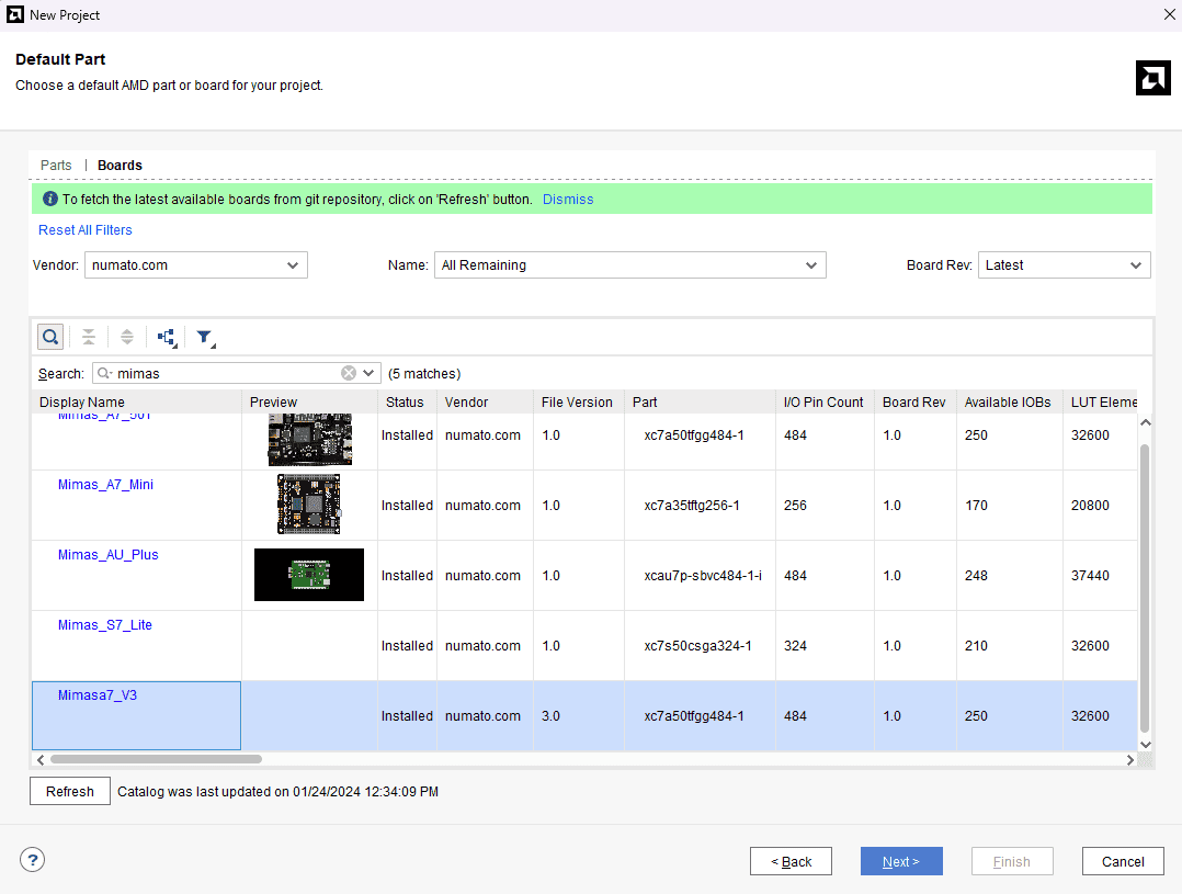
In the “Project Type” window, select “RTL project” and select “Do not specify source at this time” box that appears. Click “Next” to proceed. In the next wizard, select “Mimas_A7_50T” from “Boards” option. If Mimas_A7_50T is not listed, make sure board support files are installed correctly.
Click “Next” and “Finish” to complete creating a new project. A new project will be created by Vivado with the selected settings.
Step 5:
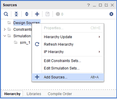
In the “Sources” tab, right-click on the “Design Sources” and select “Add Sources”. It will open a new “Add Sources” window.
Step 6:
Download and extract the RTL source files from here. Add the RTL source file by selecting “Add Files”
The HDMI interface has three pairs of differential data signals each one pair is for each color i.e Red, Blue and Green and one pair of differential clock signals:
data_p[2:0] & data_n[2:0]: These differential signals in HDMI interface carry the audio/video data to display on the screen.
clk_p & clk_n: These are the pixel clock differential signal of HDMI interface.
First, VGA signals are generated inside “vga” module. Then the VGA signals are encoded to 10-bits per channel and the data is then serialized to 10x of pixel clock rate. Finally, the three channels along with pixel clock are driven out using TMDS differential drivers.
The source file has top module (dvid_test) in which two sub modules are instantiated (dvid & vga). This module also include the Clocking IP core to generate required clocks for VGA and DVI-D.
clocking : This module generates required clocks for VGA and DVI-D. The 100MHz clock from the on board oscillator is an input and this input clock drive the other three clocks from it.In this module clk_in (100MHz) is the input clock and the clk_dvi (125MHz), clk_dvin (125MHz), clk_vga (25MHz) are the output clocks for VGA and DVI-D. clk_dvin is 180 degrees out of phase to clk_dvi. These clocks are used for serialization using ODDR2. This module is also having Active High reset signal.
vga: VGA signals are generated in this module with 640×480@60Hz resolution at 25 MHz pixel clock frequency.
dvid: The signals generated from the clocking module and vga module are given as input to dvid module and the DVI-D TMDS signals are generated as the output. It uses TMDS_encoder module to generate TMDS signals. TMDS uses 8b/10b encoding in which the 8-bit color data (red, green & blue) generated in VGA module and is converted to 10 bits. Then this data is serialized using ODDR2 (Double Data Rate primitive). The 10-bit TMDS data is generated at 25 MHz. ODDR2 uses 5 times the frequency of pixel clock (i.e. 125MHz) to serialize the 10-bit encoded data. Note that ODDR2 serializes 2-bits in 1 clock cycle of 125MHz clock. This serialized data is converted into differential signals in the top module (dvid_test) using OBUFDS drivers.
Step 7:
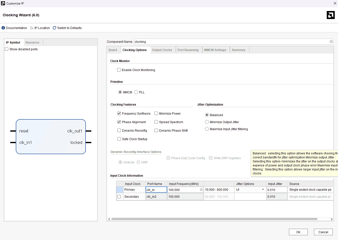
In the “Flow Navigator” panel, click “IP Catalog” under the “PROJECT MANAGER” section. In the IP Catalog, search for “Clocking Wizard” IP and double click on it. The “Customize IP” window will open.

Step 8:
In “Clocking Options” tab, give Component Name as “clocking” and primary clock port name as “clk_in”.
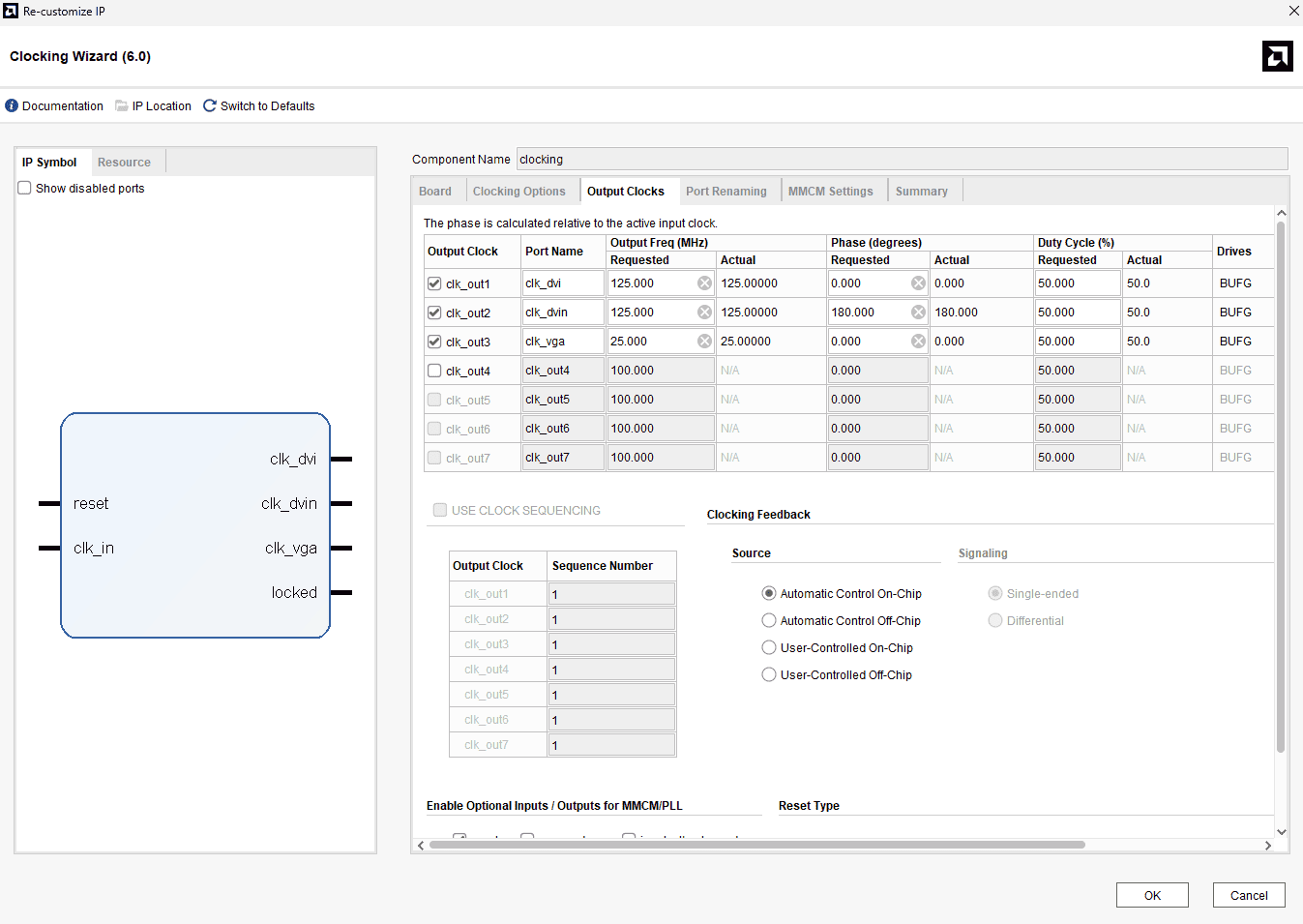
In “Output Clocks” tab, enable 3 output clocks and provide their name, frequency as well as phase as shown below. Click “OK”.
Step 9:
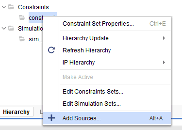
Go to “Add Sources” under the Flow Navigator -> PROJECT MANAGER window, select the “Add or create constraints” and click “Next”. Click on “Create file” and give a name for the XDC and select “File type” as “XDC”. Click “OK” and “Finish”.
Step 10:
Copy the following constraints to the newly created constraints file:
set_property CFGBVS VCCO [current_design]
set_property CONFIG_VOLTAGE 3.3 [current_design]
##Clock Signal
set_property -dict { PACKAGE_PIN "H4"    IOSTANDARD LVCMOS33 } [get_ports { clk_in }];
set_property -dict { PACKAGE_PIN "M2"    IOSTANDARD LVCMOS33 } [get_ports { reset }];
###HDMI out
set_property -dict { PACKAGE_PIN A1    IOSTANDARD TMDS_33  } [get_ports { data_n[0] }];
set_property -dict { PACKAGE_PIN B1    IOSTANDARD TMDS_33  } [get_ports { data_p[0] }];
set_property -dict { PACKAGE_PIN D1    IOSTANDARD TMDS_33  } [get_ports { data_n[1] }];
set_property -dict { PACKAGE_PIN E1    IOSTANDARD TMDS_33  } [get_ports { data_p[1] }];
set_property -dict { PACKAGE_PIN F1    IOSTANDARD TMDS_33  } [get_ports { data_n[2] }];
set_property -dict { PACKAGE_PIN G1    IOSTANDARD TMDS_33  } [get_ports { data_p[2] }];
set_property -dict { PACKAGE_PIN K3    IOSTANDARD TMDS_33  } [get_ports { clk_n}];
set_property -dict { PACKAGE_PIN L3    IOSTANDARD TMDS_33  } [get_ports { clk_p}];
Step 11:
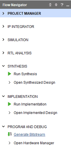
In Flow Navigator panel, click “Generate Bitstream” to synthesize, implement and to generate bitstream.
Step 12:
Set up the hardware for testing the design. Connect the HDMI cable to monitor from the Mimas A7 FPGA Board’s HDMI_OUT port and power up the Mimas A7 board.
Step 13:
To program the MimasA7 with the generated bitstream, follow the steps mentioned below:
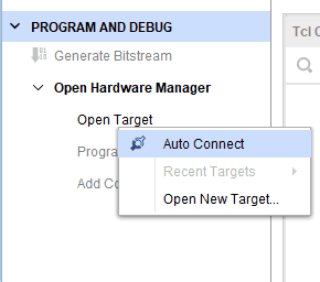
- Once the Bitstream is generated successfully, expand the “Open Hardware Manager” under “PROGRAM AND DEBUG” section of Flow Navigator panel.
- Then click “Open Target->Auto Connect”.
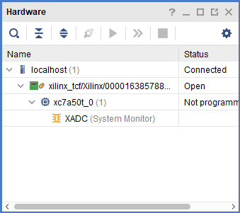
You can now see that the board is detected.
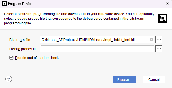
Now, right click on the device “xc7a50t_0 (1)”and click “Program Device”.
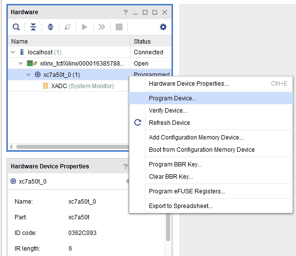
Select the mimas a7 HDMI out bitstream and click “Program”.
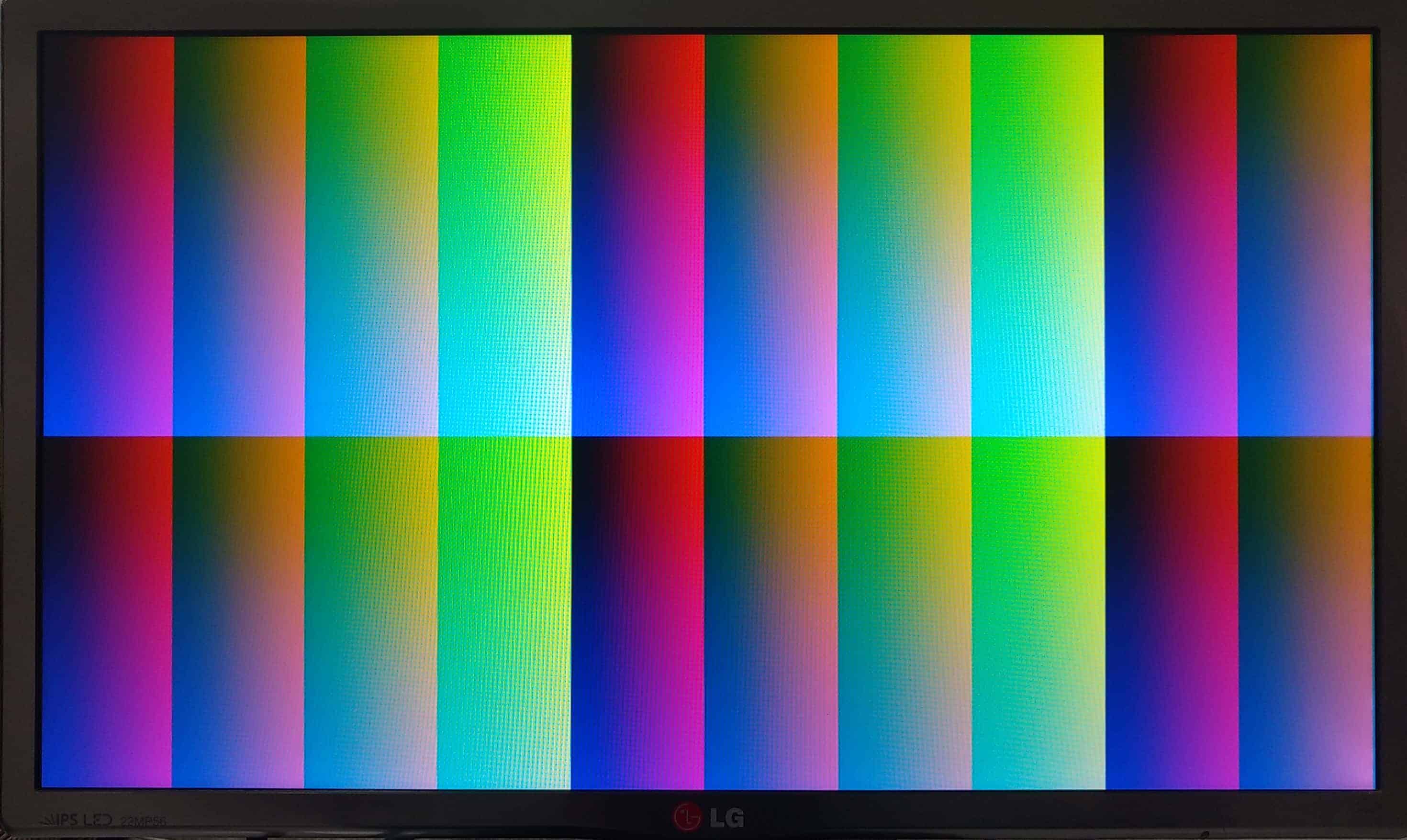
Once MimasA7 is successfully programmed, you will be observing with the color pattern at 640×480@60Hz resolution as shown in the following image.
That was it! You can generate different output pattern for differentvgamodule and also with higher resolution. Congratulations!