Introduction:
HDMI (High-Definition Multimedia Interface) can be viewed as a digital upgrade of VGA standard. It supports high resolution displays as well as audio data embedded along with video. The pixel data in HDMI is serially transferred at ten times of pixel clock frequency using TMDS (Transition Minimized Differential Signalling) to minimize the transitions between 1s and 0s. This article actually demonstrates DVI-D output using Telesto MAX 10 FPGA Module. DVI-D is a subset of HDMI and has same electrical and physical layer implementation as HDMI. So, all HDMI monitors should be capable of receiving the DVI-D signals transported over HDMI cable.
Prerequisites:
- Hardware:
- Telesto MAX 10 FPGA Module
- Saturn IO Breakout Module
- HDMI Expansion Module
- Intel USB Blaster II (optional)
- Software:
- Quartus Prime
- Serial terminal (PuTTY)
Step 1:
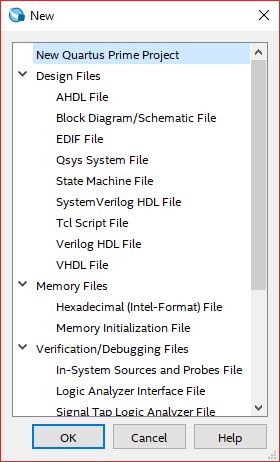
Open Quartus and go to “File” menu -> “New”. Select “New Quartus Prime Project” as shown below and click OK.
Step 2:
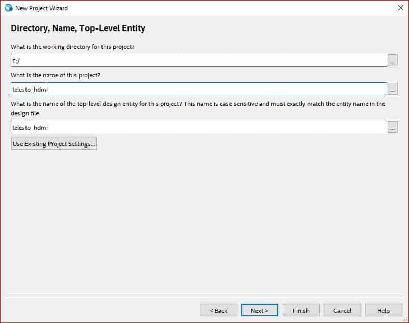
The “New Project Wizard” will open. Click Next. In the “Directory, Name and Top-Level Entity” step, enter a project name of your choice and choose the directory where you want to save the project. Enter the name of top-level module. For this article, the Author used “telesto_hdmi” for both project name and top-level module name.
Step 3:
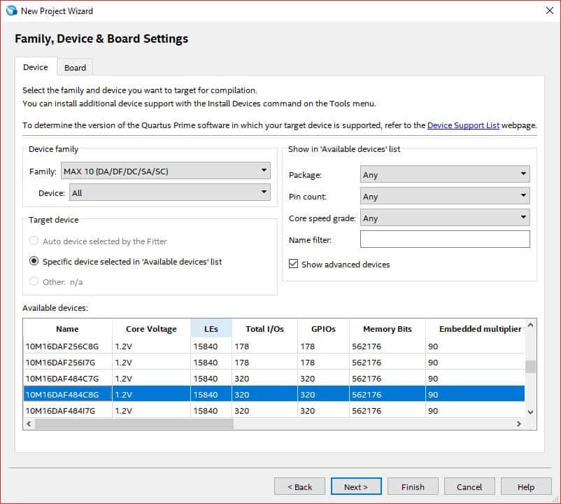
Click Next till you see the ‘Family, Device and Board Settings’ tab. In Boards select ’10M16DAF484C8G’ (select corresponding 10M50 part if your Telesto is of 10M50 variant) and click Next twice and finally Finish.
 Step 4:
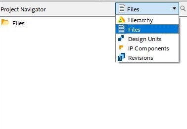
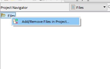
In ‘Project Navigator’, Select ‘Files’ to view all files, then Right-Click ‘Files’ and select ‘Add/Remove files from project’.
Step 5:
Download and extract the RTL source files from here and add them to the project.
The HDMI interface has 3 pairs of differential data signals and 1 pair of differential clock signals:
hdmi_tx [2:0]: These are HDMI/DVI differential signals carrying the video data to be displayed on screen.hdmi_tx_clk: HDMI pixel clock differential signal.
First, VGA signals are generated inside vga_gen & vga_output module. Then the VGA signals are encoded to 10-bits per channel and the data is then serialised to 10x of pixel clock rate. Finally the three channels along with pixel clock are driven out using TMDS differential drivers.
In the top module (hdmi_out), three other submodules are instantiated namely vga_gen, vga_output and vga_to_hdmi. Also, ALT PLL and Altera GPIO Lite IPs are added from IP catalog.
hdmi_out: In this module, ALT PLL IP is used to generate required clocks for VGA and DVI-D. The 100 MHz clock from on-board oscillator is provided as input, and following clocks are derived from it:
pixel_clk:This is the pixel clock frequency for 640×480@60Hz VGA resolution.pixel_clk5: This is 125 MHz clock, used for serialisation in DDIO (Double Data Rate Input/Output).
vga_gen and vga_output: This design generates VGA at 640×480@60 Hz resolution. The vga_gen module generates the timing signals hsync and vsync, while the vga_output module assigns red, green and blue colors components of pixels, thus creating the pixel data.
vga_to_hdmi: VGA signals and clocks are given as input to this module and DVI TMDS signals are generated at the output. It uses a TMDS_encoder module to generate TMDS signals. TMDS uses 8b/10b encoding, the 8-bit color data (red, green & blue) generated by VGA module is converted to 10 bits. These 10-bits of data need to be serialized, for which the ddio_out module is instantiated inside the top module. ddio is an Intel/Altera GPIO Lite IP core which serializes 2-bits of data in one clock cycle of 125 MHz. We need to serialize 10-bits of data produced at 25 MHz, hence serialization is done at five times of of 25 MHz, i.e, 125 MHz. For this serialization, 2-bits of encoded 10-bit data is fetched from vga_to_hdmi module per single clock cycle of the 125 MHz clock.
Step 6:
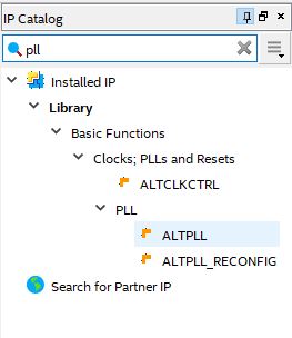
The RTL code added in previous step uses two Altera/Intel IP cores, namely “ALT PLL” IP core and “GPIO Lite” IP core. Add these two IPs from the IP catalog as shown below.
Type pll in IP catalog search box and double-click ‘ALTPLL’
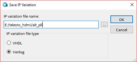
Enter the IP variation file name as ‘alt_pll’ and click OK to open ALTPLL customisation window.
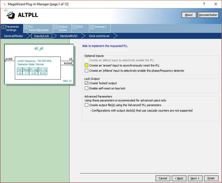
In Parameter Settings tab, de-select “Create an areset input to asynchronously reset the PLL”.
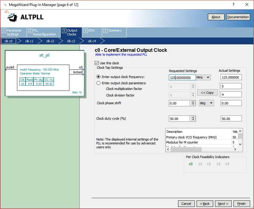
Click Next till you reach ‘Output Clocks’ tab. Enter “clk c0” frequency as 125 MHz and Click Next.
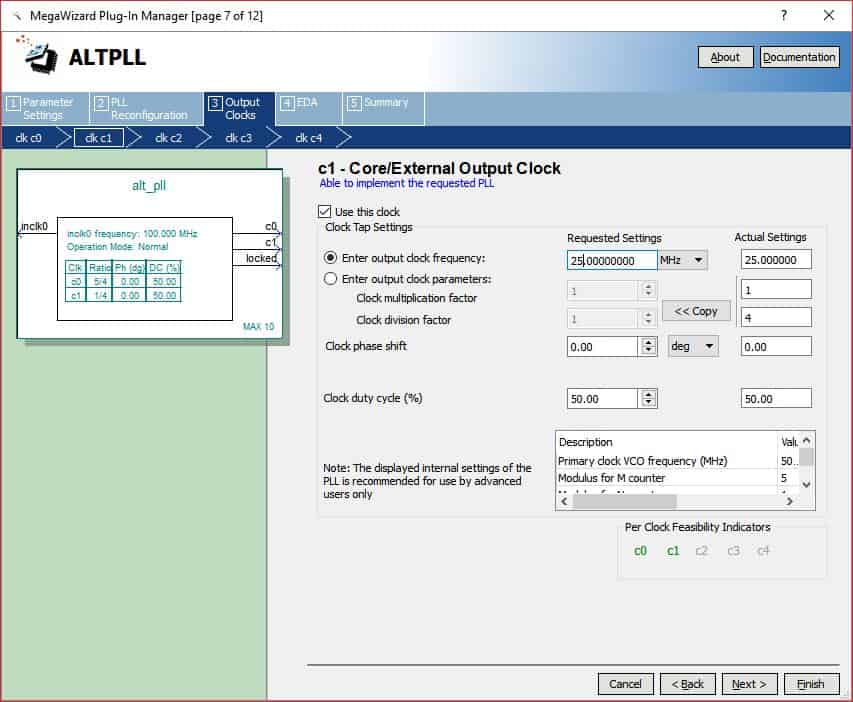
Enter “clk c1” frequency as 25Mhz and Click Finish.
Step 7:
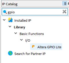
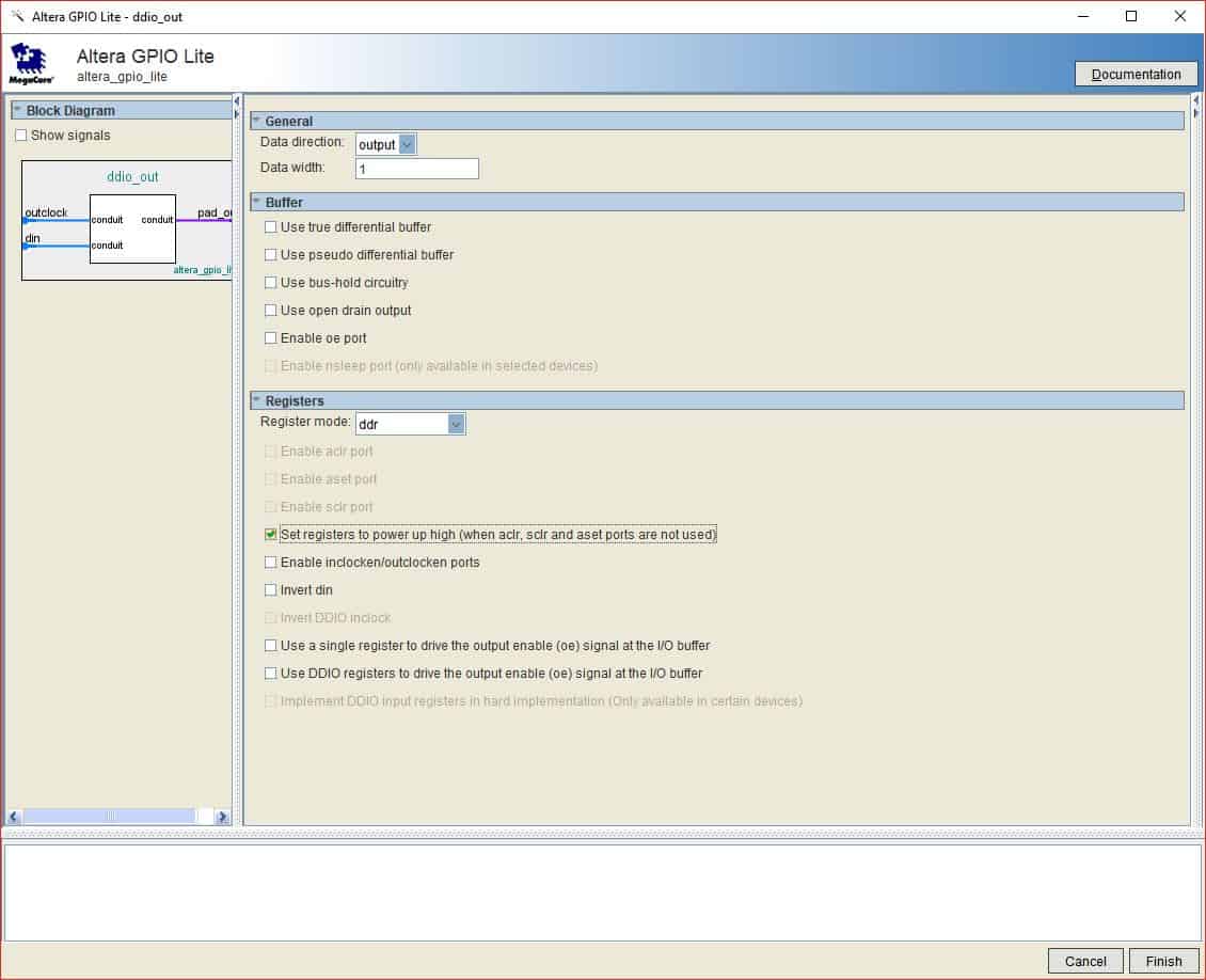
Add ddio IP core by typing ‘gpio’ in IP catalog search box and double-clicking ‘Altera GPIO Lite’.
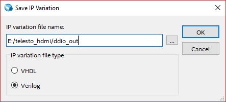
Give the file name as ‘ddio_out’ and click OK to open customisation window.
Select Data width as ‘1’, Register mode as ‘ddr’ and select ‘Set registers to power up high’.
Step 8:
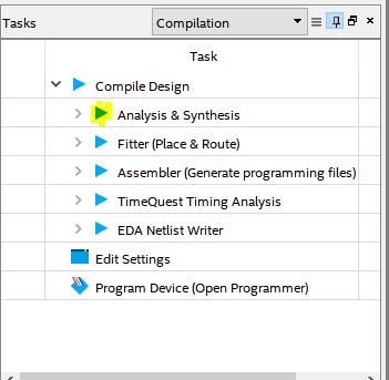
Click on ‘Analysis & Synthesis’ from task menu.
 Step 9:
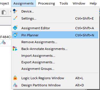
Go to Assignments -> Pin Planner.
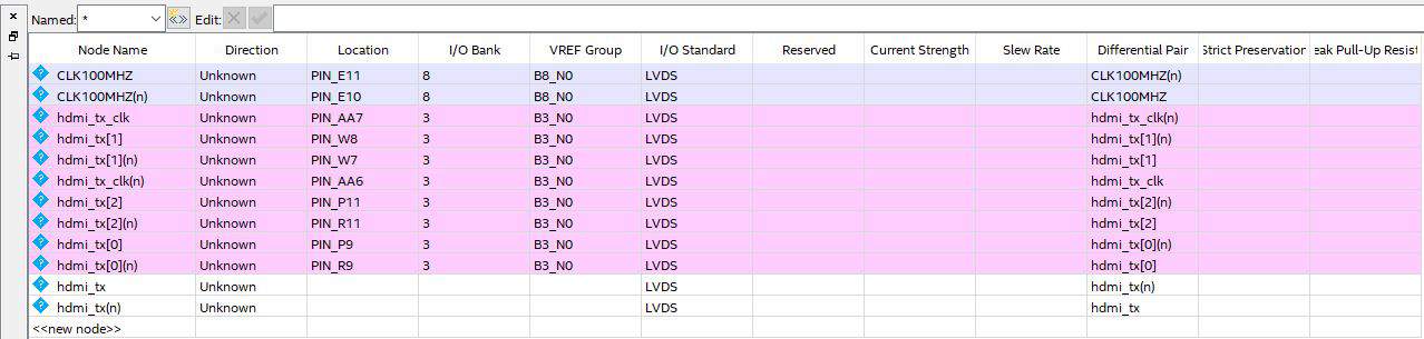
Step 10:
Copy the following pin configurations in your pin planner and close the pin planner.
Step 11:
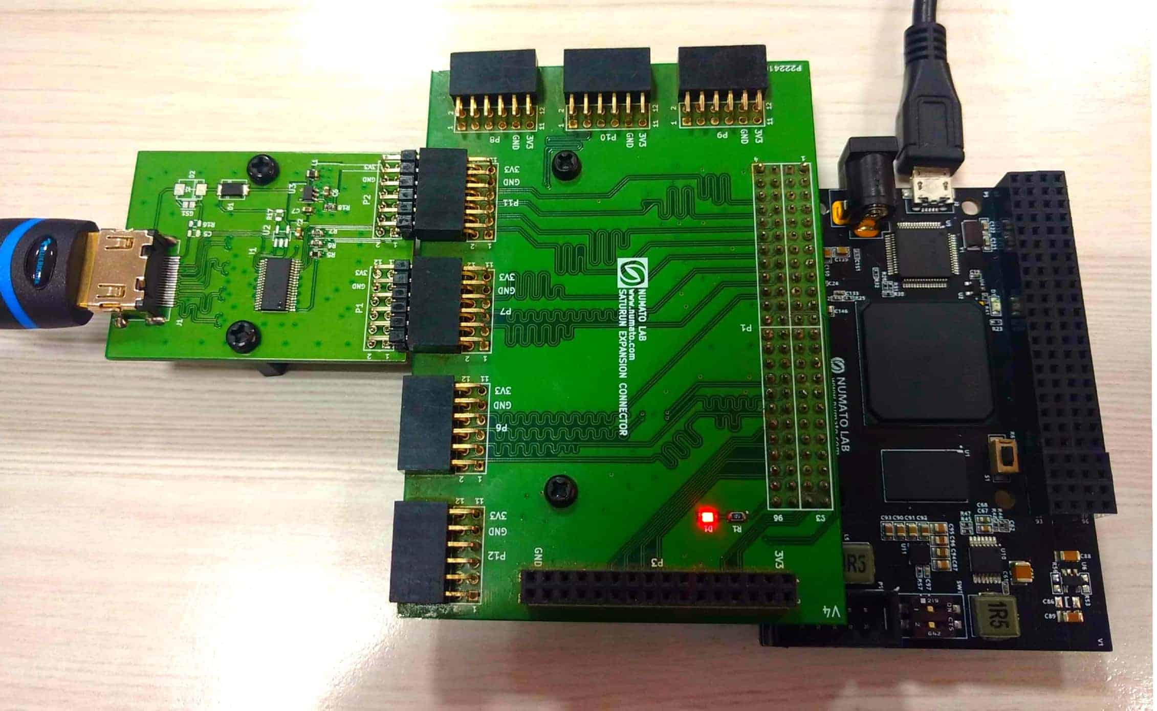
Compile your code again and setup the hardware for testing the design. Connect Saturn Expansion module header P1 to Header P4 of Telesto. Connect HDMI Header P1 and P2 to Header P7 and P11 of expansion module respectively. Connect the HDMI cable between HDMI Expansion module and the monitor. Finally connect the JTAG cable and power supply for Telesto.
Step 12:
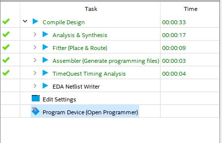
Program the Telesto by clicking Program Device.
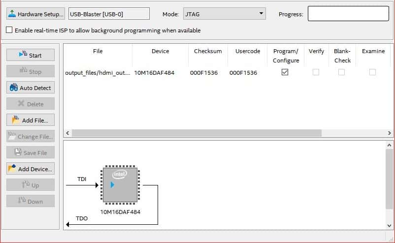
 The Quartus Programmer window will open up. Click “Start” and wait for the device to get programmed.
Step 13:
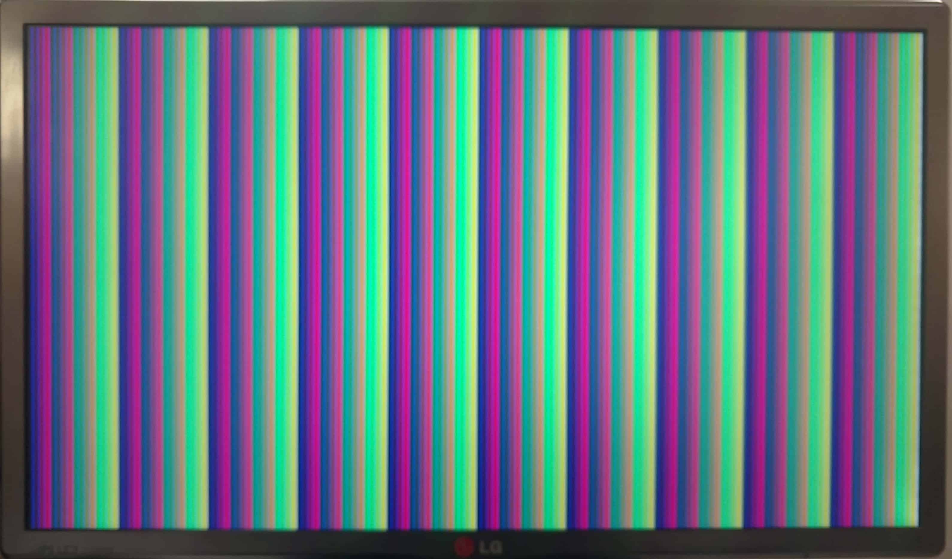
Once Telesto is successfully programmed, it should begin generating HDMI signals and the monitor should display a colorful pattern at 640×480 @ 60Hz resolution, similar to the output as shown below.