Introduction:
This article aims to provide readers with a comprehensive understanding of the process involved in generating a differential Clock output using the Neso Artix 7 FPGA module. Differential Clock signals in FPGA utilize two complementary signals to represent clock transitions, providing improved noise immunity and better signal integrity. This technique helps reduce data errors and enables reliable high-speed communication in FPGA designs
Prerequisites:
Hardware:
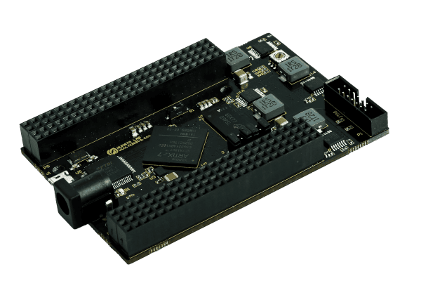
- Neso Artix 7 FPGA Board
- Xilinx Platform Cable USB II JTAG debugger (optional)
Software:
- Xilinx Vivado Suite 2022.1 or newer
- Tenagra FPGA System Management Software
Let’s get started:
Below are the instructions to guide you through the procedure of generating 10MHz clock in Neso.
Step 1:
Download and install Vivado Board Support Package files for Neso Artix 7 from here.
Step 2:
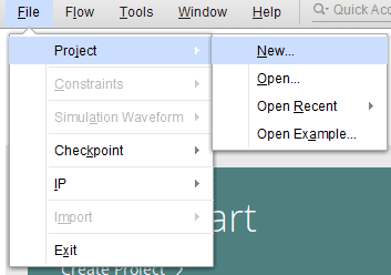
Open Vivado Design Suite, go to File->Project->New. The New Project window will open. Click Next.
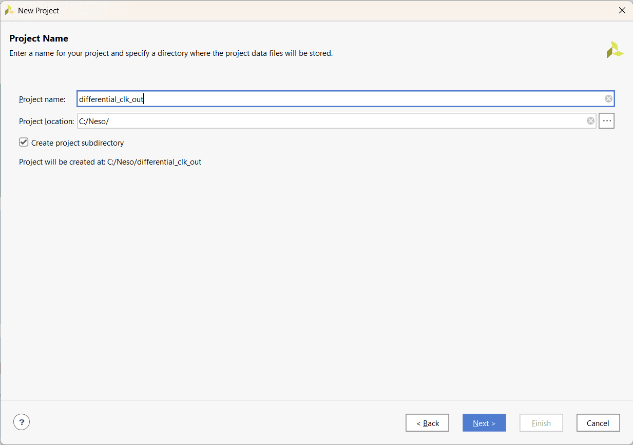
Enter a name for the project and save it at a suitable location. Check the option “Create project subdirectory”. Click Next to continue.
Step 3:
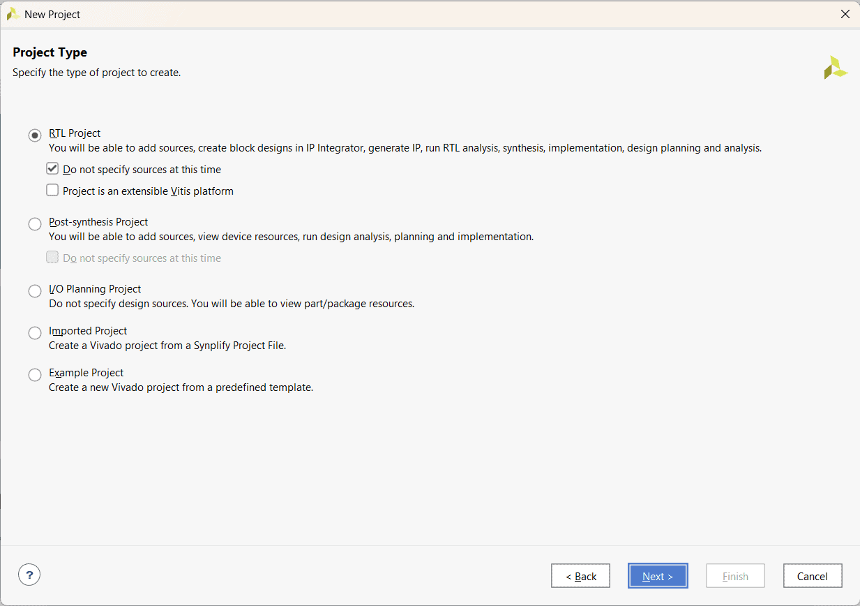
In the Project Type window, select RTL Project and check the “Do not specify sources at this time” option. Click Next.
Step 4:
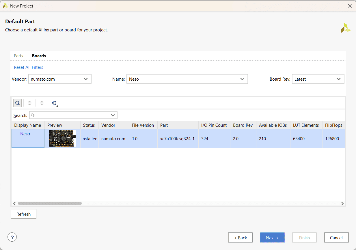
In the Default Part window, select “Neso” from the Boards option. Click Next to continue.
Click Finish to complete creating a new project. Vivado will create a new project with the selected settings.
Step 5:
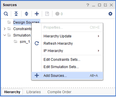
In the Sources tab, right-click on the Design Sources and select Add Sources. It will open a new Add Sources window
Step 6:
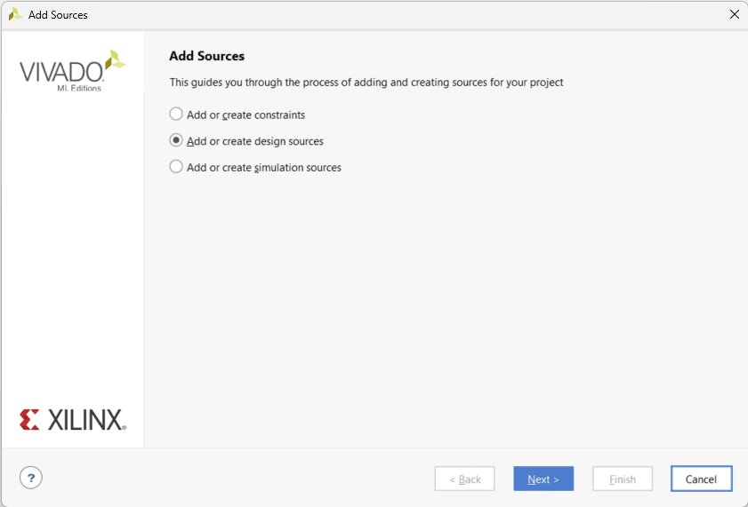
In the Add Source window, select Add or create design source and click Next.
And in the Design or Create Design Source, click on Create File. Select the File type as Verilog and give a suitable File name,
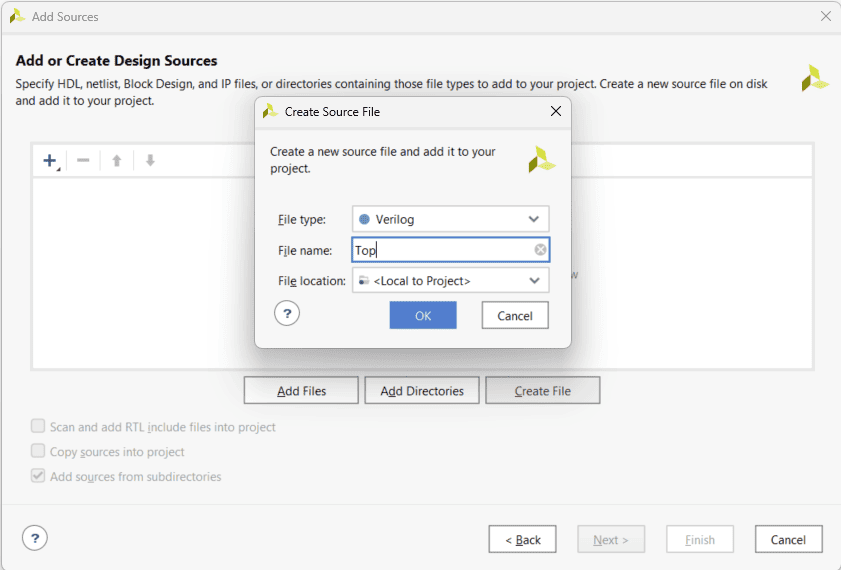
Proceed by clicking OK and then proceed to click Finish .
Step 7:
Copy paste the given code into the newly created Design Source,
module top ( input clk, output clk_out_p, output clk_out_n );

 clk_wiz_0 instance_name
(
  // Clock out ports
   .clk_out1(clk_out), // output clk_out1
  // Clock in ports
   .clk_in1(clk)); // input clk_in1
wire clk_out;
 OBUFDS #(
  .IOSTANDARD("DEFAULT") // Specify the output I/O standard
  // .SLEW("SLOW") // Specify the output slew rate
   ) OBUFDS_inst (
    .O(clk_out_p), // Diff_p output (connect directly to top-level port)
    .OB(clk_out_n), // Diff_n output (connect directly to top-level port)
    .I(clk_out) // Buffer input
  );
endmodule
Step 8:
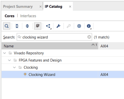
A Clocking wizard is instantiated in the code, so go to “Flow Navigator” panel, click IP Catalog under the “PROJECT MANAGER” section. In the IP Catalog, search for Clocking Wizard IP and double click on it. The “Customize IP” window will open.
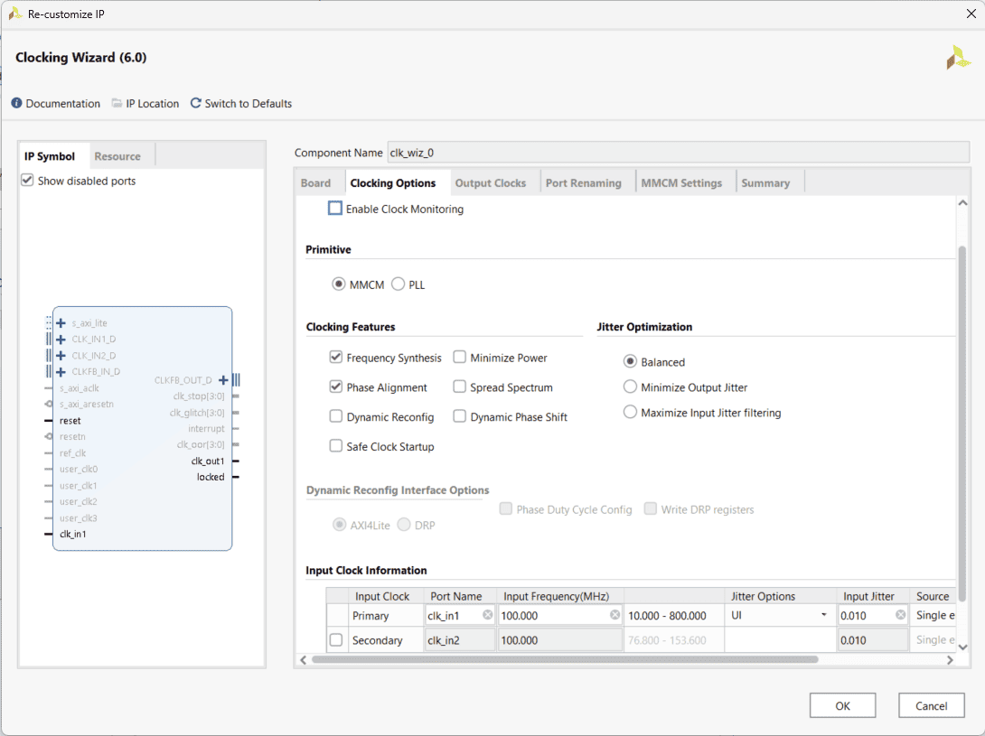
In Clocking Options tab, give Component Name as “clk_wiz_0” and primary clock port name as clk_in1.
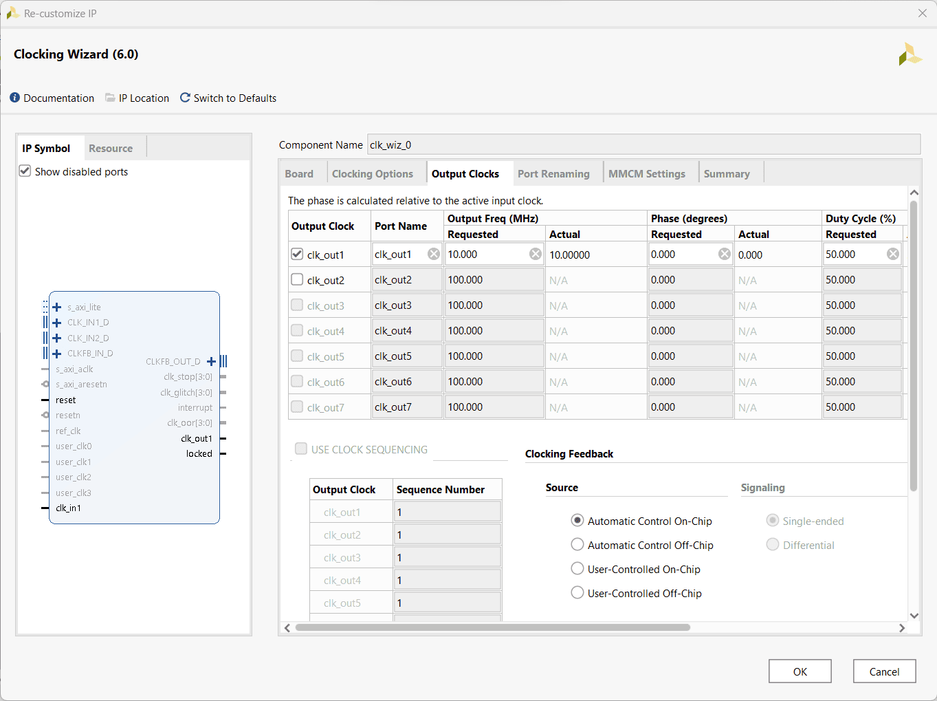
In Output Clocks tab, Provide clk_out1 value as 10MHz and Click OK.
Step 9:
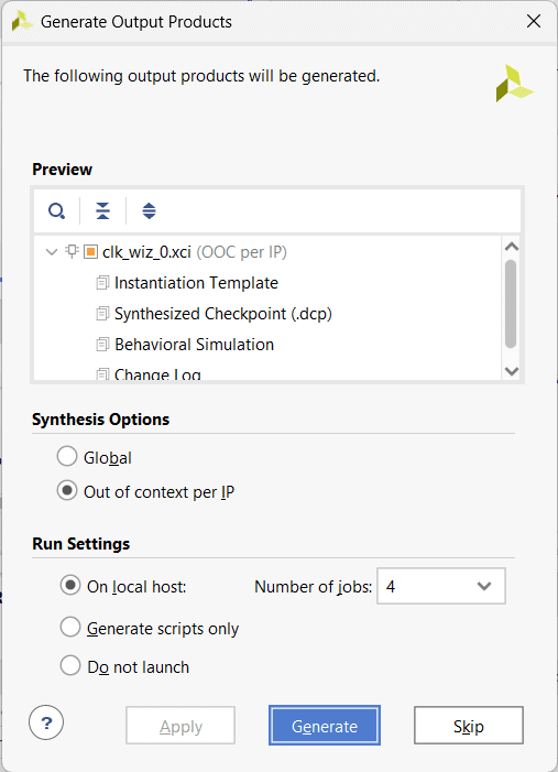
Once the customization is done, generate Output Product Window will pop-up. Click on Generate.
Step 10:
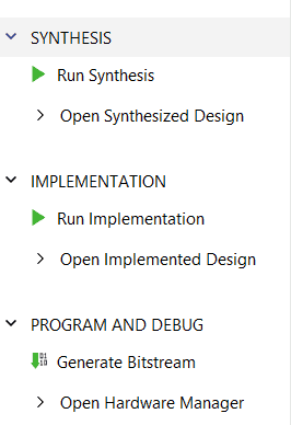
After generating the Output Product, proceed to click on the Run Synthesis option. Once the synthesis process completes successfully without any errors, proceed to click on the Run Implementation option.
Step 11:
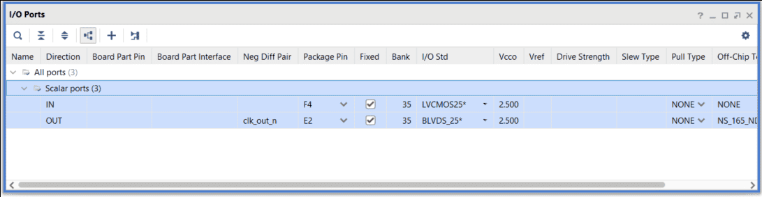
Once the implementation process is complete, proceed to choose the “Open Implementation Design” option. Within the design, navigate to the I/O Ports Tab and accurately specify the appropriate Package name for both the input clock and the output Differential clock pins. It is crucial to provide the correct I/O standard for the scalar ports to ensure accurate communication and compatibility with the chosen package.
Below is the generated constraint file for your reference.
set_property PACKAGE_PIN F4 [get_ports clk]
set_property IOSTANDARD LVCMOS25 [get_ports clk]

set_property PACKAGE_PIN E2 [get_ports clk_out_p]
set_property IOSTANDARD BLVDS_25 [get_ports clk_out_p]
SRCC pins E2 and D2 were selected as the differential pins in this case.
Step 11:
Select Generate Bitstream after a successful Implementation. Once the Bitstream in generated program the board using the bit/bin file. (programming Neso Artix 7 board is available in User manual)
Step 12:
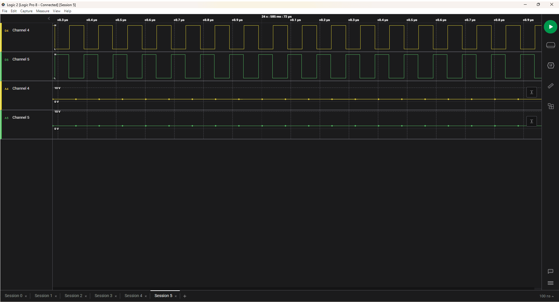
Here is the observed output presented for the reference: