Introduction
PCI Express (Peripheral Component Interconnect Express) is a high-speed serial expansion standard bus. DMA (Direct Memory Access) is a feature that allows peripheral devices to main memory (RAM), independent of the CPU. With PCI Express operating in multi-gigabit data rate and data read from or written to the main memory with the DMA property, the overall performance of the applications is increased exponentially. In this article, we are going to create a simple PCIe DMA example, design and implement it on the Tagus – Artix 7 PCI Express Development Board. We will be controlling LEDs (GPIO) through PCI Express connected to the Host System with Linux and also test DMA functionality.
Prerequisites
Hardware:
- Host PC with Linux or Windows (Linux preferred).
- Tagus – Artix 7 PCI Express Development Board.
- Xilinx Platform Cable USB II (JTAG Cable).
- DC Power Supply (+12V recommended).
Software:
- Vivado 2018.2 or higher.
Creating PCIe DMA Example Design for the Tagus in Vivado
The following steps will walk us through the process of creating a new project, building a PCIe DMA Example Design and program the Tagus using Vivado.
Step 1: Creating a New Project.
Download the Board Support Files (BSP) for the Tagus from here and follow the README.md in the link on how to install the Vivado board files in your system.
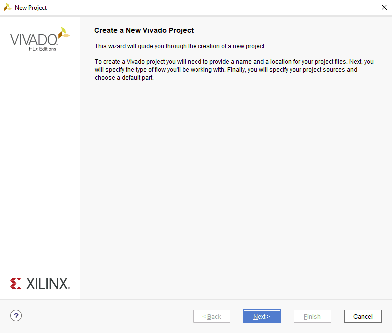
Launch Vivado Design Suite, go to “File->Project->New” to create a new project. The “New project” wizard will pop up. Click “Next” to continue.
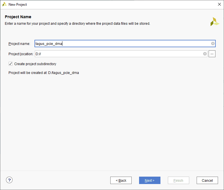
In the “Project Name” wizard, type in a name (for example, “tagus_pcie_dma“) for the project and save it at a convenient location. Select the checkbox below to keep all project files in a single folder. Click “Next” to proceed.
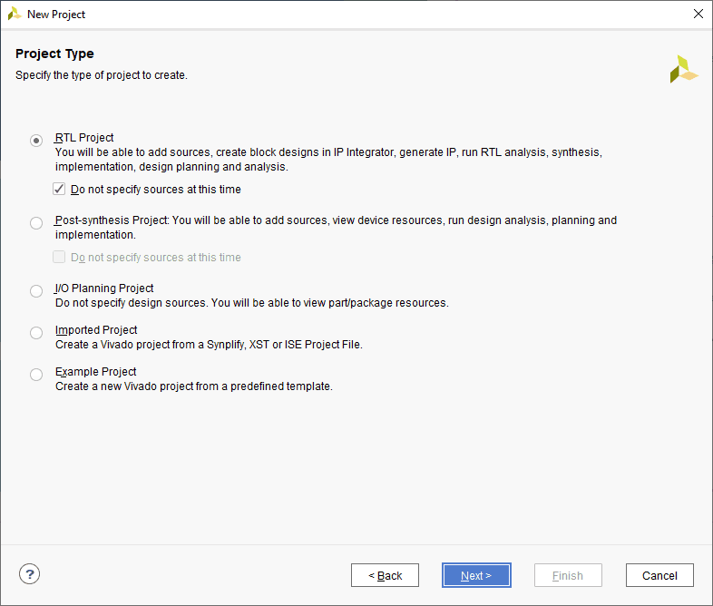
In the “Project type” wizard, select “RTL Project” and select the checkbox to skip specifying the source at the moment. Click “Next”.
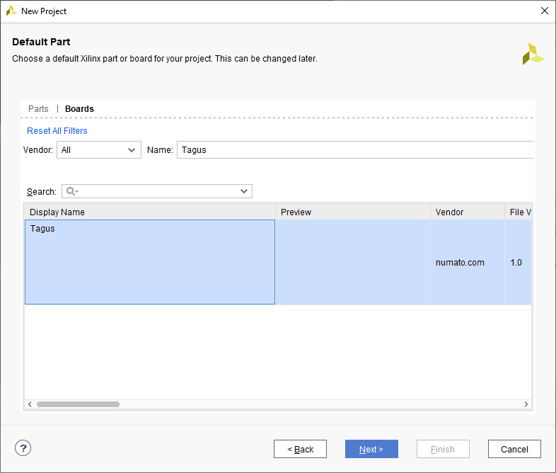
At the “Default Part” wizard, select “Boards” and then select the “Tagus” board. Click “Next” to continue.
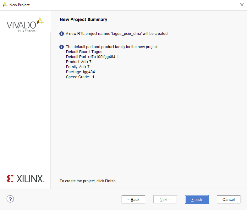
In the next wizard, click “Finish” to create a new project.
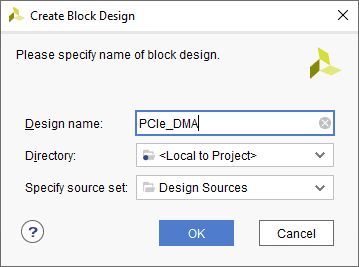
Step 2: Creating a New Block Design
In the “Flow Navigator” panel, select “Create Block Design” under the IP integrator section. Give an appropriate name (Eg: “PCIe_DMA”) to the design and click “OK”.
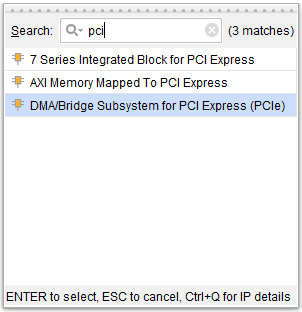
Step 3: Adding & Customizing IP Cores to the Design
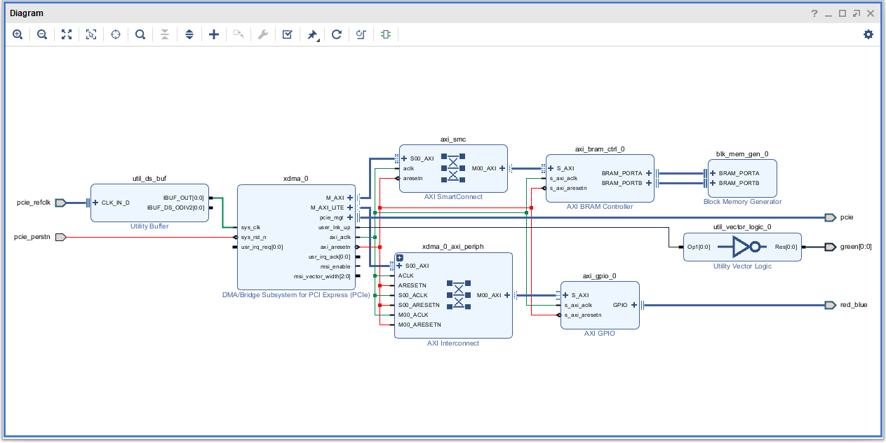
In the Diagram window, right-click and select “Add IP” from the popup menu. Search for “DMA/Bridge Subsystem for PCI Express (PCIe)” and add it to the design by selecting it.
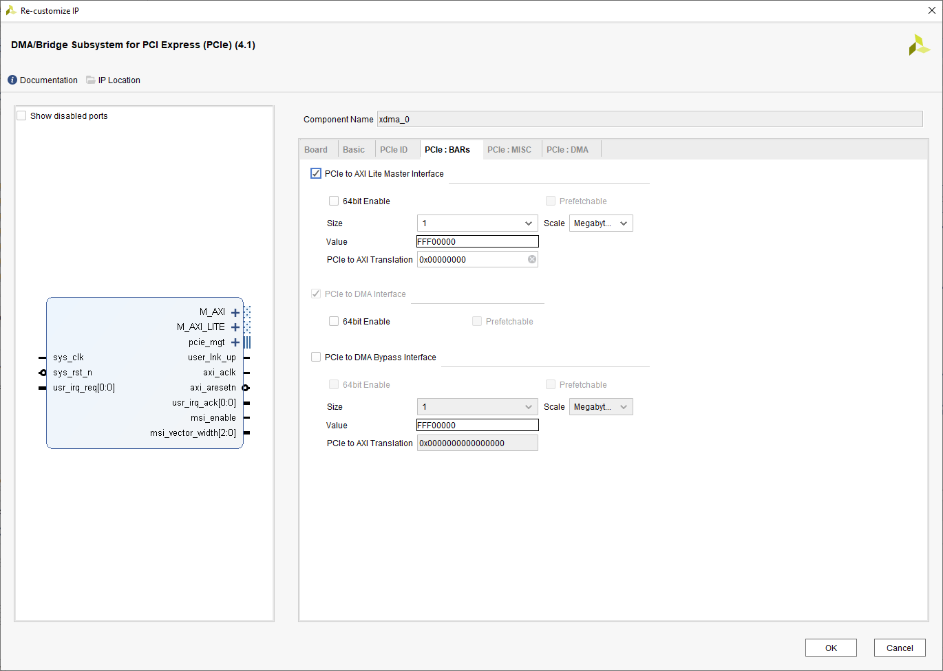
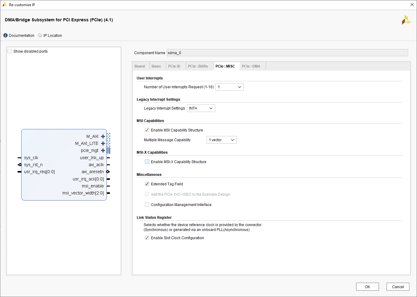
Double click the XDMA (PCIe) IP core to customize it as following
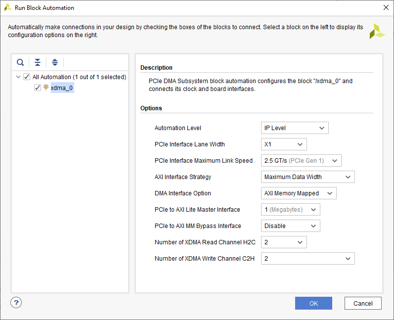
- In the “PCIe: BARs” tab, enable “PCIe to AXI Lite Master Interface” and set the Size Value as “1 Megabyte”.
- In the “PCIe: MISC” tab, disable the “Configuration Management Interface“.
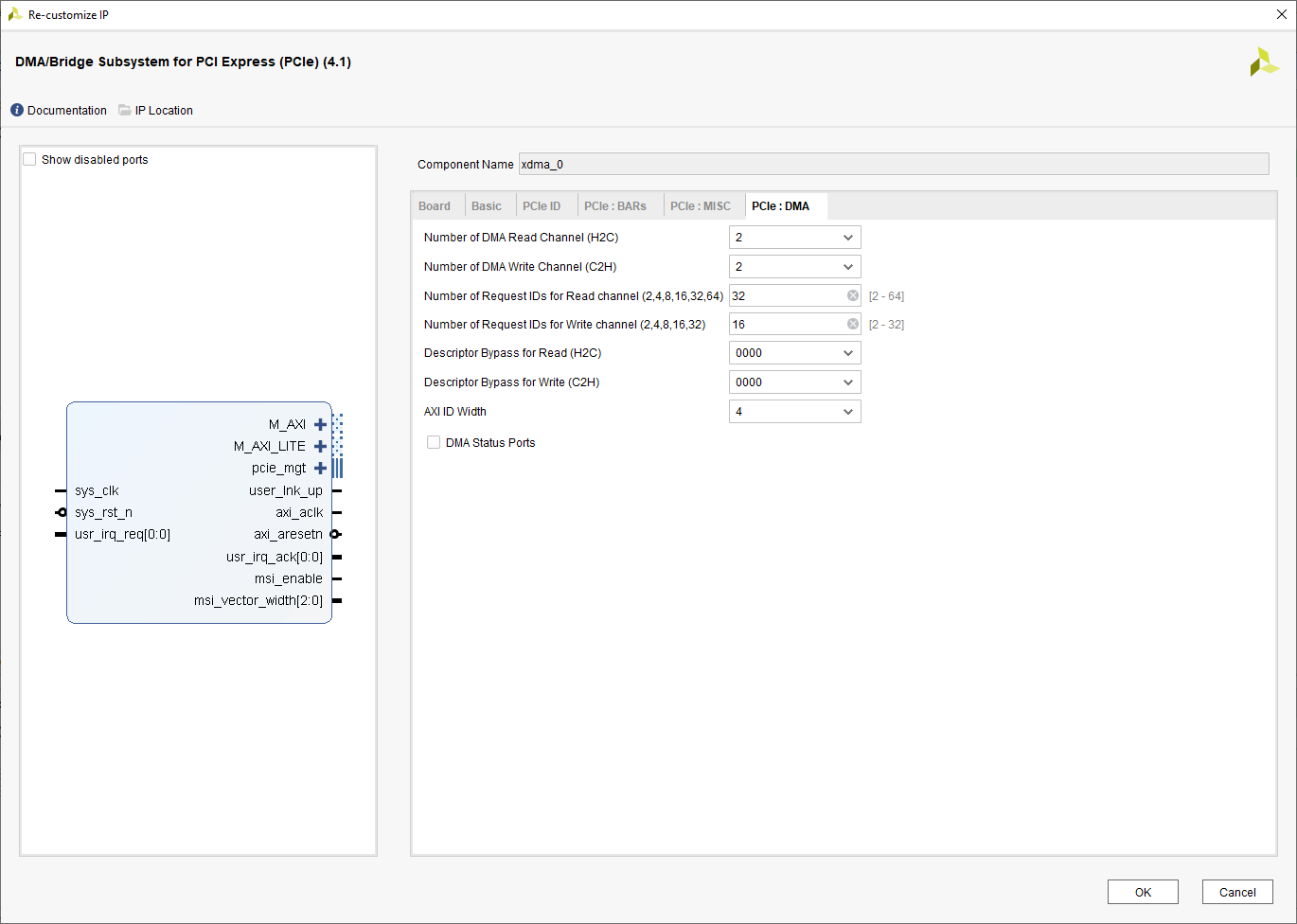
- In the “PCIe: DMA” tab, change the “Number of DMA Read Channels (H2C)” & “Number of DMA Write Channels (C2H)” to 2.
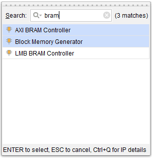
Right-click and select “Add IP”, search for BRAM and add the “AXI BRAM Controller” & “Block Memory Generator” IPs to the design.
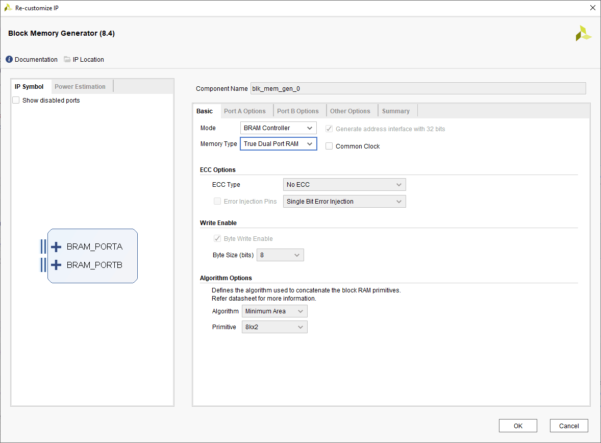
Double click the “Block Memory Generator” IP core to customize it as following.
- In the “Basic” tab, select the Memory Type as “True Dual-Port RAM”.
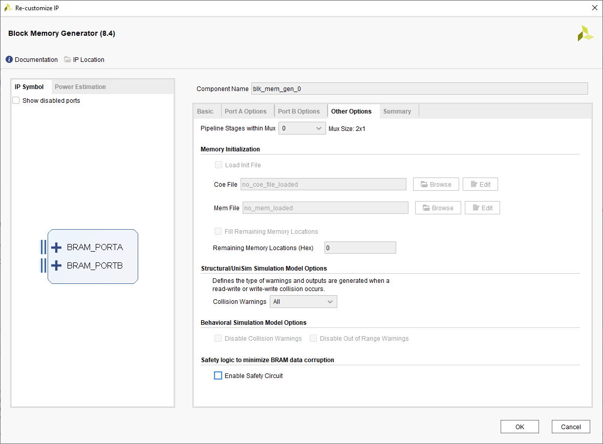
- In the “Other Options” tab, disable the “Enable Safety Circuit”.
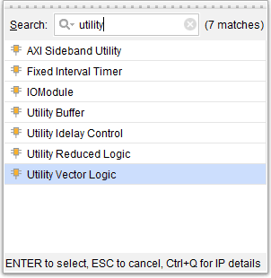
Right-click and select “Add IP”, search for utility and add “Utility Vector Logic” IP to the design.
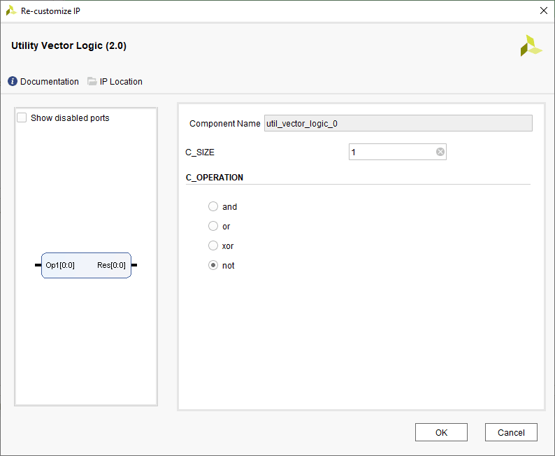
Double click the “Utility Vector Logic” IP core to customize it. Change the “C_OPERATION” to “not” and change the “C_SIZE” to 1 and click “OK” as shown in the image below.
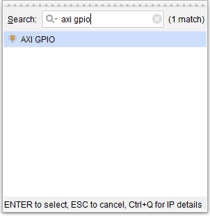
Right-click and select “Add IP”, search and add “AXI GPIO” IP to the design.
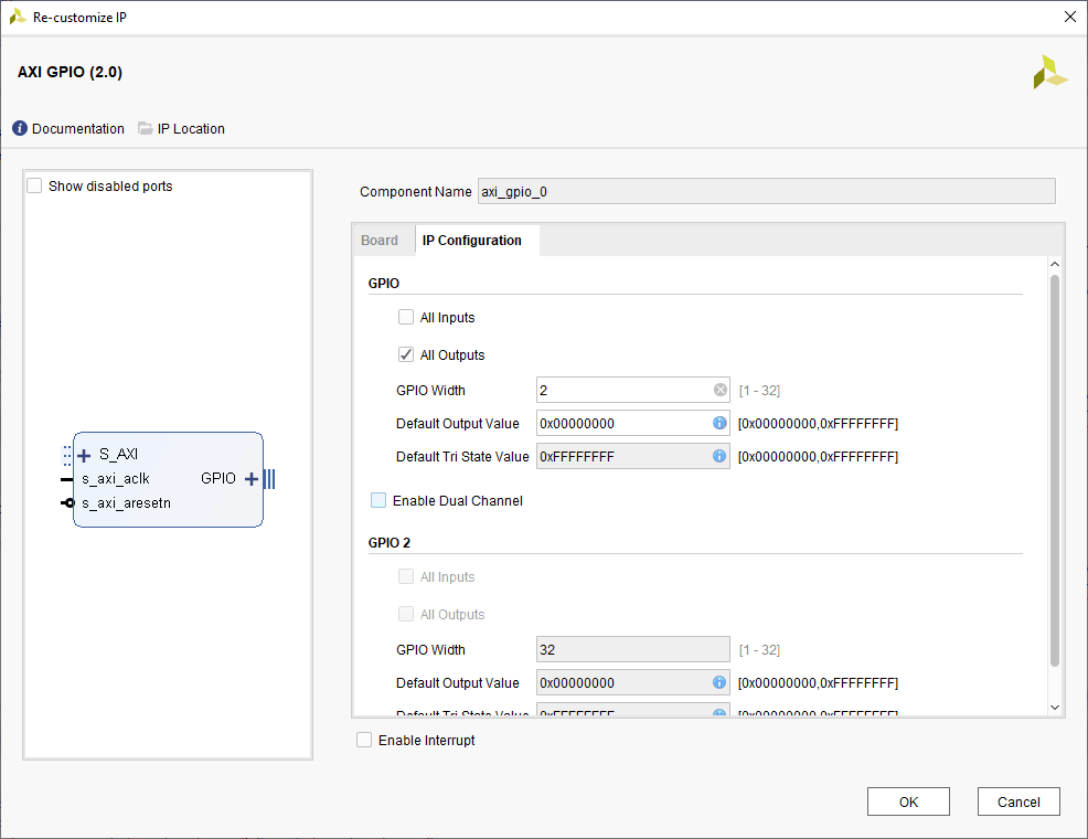
Double click “AXI GPIO” IP core to customize it. In the “IP Configuration” tab, change the ”GPIO Width” to 2 and enable the “All Outputs” option.
Step 4: Run Block Automation, Run Connection Automation & Validate Design
Click “Run Block Automation” present in the “Designer Assistance available” bar on the top left corner of the window to complete the design. Select the settings as shown in the following image. Click “OK” for Vivado to automatically configure the blocks for us.
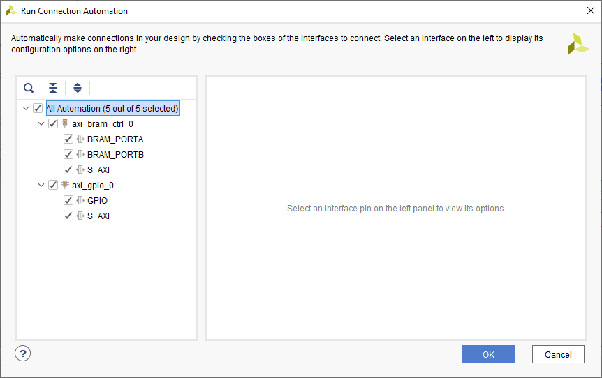
Once the Block Automation is complete, click “Run Connection Automation” so Vivado can connect the blocks to make a complete system.
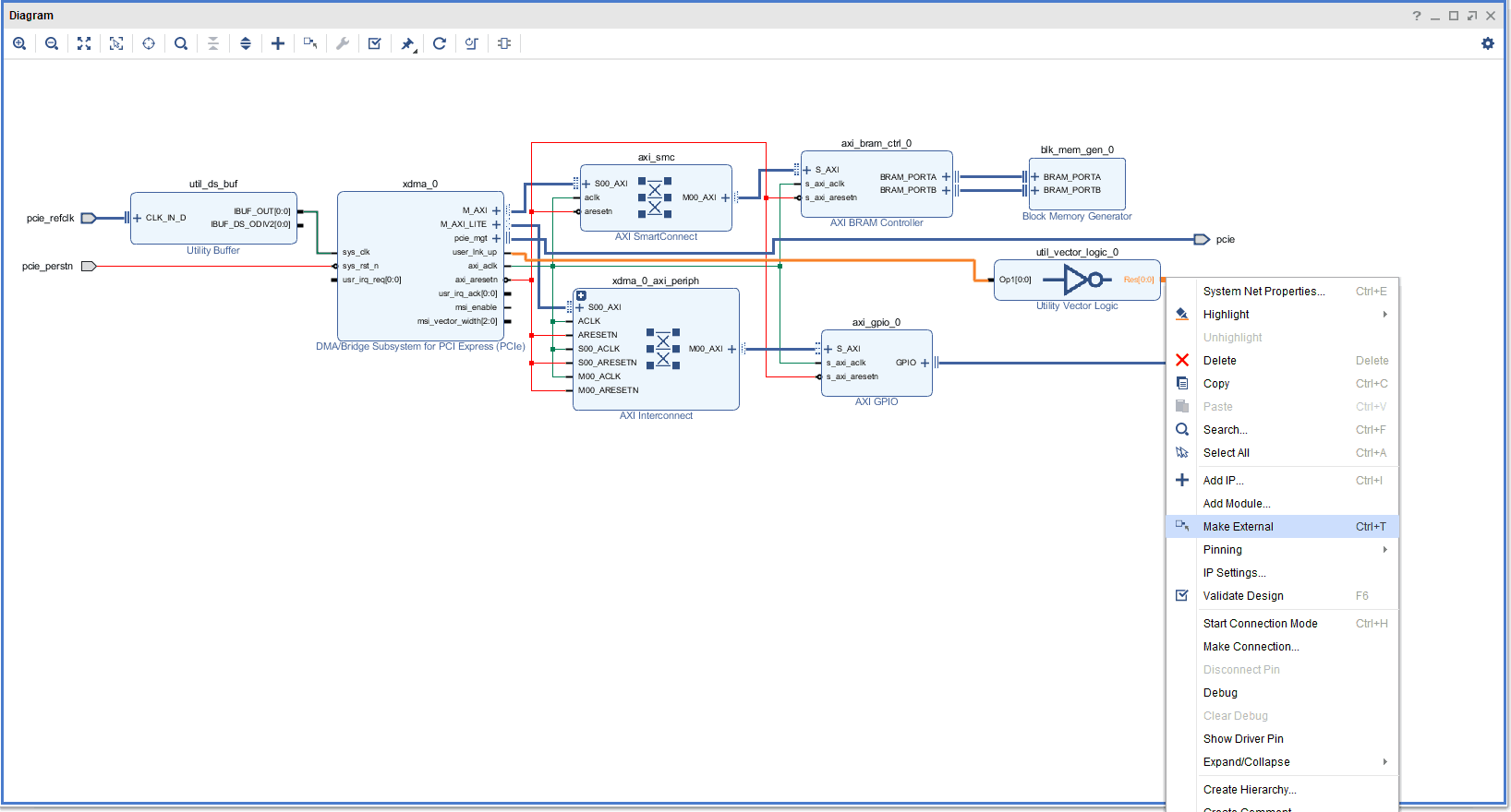
Connect the input of Utility Vector Logic to “user_lnk_up” of “xdma_0” IP and right-click the “Res[0:0]” pin of the Utility Vector Logic IP and select the “Make External” option to make the pin an output signal as shown in the following image. This output port is connected to the Green LED of the board.
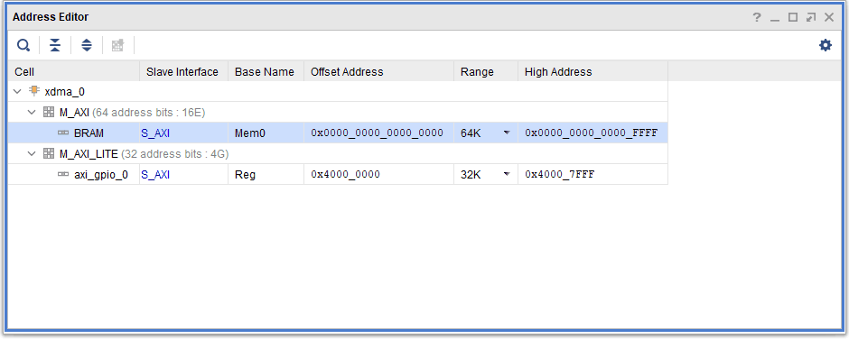
In the “Address Editor” tab, change the Offset Address and Range of axi_bram_ctrl_0 to “0x0000_0000_0000_0000” and “64K” respectively. Also, change the Range of axi_gpio_0 to “32K” as shown in the following image.
Select the “Validate Design” option from the Tools menu to make sure that the connections are correct. The final Block Design should look similar to the following design (change the port names accordingly).
Step 5: Create an HDL Wrapper and Generate Bitstream.
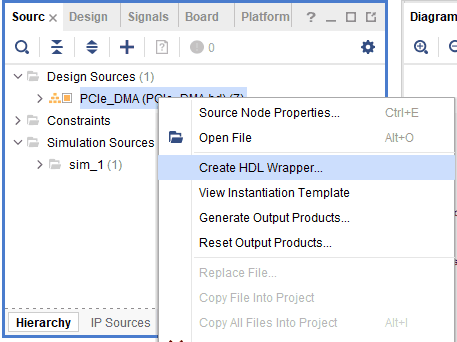
Right-click “PCIe_DMA” in the “Sources” window, select “Create HDL Wrapper” from the popup menu. Click “OK” on the window that appears to finish generating a wrapper.
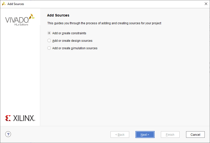
Once the wrapper is complete, we will add constraints for the required ports. Since we have BSP, most of the ports would be assigned from the BSP. For a few ports, we will have to manually assign them. Click “Add Sources” in the Sources window and in the next wizard select “Add or create constraints” and click “Next” to proceed.
Create a constraints file by giving an appropriate name (for example, tagus_pcie_dma) to it and copy the following constraints and paste it into the XDC file.
set_property -dict {PACKAGE_PIN W21 IOSTANDARD LVCMOS33 SLEW FAST} [get_ports {red_blue_tri_o[0]}]
set_property -dict {PACKAGE_PIN W22 IOSTANDARD LVCMOS33 SLEW FAST} [get_ports green]
set_property -dict {PACKAGE_PIN AA20 IOSTANDARD LVCMOS33 SLEW FAST} [get_ports {red_blue_tri_o[1]}]

set_property BITSTREAM.CONFIG.CONFIGRATE 16 [current_design]
set_property BITSTREAM.GENERAL.COMPRESS TRUE [current_design]
set_property BITSTREAM.CONFIG.SPI_BUSWIDTH 4 [current_design]
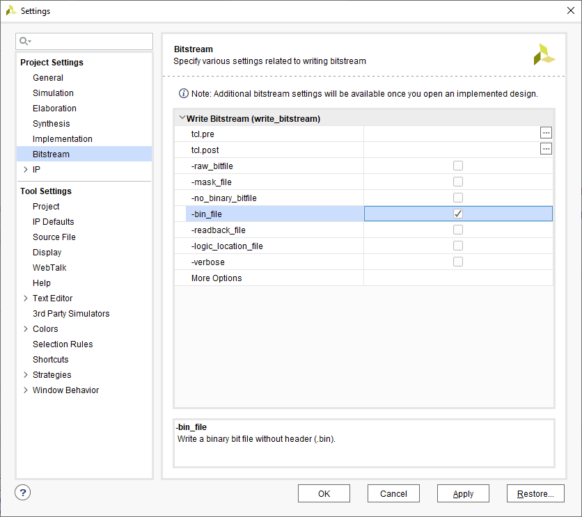
Right-click on “Generate Bitstream” under “PROGRAM AND DEBUG” in the “Flow Navigator” panel and select “Bitstream Settings”. Enable the “-bin_file” checkbox and click “OK“.
Click “Generate Bitstream” to synthesize, implement and generate a bitstream. This process will take some time to complete (around 20-30 minutes). Once the bitstream generation is completed, select “Open Hardware Manager” and click “OK“.
Step 6: Programming Tagus with generated bitstream
Program the Tagus by following the steps “Programming QSPI Flash using Vivado” available in the Product user manual.
Communicating with the Tagus via PCI Express on Linux Machine:
The following steps are implemented on the Host System with Linux. If you wish to implement on Windows Host System, follow the “Communicating with the Tagus via PCI Express on Windows Machines:” section in this article for GPIO control and follow the Xilinx Answer 65444 for DMA.
To control the GPIOs (RGB LED connected in the design):
Step 1:
Connect the Tagus Board in PCIe Slot and boot the Linux system. Open Terminal and check whether PCIe is connected by executing the command lspci -vv.
If the host is unable to detect Tagus (which should show up as “Serial controller: Xilinx Corporation Device 7011” as in the image below), make sure the board is inserted correctly into PCIe Slot and do a soft reset after the host is powered up. A soft-reset after the host is powered up helps the host detect FPGA-based PCIe devices.
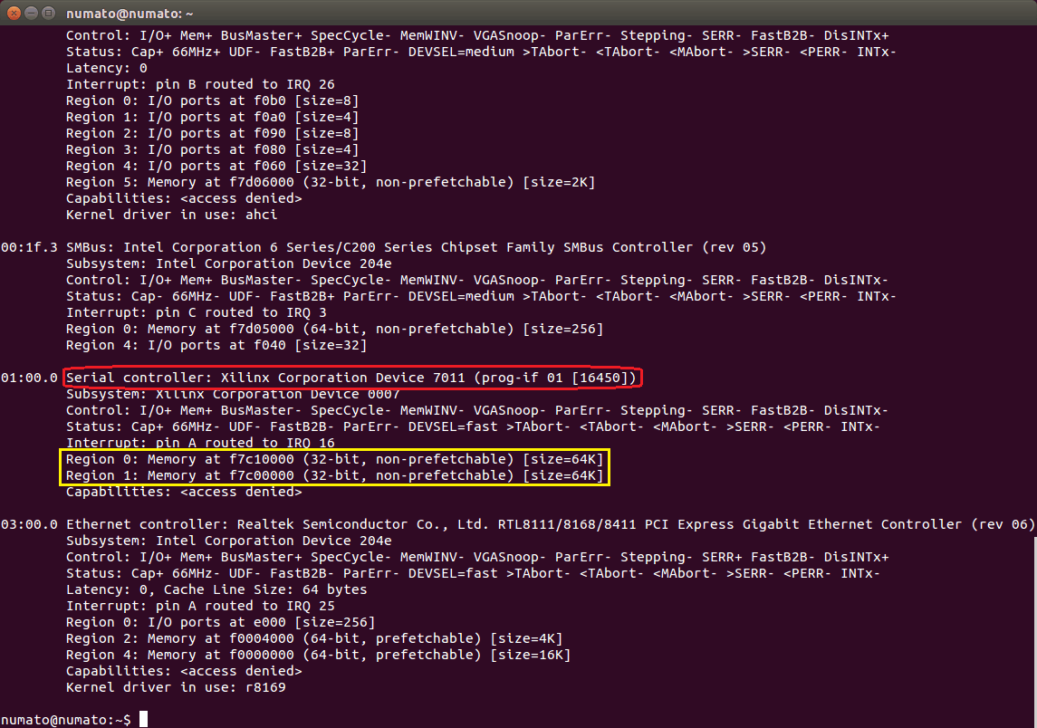
We can observe the PCIe base addresses in the above image. Download the complete pcimem application code zip file and unzip it in a specific location.
Step 2:
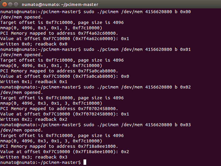
In the command-line terminal, change the directory to where the “pciemem” code is saved. First, compile the C program by executing the command make. Once it is compiled successfully, use the following command:
sudo ./pcimem /dev/mem 4156620800 b 0x00
Here,
4156620800: indicates the base address + offset, it is the address to which write is performed and it is the decimal value of hex: 0xf7c10000 .
b: indicates whether it is word [w], byte [b] or half-word [h].
0x00: 8-bit data value for write purpose.
We can observe the following output indicating that the last 2 bits of data have been written to the specified address and read back from it. If the written data matches the data read, it means data was successfully written to the Tagus and we will be able to observe the output on the LEDs. Here, the last 2 bits are taken for the output on Red & Blue LEDs.
To check the DMA functionality:
Step 1:
Connect the Tagus Board in the PCIe Slot and boot the Linux system. Open Terminal and check whether PCIe is connected by executing the command lspci -vv.
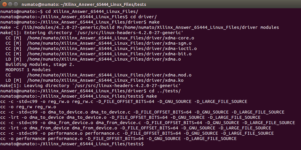
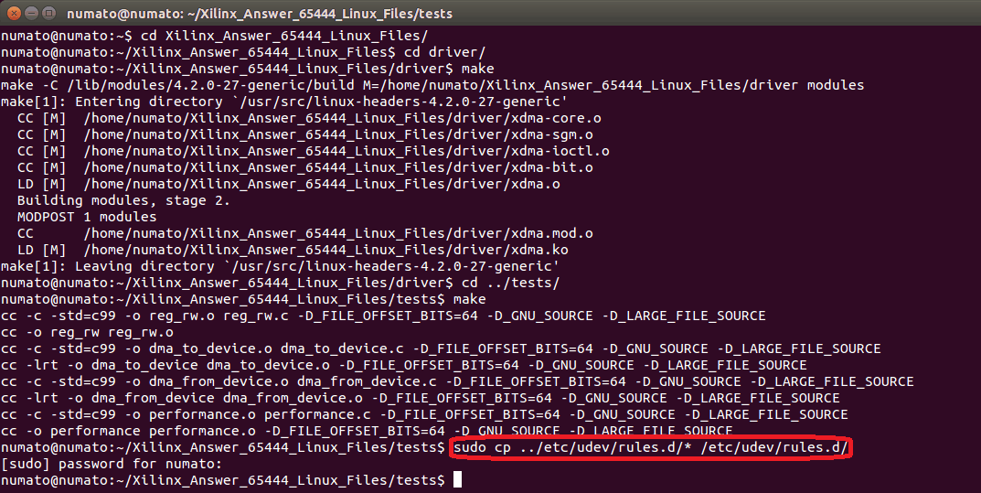
Download the Xilinx Answer 65444 for Linux System from here and save it in a specific location. In the command-line terminal, change the directory to the “Xilinx_Answer_65444_Linux_Files” folder. Enter the /Xilinx_Answer_65444_Linux_Files/driver/ folder by executing the command cd driver/ and compile the C program by executing the command make. Once the compilation is completed, change the directory to the /Xilinx_Answer_65444_Linux_Files/tests/ folder by executing the command cd ../tests/ and execute the make command to compile the C program in the folder.
We will copy the driver rules to the /etc/ directory of the system by executing the following command:
sudo cp ../etc/udev/rules.d/* /etc/udev/rules.d/
Enter the Linux system password, if asked.
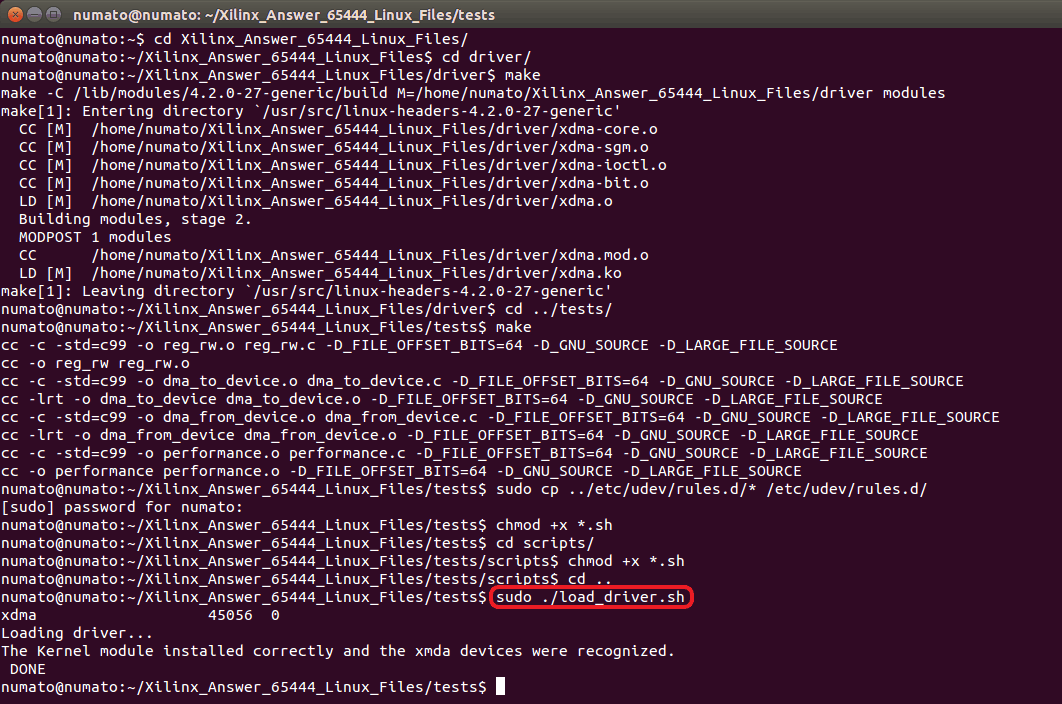
Step 2:
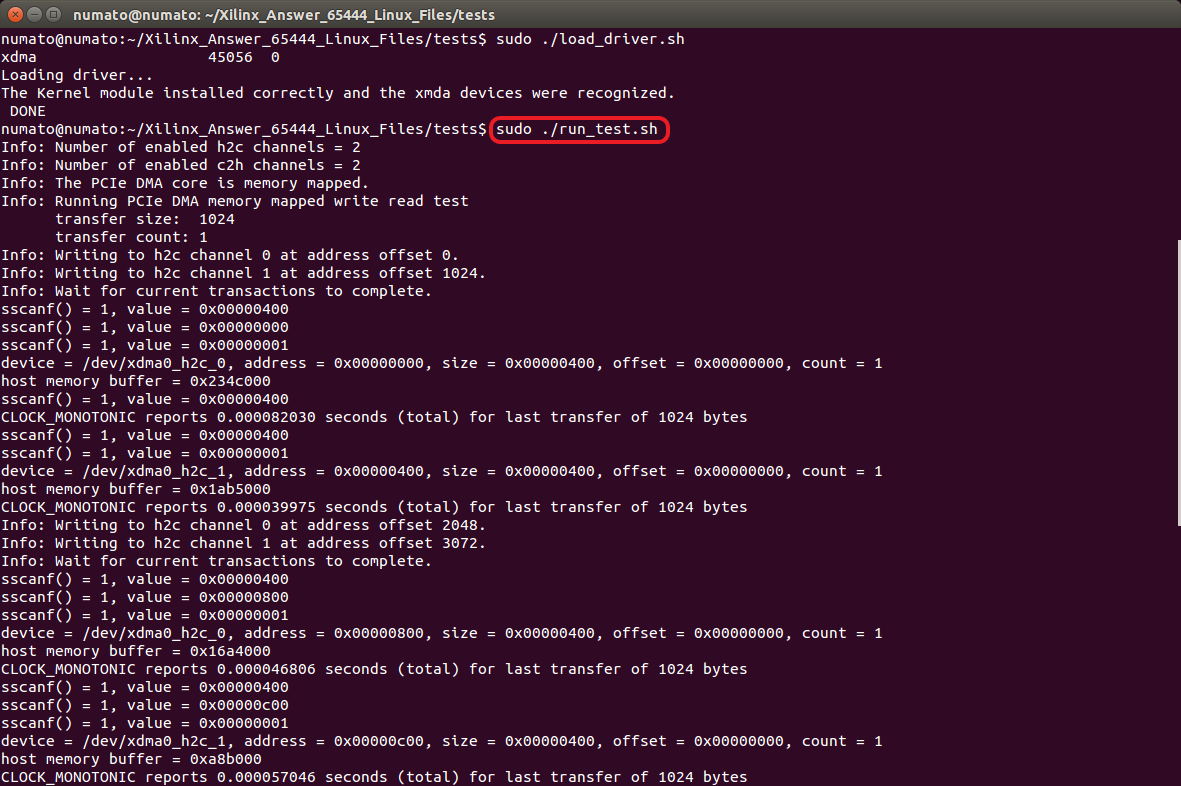
Load the driver by executing the following command:
sudo ./load_driver.sh
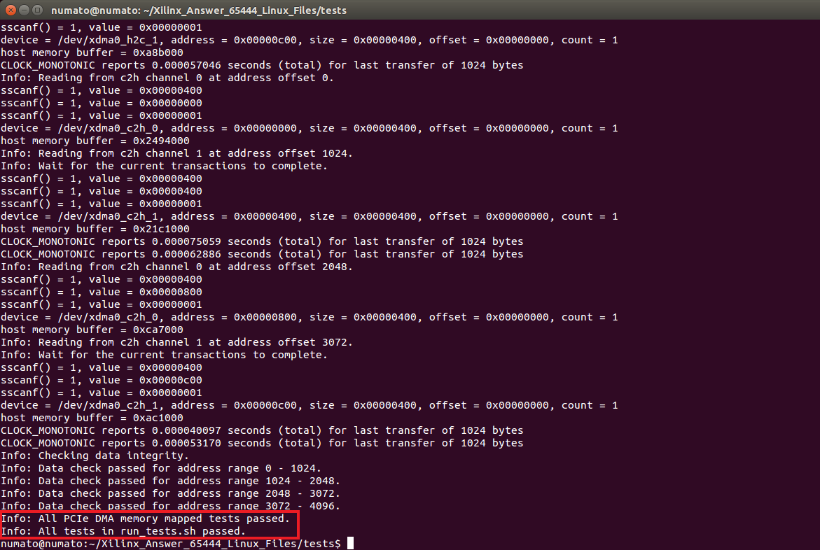
Once the driver is loaded, we can run the DMA test by running the shell file “run_test.sh” by executing the command:
sudo ./run_test.sh