Introduction
Styx Zynq Module features a Zynq 7020 from Xilinx in CLG484 package. The unique feature of Zynq-7000 series is that they are complete System on Chip (SoC) with an FPGA die which makes it a very powerful combination. Styx Zynq Module comes in the same form factor as our Saturn Spartan 6 FPGA Module and so allows for a seamless upgrade in most cases.
One difference between Saturn vs Styx which one might notice is in the clock oscillators of both modules: Saturn has 100MHz clock oscillator whereas Styx has 33.33MHz clock oscillator. This is not where the difference ends. On Saturn, the clock is directly connected to FPGA’s GCLK pin allowing for the designs to directly use the clock by specifying the clock’s location in the user constraints file. On the other hand, Styx has a quite different clocking mechanism due to which we cannot directly assign a clock pin location in user constraints file. The 33.33MHz clock is connected to the hard-silicon part of Zynq SoC and drives different PLLs from which all clocks for the SoC core and its peripherals are derived. The Programmable Logic (PL) section of Zynq can also source a total of 4 different clocks from this clocking hardware.
In this article, we will see how to generate a 100MHz clock from the PS (Processing System) section of Zynq and use in FPGA fabric.
Prerequisites:
This article assumes you have access to the following:
- Xilinx Vivado Design Suite 2016.1 or higher
- Styx Zynq FPGA Module
- Xilinx Platform Cable USB II JTAG
Description
The 33.33MHz clock on Styx module is connected to the hard-silicon part of Zynq SoC at Pin location F7 (on CLG484 package) named PS_CLK (Processing System Clock). This clock drives an elaborate clocking hardware inside the Zynq SoC as shown in the image below:
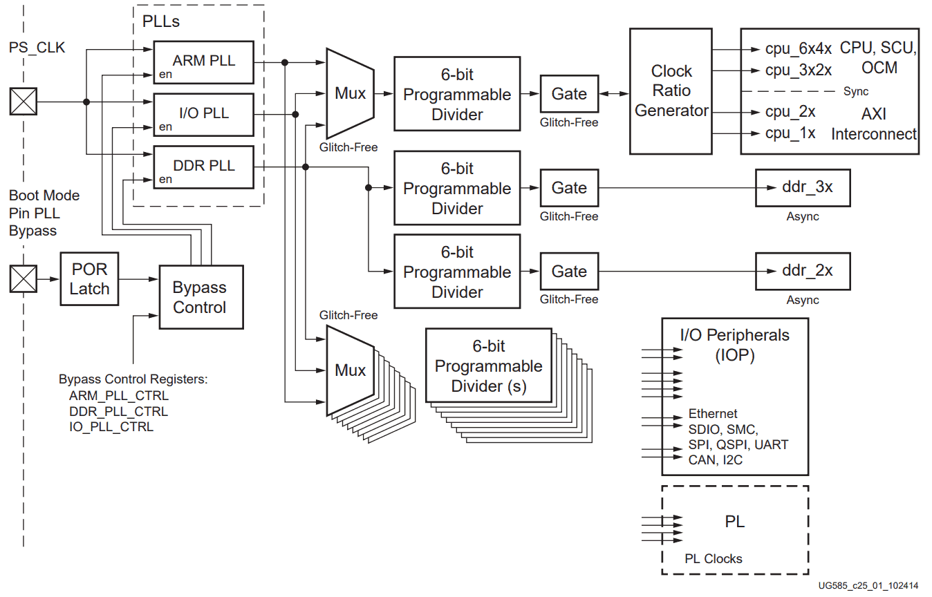
Zynq PS Clock System Block Diagram, Source: Zynq TRM, Copyright: Xilinx, Inc
In the bottom right corner of the above image, you can see that Programmable Logic(PL, i.e the FPGA) section of the Zynq SoC has 4 clocks available from the clocking hardware. Each of these clocks has independent paths and are assumed to be totally asynchronous to each other. Each of these 4 clocks is sourced from either of the 3 PLLs, via a glitch-free multiplexer, and then pass through a 6-bit programmable frequency divider, and finally go into the PL section Zynq SoC.
We can utilize this clocking hardware to generate clocks for use in our HDL designs running on PL section of Zynq. Rest of this article will attempt to explain how to do this practically.
Here is what we are going to do:
- We will take a Verilog design which requires a 100MHz clock to work as per its specification. This could be a design which was created for Saturn for example, and now we need to upgrade to Styx.
- Use Vivado to configure and generate a 100MHz clock from Zynq PS IP block.
- Finally, we will use the 100MHz clock sourced from Zynq PS as the clock input for our Verilog module.
Steps
Step 1
Create a new project named “styxClockTest” for Styx board in Vivado. Follow steps 1 to 5 of this article to create a new project targeted specifically for Styx Board using Numato Lab’s Vivado Board Support files for Styx.
Step 2
Press “Alt+A” key combination. This will bring up “Add Sources” window. Choose “Add or create design sources” and click “Next”. In the next step, click “Create File” and enter in the name of the file as “squarewave.v”. Click “OK” and then “Finish”.
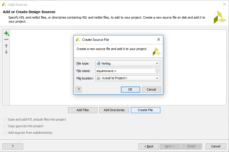
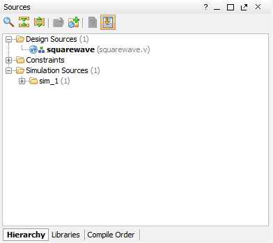
A new dialog window “Define Module” will pop up. Just click “OK” followed by “Yes” for the questions asked. The new source file will be listed in the “Sources” tab.
Step 3
Open the squarewave.v file in the Vivado editor by double-clicking it from the sources window. Select all text created by Vivado and delete it. The squarewave.v file should be blank now. Next, copy the complete below Verilog code into the squarewave.v file and save it.
`timescale 1ns / 1ps

module square_wave_gen(
	input clk,
	input rst_n,
	output sq_wave
);

	// Input clock is 100MHz
	localparam CLOCK_FREQUENCY = 100000000;

	// Counter for toggling of clock
	integer counter = 0;

	reg sq_wave_reg = 0;
	assign sq_wave = sq_wave_reg;

 always @(posedge clk) begin

		if (!rst_n) begin
			counter <= 8'h00;
			sq_wave_reg	 <= 1'b0;
		end

		else begin

			// If counter is zero, toggle sq_wave_reg
			if (counter == 8'h00) begin
				sq_wave_reg <= ~sq_wave_reg;

				// Generate 1Hz Frequency
				counter <= CLOCK_FREQUENCY/2 - 1;
			end

			// Else count down
			else
				counter <= counter - 1;
			end
		end

endmodule
The above code generates a Square Wave of frequency 1Hz. It assumes an input clock to be of 100MHz. So, we need to provide a 100MHz clk input to this Verilog module. We will do that later in this article.
Step 4
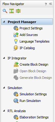
Under “Flow Navigator”, click “Create Block Design”
Name the block design as “styx” and click “OK”
Step 5
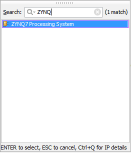
Go to Diagram window, right click and select “Add IP” from the popup menu. Search for ZYNQ7 Processing System. Add ZYNQ7 Processing System to block design by double-clicking. A Zynq7 Processing System IP block will be added in the block design.
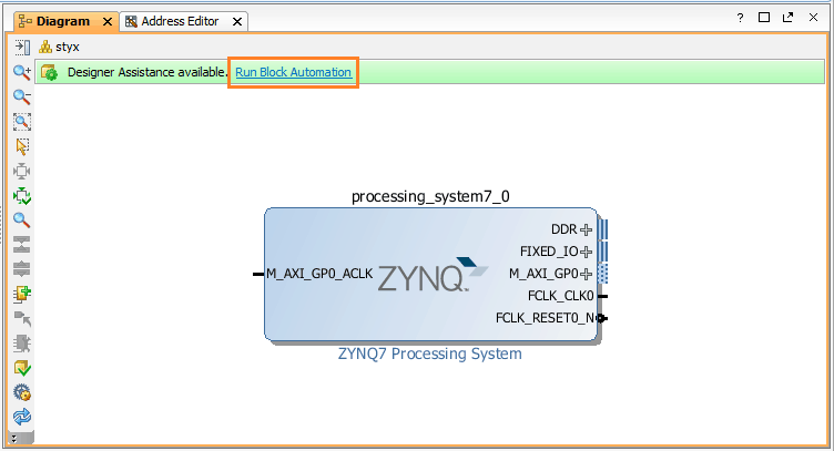
Step 6
Click on “Run Block Automation” option on the green bar.
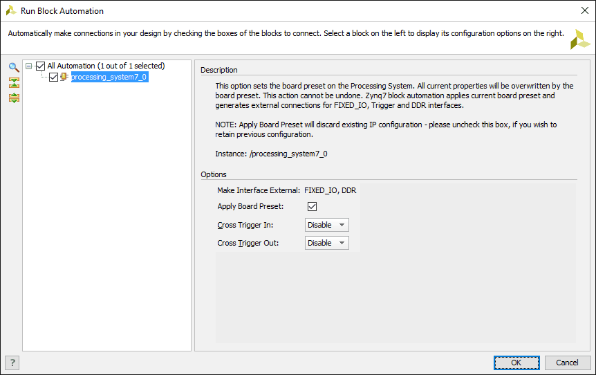
Step 7
In the “Run Block Automation” window, leave the default options as in image below and click OK.
When Block Automation is executed, Vivado will use the settings in the Board Support files for Styx provided by Numato Lab to configure the FCLK_CLK0 clock for 100MHz frequency. We can now use this clock for our RTL designs.
Step 8
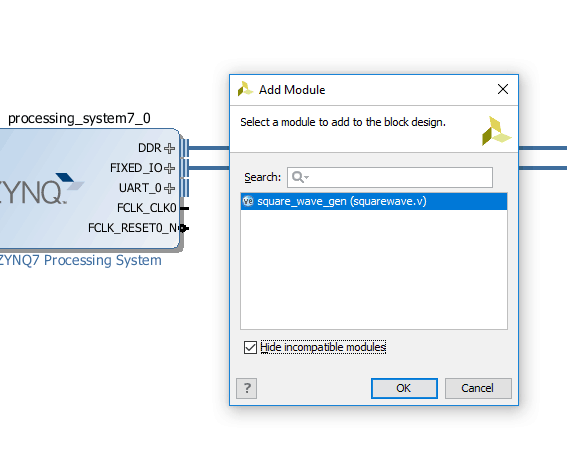
Again right-click in the Diagram Window and select “Add Module…”. Select “square_wave_gen” from the options and click “OK”.
Step 9
Connect Clock and Reset signals from Zynq block to Square Wave Module. Make the sq_wave port as an external port by right-clicking on it and selecting “Make External”. The resultant design should look like this:
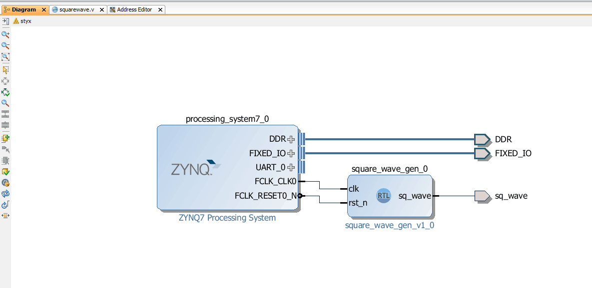
Save the block design.
Step 10
In the sources window, right-click on styx block design file and select “Create HDL Wrapper…”
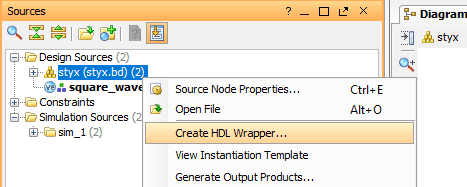
Click OK on the window which pops up.
Step 11
In the sources window, right-click and choose “Edit Constraints Sets…”. Click “Create File” and name it as “styx_sq_wave.xdc”. Then, click OK to let Vivado create the constraint file. In this file, we will add location constraint for `sq_wave` output port which we had created.
Open the “styx_sq_wave.xdc” file and copy below contents into it. Finally, save the constraints file.
set_property -dict {PACKAGE_PIN J22 IOSTANDARD LVCMOS33} [get_ports sq_wave]
We have used first available GPIO on header P4 on Styx as 1Hz square wave output signal.
Step 12
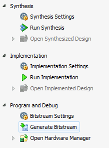
Click “Generate Bitstream” and click “Yes” in any subsequent dialog windows that may pop up.
Step 13
Once bitstream generation is successfully completed, one would normally expect to be able to program the FPGA on Zynq right away to get his/her RTL design working. This would have been true if the design wasn’t using any Zynq PS specific functionality. But, in our case, we are sourcing clock from Zynq PS section. For this to work, we need to first configure the correct registers on Zynq to set up clocking infrastructure for 100MHz output on FCLK_CLK0.
To do this, we need to use Xilinx SDK which ships with Vivado Suite. Go to File -> Export -> Export Hardware... Check “Include bitstream” and click OK.
Now, go to File -> Launch SDK. Click OK in the dialog window which pops up.
Step 14
Put your Styx in JTAG Boot Mode and connect USB cable as well as Xilinx Platform USB Cable II JTAG and power up. In the SDK window, go to File -> Application Project. Type any project name and click Next. Choose “Empty Application” from the Available Templates list, and click Finish. SDK will generate an empty application project, along with a bsp project required for the application project.
Step 15
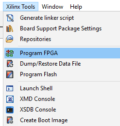
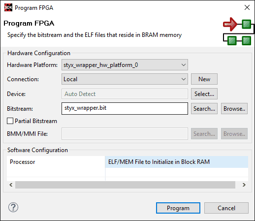
Now we need to program the bitstream first. Then we will initialize the Zynq SoC. Go to Xilinx Tools -> Program FPGA and click “Program” in the Program FPGA window.
Step 16
After FPGA is successfully programmed with the bitstream, we need to initialize the processor. For initializing the processor, we simply run the empty application on the ARM processor of the Zynq SoC. SDK will automatically run the ps7_init.tcl initialization TCL script before running the empty application.
So, right-click on the empty application project, go to Run As -> Launch on Hardware (System Debugger) or Launch on Hardware (GDB).
Step 17
Once the program is launched on hardware, we should now get a 1Hz square wave on the GPIO pin 5 (J22) of Styx GPIO Header P4. Go ahead confirm this with an oscilloscope, or logic analyzer, or even a simple multimeter!
That’s it! We are now using the 100MHz clock sourced from SoC PLL for our RTL designs!
Thank you very much for this tutorial. You’ve taught me in 20 minutes what 3 days of searching and reading couldn’t. Hope the following does help others, who the same as me, are in the pursuit of knowledge.
I’ve been kept from doing real work on my Zynq-7000 (Z-Turn 7z020) board (writing VHDL and only use the Linux part to avoid JTAG), because i couldn’t get any clock signal, which i needed for a simple RGB LED Hello World test.
Also to avoid using JTAG (don’t want to buy another one-use-only cable) and SDK you could use the created BIN file from the “Generate Bitstream” step in Vivado and just copy it via SSH to the running Linux (for me it’s Ubuntu 12.04) on the Zynq Board. A simple “cat filename.bin > /dev/xdevcfg” will do the programming for you.
This is just volatile programming and therefore not lasting, which is exactly what one wants, when in rapid prototyping mode, or if the board is left at home, while one does access it from outside.
February 4, 2018 at 12:47 amGlad you found it useful!
February 12, 2018 at 11:20 amHello,
I step 7 do I need Board Support File form Numatolab. How can I get these files? Is that come with the board. I get the board but don’t get the files. I couldn’t get step 8 at all.
August 23, 2018 at 11:28 pmHi, please get the bsp from here: https://github.com/numato/samplecode/tree/master/FPGA/numatoVivadoBSP
August 29, 2018 at 9:46 amThank you very much. I got to this point myself (beginner and it took me 3 days, would have been easier if I found this blog on day 1 🙂
But the simulation only works in behavioral. There does not appear to be a clock in the post-synth or post-impl simulations?
You would not happen to know how to fix this?
October 17, 2018 at 10:47 amThank you very much for your article. It helped me a great deal with my first launch of Z-turn board. I have a couple of questions, though. Would you be so kind to clarify, is it possible to use free pin Zynq for clock PL (without PS)? As far as I know, in Zybo board there is L16 pin on which the clk can be supplied to the operation of PL. It would be much more convenient to connect external Clock generator (f.ex. MC STM32), instead of working every time with Zynq PS settings for clock PL. Besides, even though this project for FPGA is simple, Zynq heats up (to 55 degrees Celsius) while working.
February 19, 2019 at 6:07 pmThank you for your assistance!
Yes indeed it is possible.
February 25, 2019 at 4:21 amThanks for lucid explaination.
July 31, 2019 at 1:50 pmI followed you until second-last step: Run As -> Launch on Hardware (System Debugger).
Here I get error mentioning “Done pin is not high on target FPGA. Do you want to continue?”
whatever i choose then, i dont get output. please suggest what could have gone wrong. everything worked ok until here without a glitch.
clearly my FPGA is not getting programmed as the green LED is remaining in ON state. It should be OFF after programming, right?
July 31, 2019 at 1:52 pmSorry.
July 31, 2019 at 1:56 pmIt’s launched now.
Actually, First I run but it couldn’t complete and got hang at 99%. In later iteration I forgot to program FPGA first before running *.elf.
100 Mhz though has yet to be seen 😉
thanks, it worked well !
July 31, 2019 at 2:01 pmThank you for the tutorial!
November 10, 2019 at 3:26 amI just wanted to add few things that I lacked in the tutorial (maybe it will be helpful for others):
1. In Sources -> Design Sources, right-click on the PS wrapper and set is as Top Level
2. The names of the pins in constraints file MUST much the ones in the Design Block