Introduction
USB 3.0 (later renamed as USB 3.1 Gen 1) is also known as SuperSpeed USB. It has revolutionized the world of desktops and mobile devices by bringing much higher bandwidth and better power delivery compared to its predecessor USB 2.0. USB 3.1 offers a data rate of 5Gb/s or a whopping theoretical bandwidth of 625MB/s. This is more than 10 times the theoretical maximum bandwidth of USB 2.0. While practically, the available bandwidth for end-user applications can be lower depending on the hardware and firmware solutions chosen, USB 3.1 offers a great value proposition that cannot be ignored. By using these USB 3.1 features Numato Lab has selected USB 3.1 as the host interface for several of their FPGA products. So, in this article, we will show you the USB 3.1 Gen 1 Interfacing with Host System using Callisto Kintex 7 USB 3.1 FPGA Module.
Tools and Prerequisites
Hardware
- Callisto Kintex 7 USB 3.1 FPGA Module
- Xilinx Platform Cable USB II.
- USB A to USB Type C cable
Software
- FT_Prog tool for configuring on-board FT2232H USB Serial converter (download and install from FTDI website).
- Xilinx Vivado Design Suite 2023.2.1
- Python 3.5 or higher
- LiteX
- MinGW
FIFO Master Interface with FT600/FT601
The FT600/FT601 chip is a bridge for USB to the FIFO interface. This FT600/FT601 chip supports USB 3.1 SuperSpeed (5Gbps)/USB 2.0 High Speed (480Mbps)/USB 2.0 Full Speed (12Mbps) transfer. FT600 and FT601 are completely compatible with the USB 3.1 Gen 1 specifications. FT600Q has a 16-bit FIFO bus interface and FT601Q has a 32-bit FIFO bus interface. This Ft600/FT601 supports the two bus protocols, one is the “Multi-Channel FIFO” bus protocol and the other is the “245 Synchronous FIFO” bus protocol. This article uses the “245 Synchronous FIFO” bus protocol to interface with the Host System. Here, FT600/FT601 acts as a slave and FPGA will be the FIFO Master. By connecting the FT600/FT601 chip with Xilinx FPGA we can transfer/receive the data to/from the host system.
Implementation of FIFO Master Interface with FT600/FT601
In this article, the implementation of the USB3.1 Interfacing with Host System is implemented using LiteX and Migen. The below code is the complete implementation of the FIFO Master Interface in Migen.
class FT601_245(Module):

def __init__(self, io, width=32):
# Shared control
# Data bus is driven by both the FPGA and the FTDI. We use tristate.
io.oe_n.reset = 1
io.rd_n.reset = 1
io.wr_n.reset = 1

self.data_tri = data_tri = TSTriple(width)
data_tri.oe.reset = 1
assert io.data.nbits == width
self.specials += data_tri.get_tristate(io.data)

self.be_tri = be_tri = TSTriple(width // 8)
be_tri.oe.reset = 1
assert io.be.nbits == width // 8
self.specials += be_tri.get_tristate(io.be)

self.comb += [
be_tri.o.eq(0xf),
be_tri.oe.eq(1),
data_tri.oe.eq(1),
io.oe_n.eq(1)
]

txe_n_d4 = self.txe_n_d4 = Signal()
txe_n_d5 = self.txe_n_d5 = Signal()
wr_n_d1 = self.wr_n_d1 = Signal(reset=1)
wr_n_d0 = self.wr_n_d0 = Signal(reset=1)
data_d0 = self.data_d0 = Signal(width, reset=0)
data_d1 = self.data_d1 = Signal(width, reset=0)
self.specials += MultiReg(io.txe_n, txe_n_d4, n=txe_delay, reset=1)

self.comb += [
io.wr_n.eq(wr_n_d1),
data_tri.o.eq(data_d1),
]

prefetch_counter = Signal(4, reset=0)
counter = self.counter = Signal(width, reset=0)
self.sync += [
txe_n_d5.eq(txe_n_d4),
data_d1.eq(data_d0),
wr_n_d1.eq(wr_n_d0),

data_d0.eq(counter),
If((txe_n_d4 == 0) & (txe_n_d5 == 0),
wr_n_d0.eq(0),
If(prefetch_counter < txe_delay + 2,
prefetch_counter.eq(prefetch_counter + 1)
).Else(
prefetch_counter.eq(prefetch_counter)
),
counter.eq(counter + 1)
).Elif(txe_n_d4 == 1,
wr_n_d0.eq(1),
prefetch_counter.eq(0),
counter.eq(counter - prefetch_counter)
)
]

class MultiRegImpl(Module):
def __init__(self, i, o, odomain, n, reset=0):
self.i = i
self.o = o
self.odomain = odomain

w, signed = value_bits_sign(self.i)
self.regs = [Signal((w, signed), reset=reset, reset_less=True)
for i in range(n)]

###

sd = getattr(self.sync, self.odomain)
src = self.i
for reg in self.regs:
sd += reg.eq(src)
src = reg
self.comb += self.o.eq(src)
for reg in self.regs:
reg.attr.add("no_retiming")


class MultiReg(Special):
def __init__(self, i, o, odomain="sys", n=2, reset=0):
Special.__init__(self)
self.i = wrap(i)
self.o = wrap(o)
self.odomain = odomain
self.n = n
self.reset = reset

def iter_expressions(self):
yield self, "i", SPECIAL_INPUT
yield self, "o", SPECIAL_OUTPUT

def rename_clock_domain(self, old, new):
Special.rename_clock_domain(self, old, new)
if self.odomain == old:
self.odomain = new

def list_clock_domains(self):
r = Special.list_clock_domains(self)
r.add(self.odomain)
return r

@staticmethod
def lower(dr):
return MultiRegImpl(dr.i, dr.o, dr.odomain, dr.n, dr.reset)

class FT601SourceTop(Module):
def __init__(self, platform):
usb_fifo = platform.request("usb_fifo")

crg = CRG(platform.request(platform.default_clk_name))
self.submodules.crg = crg

usb_phy = FT601_245(usb_fifo)
self.submodules.usb_phy = usb_phy
The following code specifies the pin constraints that are required for the design. All these FPGA pins are connected to the corresponding FT601 pinouts and the communication between FPGA and FT601 will happen through these pins once the above logic is configured to FPGA. Make sure that all the pin constraints are correct for Callisto K7 before generating the bitstream files.
_io = [
    ("clk100",  0, Pins("N21"), IOStandard("LVCMOS25")),

    ("usb_fifo", 0,
        Subsignal("data", Pins("N17 N18 M19 M20 N19 K25 K26 L24 L25 M24 M25 M26 N22 N24 N26 P16 R16 U16 R17 T17 U17 R18 P26 P25 P24 R26 R25 R23 T25 T24 R22 T22")),
        Subsignal("be", Pins("P18 P19 T18 T19")),
        #Subsignal("clk", Pins("Y23")),  # Used as main system clock clk100
        Subsignal("txe_n", Pins("U19")),
        Subsignal("rxf_n", Pins("R20")),
        Subsignal("wr_n", Pins("R21")),
        Subsignal("rd_n", Pins("P21")),
        Subsignal("oe_n", Pins("T20")),
        Subsignal("wakeup_n", Pins("T23")),
        IOStandard("LVCMOS25"),
    ),
]
The below module will convert the code into Verilog and generate a bitstream for the given FPGA part number using the Vivado toolchain.
class CallistoK7Platform(XilinxPlatform):
default_clk_name = "clk100"
default_clk_period = 10.000

def __init__(self, programmer="xc3sprog"):
self.programmer = programmer
XilinxPlatform.__init__(self, "xc7k160tfbg676-2", _io, [], toolchain="vivado")

def create_programmer(self):
if self.programmer == "xc3sprog":
return XC3SProg("jtaghs1")
else:
raise ValueError("{} programmer is not supported".format(self.programmer))


default_subtarget = FT601SourceTop
default_platform = Callisto7Platform

if __name__ == '__main__':
p = CallistoK7Platform()
m = FT601SourceTop(p)
# out = verilog.convert(m, ios=set()))# m.get_ios()))
p.build(m, build_name="ft601_callisto_k7_160t", build_dir="build_callisto_k7_160t")
Interfacing the USB 3.1 Gen 1 with Host System using Callisto K7
Make sure that the LiteX is installed in your system and save the ft601.py file. Open the command prompt to run the following command:
python ft601.py
After running the code, in the directory where the Python file is saved, you will find a folder named “build_callisto_k7_160t”. In this folder, you will get a Bitstream (.bit) file, TCL script, Verilog file, and XDC file.
Now, download the required FTD3XX Host files from here and extract them to any convenient directory on your PC. This d3xx-host folder contains the main.cpp file, FTD3XX library files and other files required to generate the executable file that tests the project.
To generate the executable file, browse to the directory where the d3xx-host folder was extracted and open Command Prompt in that folder and run the following command:
make -f Makefile.mingw32 build
This will create the executable file required to test the project. Now, program Callisto Kintex 7 USB 3.1 FPGA Module with the bitstream (available in “build_callisto_k7_160t” folder) that was generated by running the python file using the Tenagra application (refer the Tenagra article to program the Callisto K7). Once the board is programmed, connect USB type C between Callisto K7 and your PC. Browse to the directory in which the executable file is present and open Command Prompt and run the executable file.
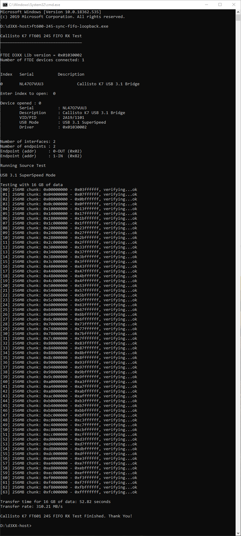
After running the executable file, the FT601 device detects and the FT601 device will read the 16GB of data from the Host device as shown in the image below.
Congratulations! You have successfully interfaced USB 3.1 Gen 1 with the host system using Callisto Kintex 7 USB 3.1 FPGA Module.