For many of us, learning FPGA was a natural next step from the world of micro-controllers and Embedded System. You learn the basics of Embedded System, do some projects using micro-controllers and microprocessors and one day realize that those devices may not be the best choice for a particular problem that you want to solve. A little research could lead you to FPGAs. But the FPGA world is very different from the micro-controller world you have seen so far. While micro-controller and Embedded System experience is very helpful, it can not help you get started with FPGAs without a somewhat steep learning curve. The tools are different, languages are different and even the programming paradigm is different.
But there is hope. By definition (in loose terms) FPGA is a bunch of logic elements that can be configured to make any logical circuit. If that is true, why not make a microprocessor out of those logic cells and program using traditional Embedded System friendly languages and tools? Yes, it is possible. But there is a question as to why this method of making a microprocessor or micro-controller out of FPGA logic is better compared to off the shelf microprocessors? There are many reasons why making microprocessor/controller in FPGA fabric is better (or worse) compared to an off-the-shelf micro. The most important reason is that you have access to the FPGA fabric from the micro-controller (through buses and peripherals created within the fabric, of course) and you can implement peripherals from a vast array of Xilinx’s freely available peripheral IPs or create your IP (or buy third-party IPs). It is possible to make pretty much any peripheral that you want within the capability of the FPGA that you have chosen to work with. There are a few important downsides to this scheme though. The total cost of hardware will be usually higher compared to an off-the-shelf micro for the same amount of raw processing power. If you can not find the peripheral IP that you are looking for, you will end up having to write one using Verilog or VHDL and you are back to square one (remember, what we wanted to do was not to deal with HDLs or FPGA workflow at all). It is possible to buy third-party IPs but depending on the specific IP, it can be very expensive. Also, it is worth mentioning that the tools required to build an embedded system out of FPGA could set you back by a few hundred dollars.
Let us take a look at what a processor-based embedded system built into an FPGA would look like in it’s simplest form. As you can see in the diagram below, an embedded system built in FPGA fabric is not really different from any other embedded system. It has a processor, memory, buses, and peripherals etc. everything that you would expect in a normal Embedded System configuration. It is just that the processor, buses, and peripherals are all made by using logic cells that are available within the FPGA.
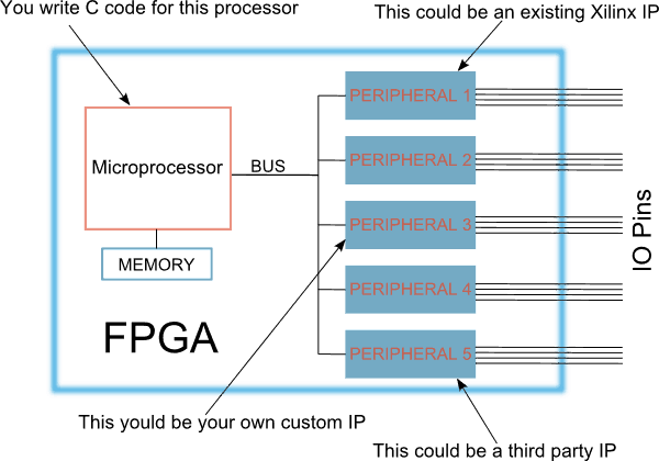
As you can see here, you could use a variety of peripherals from a variety of sources. The peripherals could be communication peripherals such as I2C, SPI, UART or signal processing cores such as FFT, filters or anything that you could imagine and implement on the FPGA fabric. This flexibility gives FPGA based embedded systems an edge in some situations compared to traditional microcontrollers where peripheral choices are often less flexible.
Embedded Infrastructure by Xilinx
Xilinx is arguably the world leader in FPGA and other programmable logic. They provide tools for building embedded systems around many of their FPGAs. Xilinx offers two kinds of fundamental options when it comes to implementing an Embedded system.
- Processor instantiated on FPGA fabric or so-called Soft Processors (Microblaze, Picoblaze)
- Hard processor on the die which has dedicated connectivity to FPGA fabric
As you can imagine, soft processors will use part of FPGA fabric to function and you have to be happy with what is left in order to implement your own peripherals. But with Hard processor cores, FPGA fabric is not used for implementing the processor and you will have 100% of FPGA fabric (or close to 100%) to implement your own peripherals. Hard processor cores are usually more powerful as well. But as of writing this article, the price of FPGAs with built-in hard processor cores tend to be higher.
During this tutorial we will stick with Soft processors, Microblaze to be specific. This is because Microblaze can be implemented on relatively inexpensive hardware such as Mimas A7. Please note that Microblaze soft processor is not compatible with Spartan 3 devices.
In simple terms developing an Embedded System with Xilinx FPGAs consists of the following steps.
- Create a Microblaze based embedded system project
- Add additional peripherals as necessary
- Configure the processor and other subsystems
- Build the processor core and all subsystems to generate a bit file that can be programmed to FPGA
- Create a software project that can run on the hardware infrastructure already made
- Write your own program in C and build
- Download everything to the FPGA and run
While it sounds a little complicated, Xilinx’s powerful tools make it very easy to implement those steps in practice. In fact, we will implement a working Embedded System with writing less than 10 lines of code. Now it looks like it is the right time to introduce Xilinx’s tools that we will use to accomplish the above steps. We will be using the following tools throughout the rest of this tutorial.
- Xilinx Vivado Design Suite 2018.2 (https://www.xilinx.com/support/download.html)
- Xilinx SDK
Xilinx Vivado Design Suite is the tool you will use to design the hardware part of the embedded system (Processor, peripherals, buses etc..). Xilinx SDK is a software development environment based on Eclipse IDE. A lot of people will find the SDK tool visually very familiar because of this. Using SDK, you can create software projects and write C code that would run on the Embedded System designed using Vivado. Confused? don’t worry, everything will become much clearer when we go through the process step by step.
Xilinx Vivado and SDK can be downloaded and installed from Xilinx website as a single package. But they are licensed separately. You will need one license for Vivado (unlimited license but device limited, good enough for these tutorials) and another license for SDK (Can be purchased here. Xilinx used to offer 30-day evaluation license. Please contact Xilinx to find out more information). How to download, install and license these tools is beyond the scope of this tutorial. Please visit xilinx.com to get more help on this.
Let’s get our hands dirty
To keep this tutorial concise and easy to follow, we will implement a simple Hello World Embedded System. Once implemented, it will print “Hello World” through the serial port. We will use the Mimas A7 FPGA Development Board as the hardware platform to implement this project. Mimas A7 has an Artix 7 7A50T FPGA and an onboard USB – Serial converter which would help us print data to the PC.
Configuring and Building Microblaze Soft Processor and Peripherals
So far we have looked at some basics and selected a hardware platform. Now we will create a project using Xilinx Vivado Design Suite and configure Microblaze based soft processor and some peripherals. Before we can create a project we must copy some supporting files to the vivado installation directory. These files will help us create and configure the project with a few simple mouse clicks. Download the vivado BSP files for Mimas A7 and extract the contents to the “board_files” directory within Xilinx Vivado installation. If you have installed Vivado 2018.2 on C:\ drive, the whole path to these files will be C:\Xilinx\Vivado\2018.2\data\boards\board_files
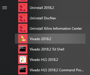
Now launch Xilinx Vivado Design Suite 2018.2 from the start menu.
Step 1:
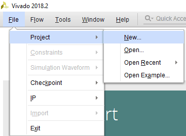
Start Vivado Design Suite, and create a new project from “File–> Project–> New”. The “New Project” wizard will pop up. Press “Next” on window to proceed with creating the project.
Step 2:
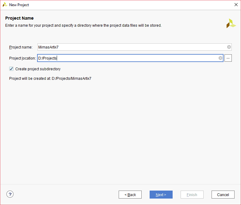
Type in a name for the project and save it in a preferred location. This examples calls the project “MimasArtix7” but feel free to use any name. Select the check box below to keep all project files in a single folder. The image below shows the settings for the example project. Click “Next” to continue.
Step 3:
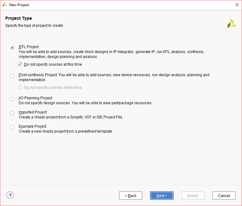
At the “Project Type” tab, select “RTL Project” and check “Do not specify sources at this time”. Click “Next” to proceed.
Step 4:
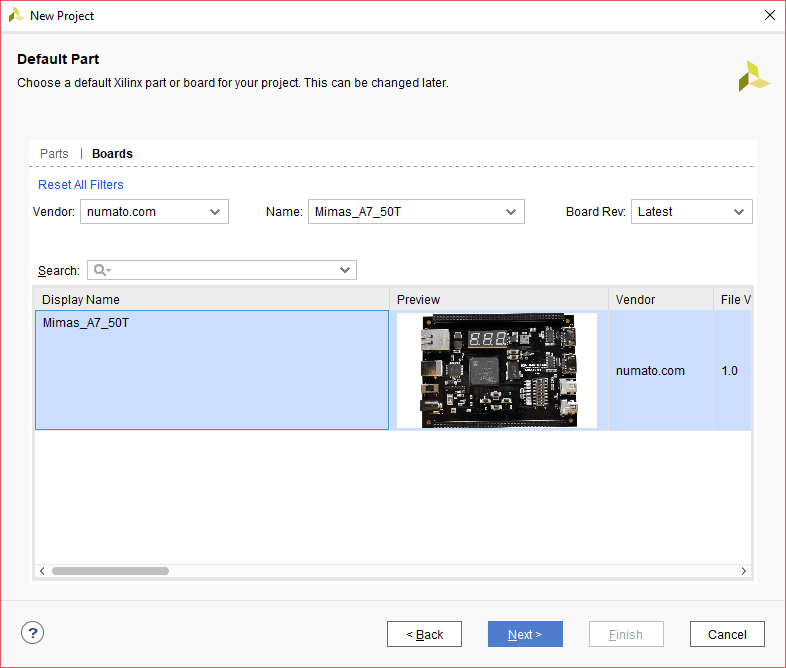
At the “Default Part” step, select “Boards” and then select “Mimas_A7_50T” and then click “Next”. If Mimas_A7_50T is not displayed in the boards list, you will need to install Mimas A7 board support files appropriately and retry this step. You can download Mimas A7 support files for Vivado from here.
Step 5:
Click “Next”. In the next window, check the summary and then click “Finish”.
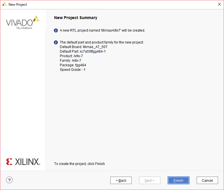
When the new project wizard exits, a new project will be opened up in Vivado with the settings you have selected with the wizard.
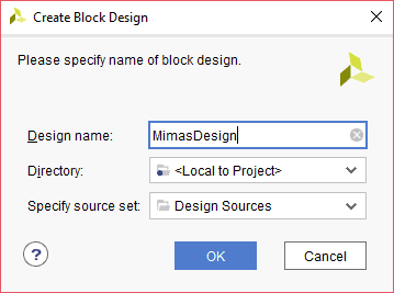
Step 6:
In the Flow Navigator panel, select “Create Block Design” under the “IP INTEGRATOR”. Give an appropriate name to design. We will call it as “MimasDesign” in this article.
Step 7:
Select the “Board” tab, the default peripherals available for the selected board (Mimas A7 FPGA Module in our case) will be displayed.
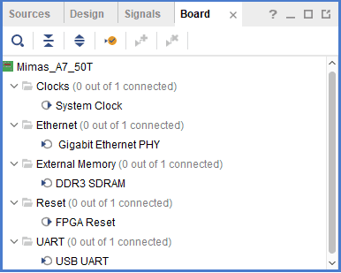
Step 8:
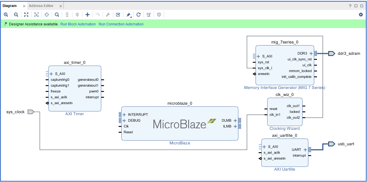
Add System Clock, USB UART and DDR3 SDRAM to the design by double clicking on the corresponding peripherals listed. Then go to Diagram window, right click and select “Add IP” from the popup menu.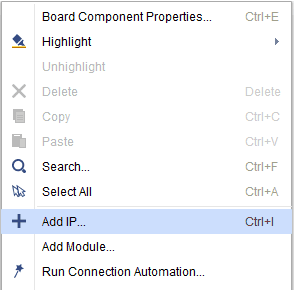
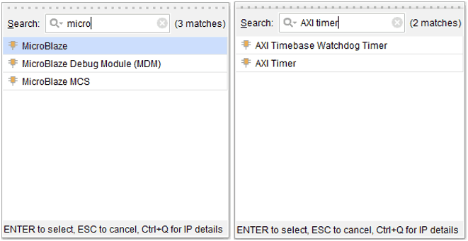
Search for Microblaze and AXI Timer IPs and add them to design by double clicking on them.
Step 9:
Double click on “Clocking Wizard” IP and configure it with the settings as shown below.
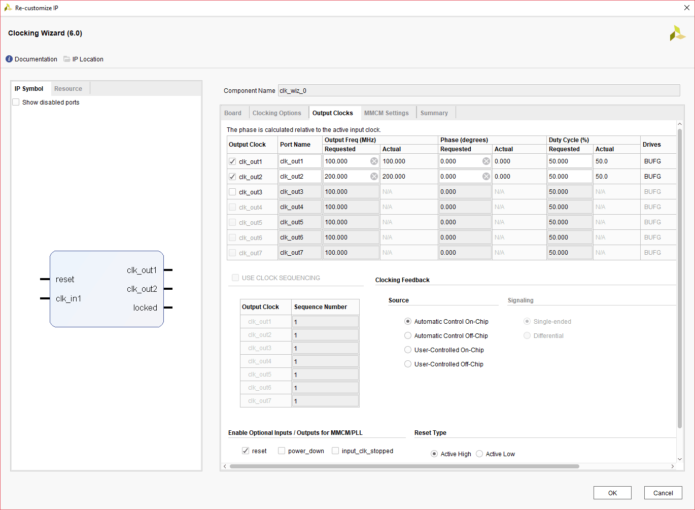
Step 10:
Remove the sys_clk_i existing connection from MIG IP and connect it to clk_out2 net on the “clocking Wizard” as shown in the image below.
Step 11:
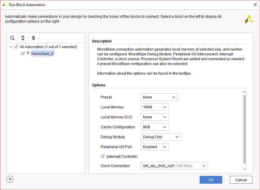
Click “Run Block Automation” on the top left corner of the window to complete the design. Select the settings as shown below. Click “OK” then the blocks automatically configure for you. Once Block Automation is complete, run “Connection Automation” so Vivado can connect the blocks together to make a complete system.
Step 12:
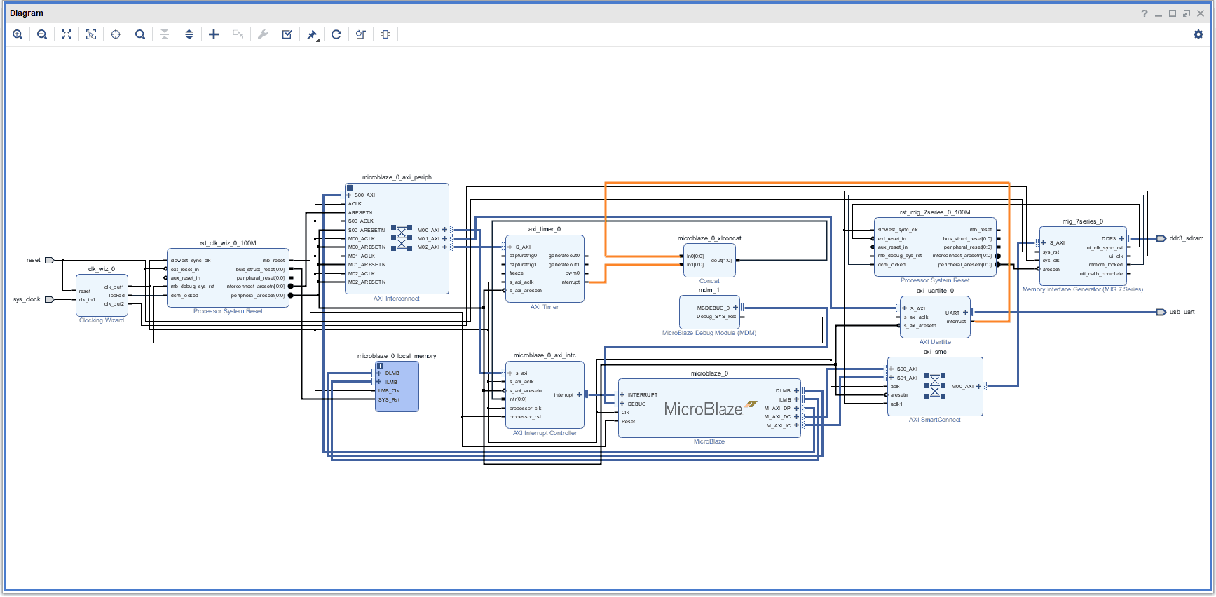
Connect interrupt signals from “AXI Timer” and “AXI UARTLite” to the Concat block as shown in the below image. The lines in question are highlighted in orange.
Step 13:
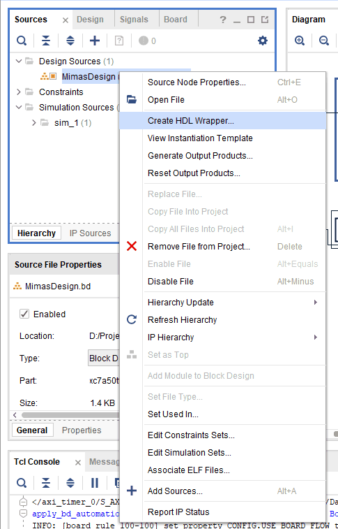
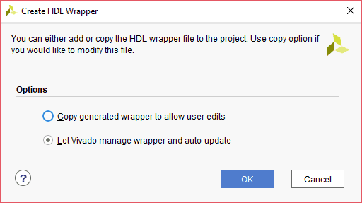
Right click on the design in the Sources -> Design Sources tab, and select “Create HDL Wrapper” from the popup menu. Click OK on the window that appears to finish generating wrapper.
Step 14:
Now double click on “Generate Bitstream” under the Flow Navigator -> PROGRAM AND DEBUG. Wait for the bitstream to complete.
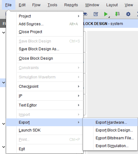
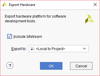
Step 15:
Once the bitstream is generated successfully, we need to export the hardware along with the bitstream. From File menu, select Export -> Export Hardware.
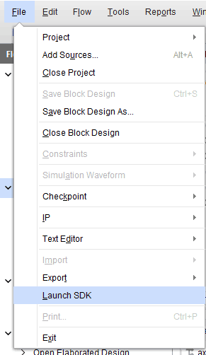
Step 16:
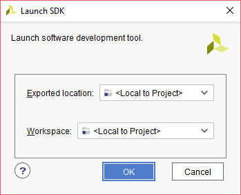
Launch SDK from File menu. Click “Ok”.
Step 17:
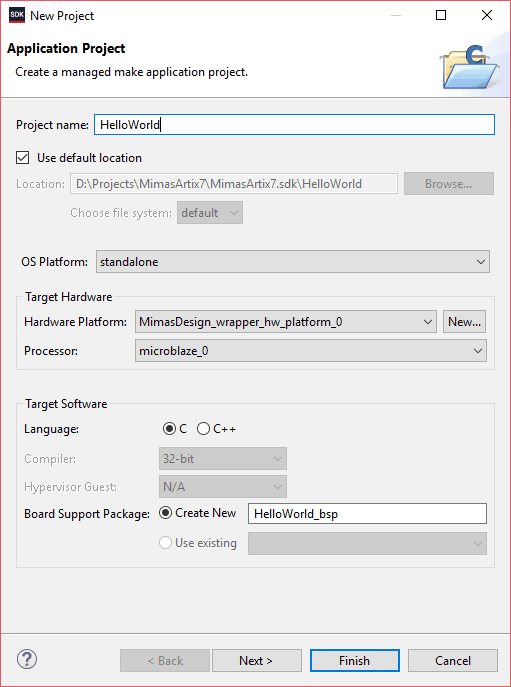
Once SDK window appears, select “Application Project” from File menu -> New. Type in a Project name (The author used “HelloWorld” as project name in this article). Click “Next”.
Step 18:
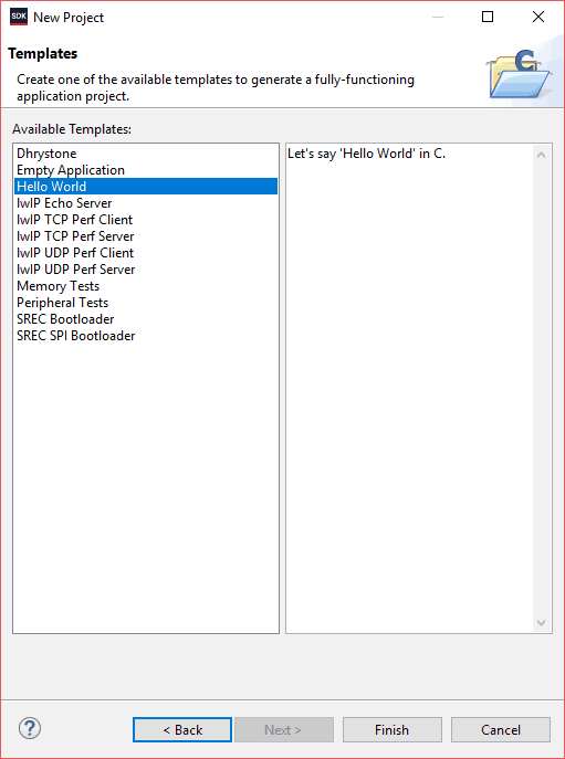
Now select “Hello World” template from the list of available templates and click “Finish”.
Step 19:
Once the project is created, SDK will automatically run a build. If that didn’t happen for any reason, run a build manually. Once the build is completed successfully, power up Mimas A7 FPGA Module and connect Xilinx Platform USB cable and USB Type B cable for Serial debugging to the board.
Step 20:
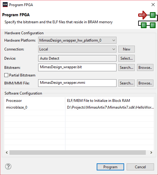
Program the board by selecting “Program FPGA” under “Xilinx Tools/Xilinx” menu. Open the serial port corresponding to Mimas A7 on your operating system using your preferred Serial Terminal software such as HyperTerminal, PuTTY, Tera Term etc..
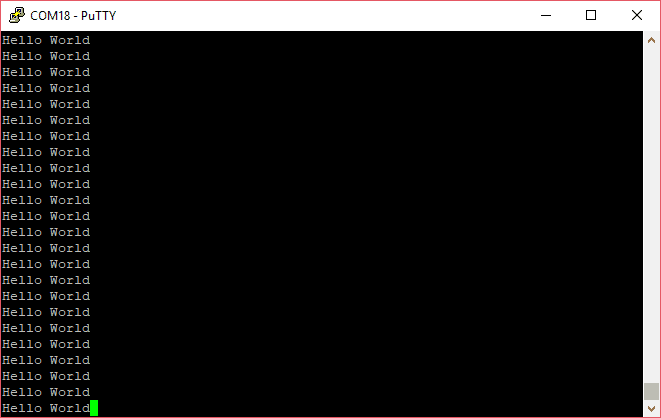
Open any serial terminal and connect to the COM Port corresponding to Mimas A7 board. If everything went well, the application running on the board should print “Hello World” continuously over the USB UART and should be displayed on the Serial Terminal application.