Introduction:
HDMI (High-Definition Multimedia Interface) can be viewed as a digital upgrade of VGA standard. It supports high resolution displays as well as audio data embedded along with video. The pixel data is serially transferred at ten times of pixel clock frequency using TMDS (Transition Minimized Differential Signalling) to minimize the transitions between 1s and 0s. This article actually demonstrates DVI-D output using Styx Xilinx Zynq FPGA Module. DVI-D is a subset of HDMI and has same electrical and physical layer implementation as HDMI. So, all HDMI monitors should be capable of receiving the DVI-D signals transported over HDMI cable.
Prerequisites:
Hardware:
- Styx Xilinx Zynq FPGA Module
- Saturn IO Breakout Module
- HDMI Expansion Module
- Xilinx Platform Cable USB II (optional)
- HDMI cable and a compatible monitor
Software:
- Vivado (version 2017.3 or higher)
Step 1:
Download and install Vivado Board Support Package files for Styx from here. Follow the README.md file on how to install Vivado Board Support Package files for Numato Lab boards.
Step 2:
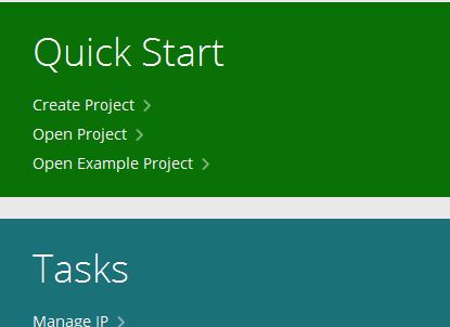
Open Vivado and select ‘Create Project’ in the “Quick Start” area. Click ‘Next’ in the “New Project” dialog window which opens.
Step 3:
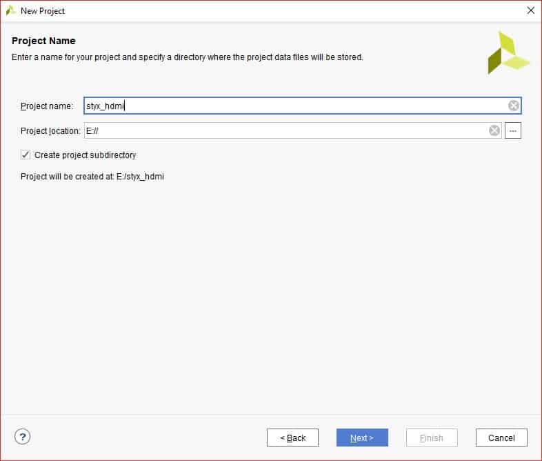
In Project Name page, provide project name of your choice and choose the directory where you want to save the project.
Step 4:
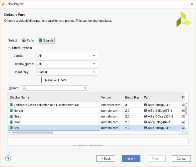
Click Next without making any changes till you see the ‘Default Part’ tab and select ‘Styx’ from ‘Boards’ option. If Styx is not listed, make sure board support files are installed correctly.
Step 5:
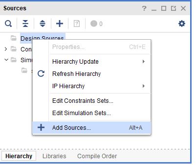
Click Next and Finish to create the project. Then in the Sources tab, right-click Design Sources and click ‘Add Sources’. It will open a new “Add Sources” window.
Step 6:
Download and extract the RTL source files from here and add them to the project by selecting ‘Add Files’.
The HDMI interface has 3 pairs of differential data signals and 1 pair of differential clock signals:
data_p[2:0] & data_n[2:0]: These are HDMI/DVI differential signals carrying the video data to be displayed on screen.clk_p & clk_n: HDMI pixel clock differential pair of signals.
First, VGA signals are generated inside vga module. Then the VGA signals are encoded to 10-bits per channel and the data is then serialised to 10x of pixel clock rate. Finally the three channels along with pixel clock are driven out using TMDS differential drivers.
In the top module (dvid_test), the two submodules dvid and vga are instantiated. Clocking IP (clocking wizard) is used to generate clocks for VGA and DVI-D.
dvid_test: In this module, a “Clocking Wizard” IP core is instantiated to generate required clocks for VGA and DVI-D. A 100MHz clock from the onboard oscillator is provided as input, and following clocks are derived from it:
clk_vga: 25MHz clock. This is the pixel clock frequency for 640×480@60Hz VGA resolution.clk_dvi&clk_dvin: 125 MHz clocks.clk_dvinis 180 degrees out of phase toclk_dvi. These clocks are used for serialization using ODDR2.
vga: VGA signals are generated in this module. This design generates VGA at 640×480@60 Hz resolution.
dvid: VGA signals and clocks are given as input to this module and the DVI TMDS signals are generated as the output. It uses TMDS_encoder module to generate TMDS signals. TMDS uses 8b/10b encoding in which the 8-bit color data (red, green & blue) generated in VGA module is converted to 10 bits. Then this data is serialised using ODDR2 (Double Data Rate primitive). The 10-bit TMDS data is generated at 25 MHz. ODDR2 uses 5 times the frequency of pixel clock (i.e. 125MHz) to serialize the 10-bit encoded data. Note that ODDR2 serialises 2-bits in 1 clock cycle of 125MHz clock. This serialised data is converted into differential signals in top module (dvid_test) using OBUFDS drivers.
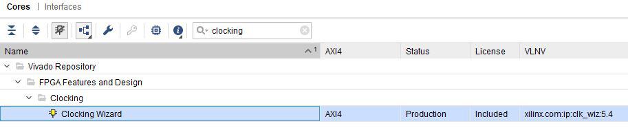
Step 7:
Add Clocking Wizard by clicking on IP catalog in Project Manager, type ‘clocking’ in search box and double-click ‘Clocking Wizard’ IP. It will open customisation window for ‘Clocking Wizard’.
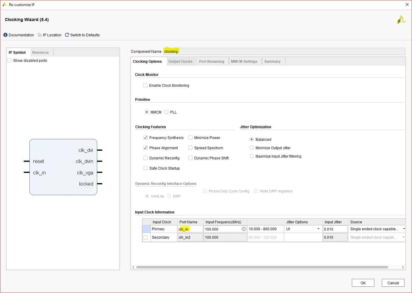
Step 8:
In ‘Clocking Options’ tab, give Component Name as ‘clocking’ and primary clock port name as ‘clk_in’.
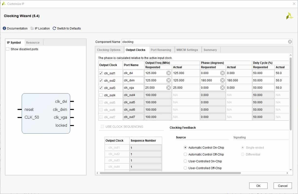
In ‘Output Clocks’ tab, enable 3 output clocks and provide their name, frequency as well as phase as shown in the image below. Click ‘OK’.
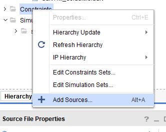
Step 9:
In Sources tab of Vivado, Left-Click ‘Constraints’ and click ‘Add Sources’.
Step 10:
Click ‘Create File’ and enter ‘styx_hdmi’ as File name. Click ‘OK’ and ‘Finish’.
Copy the following constraints to the newly created constraints file:
set_property -dict { PACKAGE_PIN "W16" IOSTANDARD TMDS_33 } [get_ports {clk_p}] ;
set_property -dict { PACKAGE_PIN "Y16" IOSTANDARD TMDS_33 } [get_ports {clk_n}] ;
set_property -dict { PACKAGE_PIN "W15" IOSTANDARD TMDS_33 } [get_ports {data_p[0]}] ;
set_property -dict { PACKAGE_PIN "W17" IOSTANDARD TMDS_33 } [get_ports {data_p[1]}] ;
set_property -dict { PACKAGE_PIN "R20" IOSTANDARD TMDS_33 } [get_ports {data_p[2]}] ;
set_property -dict { PACKAGE_PIN "Y15" IOSTANDARD TMDS_33 } [get_ports {data_n[0]}] ;
set_property -dict { PACKAGE_PIN "W18" IOSTANDARD TMDS_33 } [get_ports {data_n[1]}] ;
set_property -dict { PACKAGE_PIN "R21" IOSTANDARD TMDS_33 } [get_ports {data_n[2]}] ;
set_property IOSTANDARD LVCMOS33 [get_ports {clk_in}] ;
set_property PACKAGE_PIN Y6 [get_ports {clk_in}];
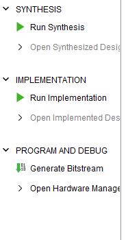
Step 11:
In Project Manager tab, Click ‘Run Synthesis’. If Synthesis is successful, Click ‘Run Implementation’ and finally on successful implementation select ‘Generate Bitstream’.
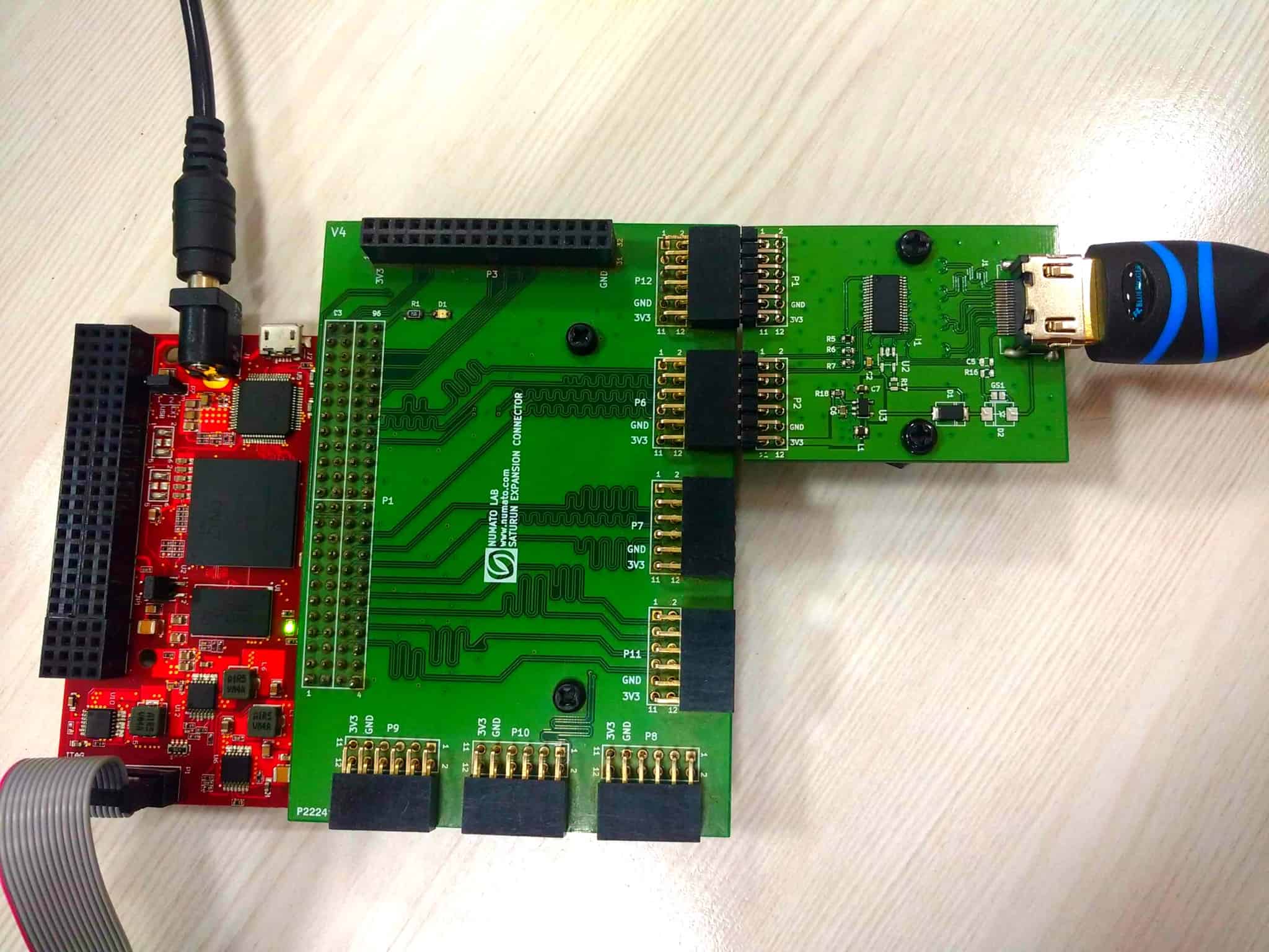
Step 12:
Set up the hardware for testing the design. For this, connect Saturn IO Breakout Module to ‘Header P5’ of Styx. Connect ‘Header P1 & P2’ of HDMI Module to ‘Header P12 & P6’ of Saturn IO Breakout module respectively. HDMI cable between HDMI Expansion module and the monitor. Finally, connect JTAG cable and power supply for Styx.
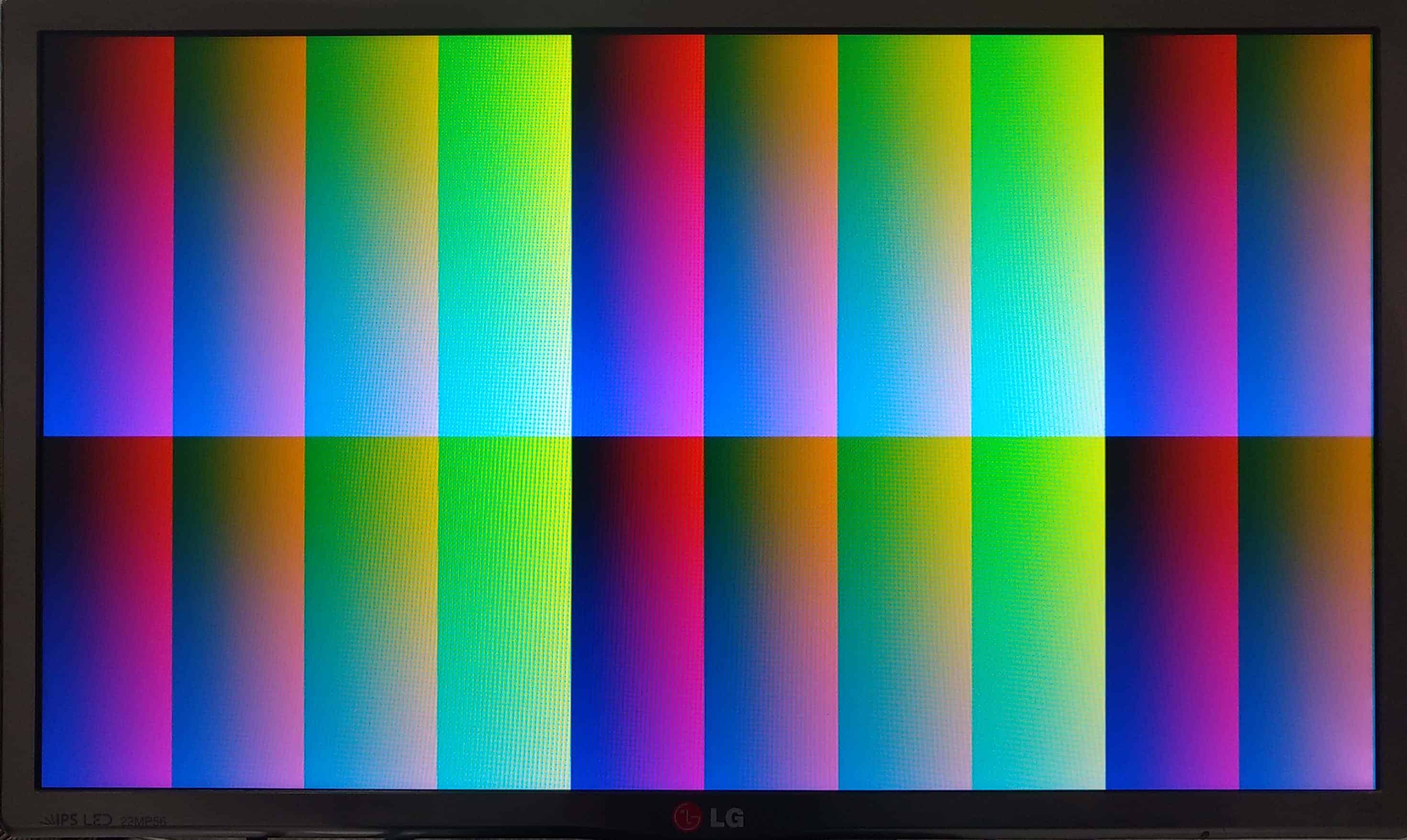
Step 13:
Program the Styx with the generated bitstream. Once Styx is successfully programmed, it should begin generating HDMI signals and the monitor should display a colorful pattern at 640×480 @ 60Hz resolution.
That was it! You can play with the vga module to output different patterns and try to generate higher resolutions as well.