Introduction:
PCI Express is a serial expansion bus standard operating at multi-gigabit data rates. It is the third generation, high-performance I/O bus which is used for interconnecting peripheral devices. PCI Express provides a higher rate of data transfer and lower latency compared to the older PCI and PCI-X technologies which implemented parallel I/O buses. Each device that is connected to the motherboard via PCI Express link has a dedicated point-to-point connection and as it is not sharing the same bus, it doesn’t have to compete for bandwidth. PCI Express is based on the point-to-point topology where dedicated serial links connecting every device to the root complex. This article implements a simple design to demonstrate how to write and read data to HSFPX002 FPGA Module which acts as a PCI Express endpoint device. Let’s get started!
Hardware required:
- Host PC with Linux or Windows (Linux preferred)
- HSFPX002 FPGA Module
- HSFPX00X Carrier Board
- Xilinx Platform Cable USB II (JTAG cable)
- USB A to USB Type C cable
Software required:
- Vivado 2018.2 or newer
- RW-Everything (for Windows host)
Step 1:
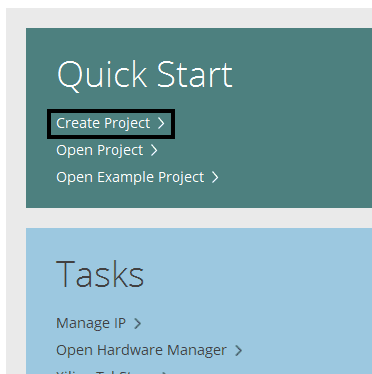
Open Vivado and select “Create Project” from the “Quick Start” section.
Step 2:
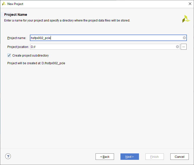
Click “Next” and then in the ‘Project Name’ tab, give an appropriate name and location then check the “Create project subdirectory” box and click “Next” till you see the ‘Default Part’ tab.
Step 3:
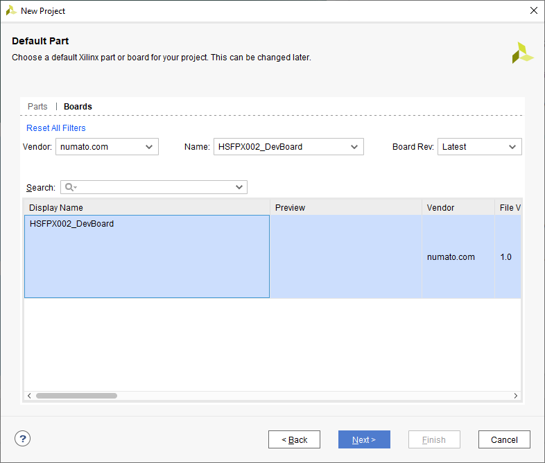
Select “Boards” from the “Default Part” tab, choose “numato.com” as Vendor. Select “HSFPX002_DevBoard” and click “Next”. If HSFPX002 is not listed, make sure the board support files are installed correctly. Click “Finish”. A new Vivado project will open with the selected settings.
Step 4:
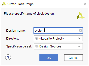
Click “Next” and then “Finish” to create the project. Click “Create Block Diagram” from the IP integrator tab on left, give a name for block design, and click OK.
Step 5:
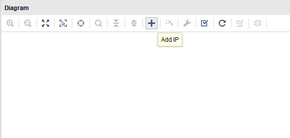
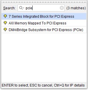
Click “Add IP” from the toolbar as shown in the image below. Type “pcie” in the search box and double click on “7 Series Integrated Block for PCI Express” IP to add it to the design.
Step 6:
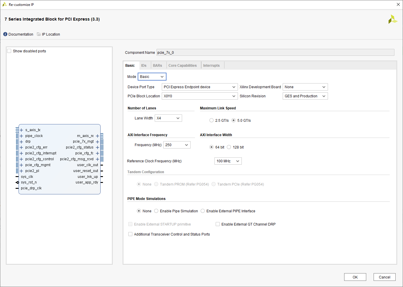
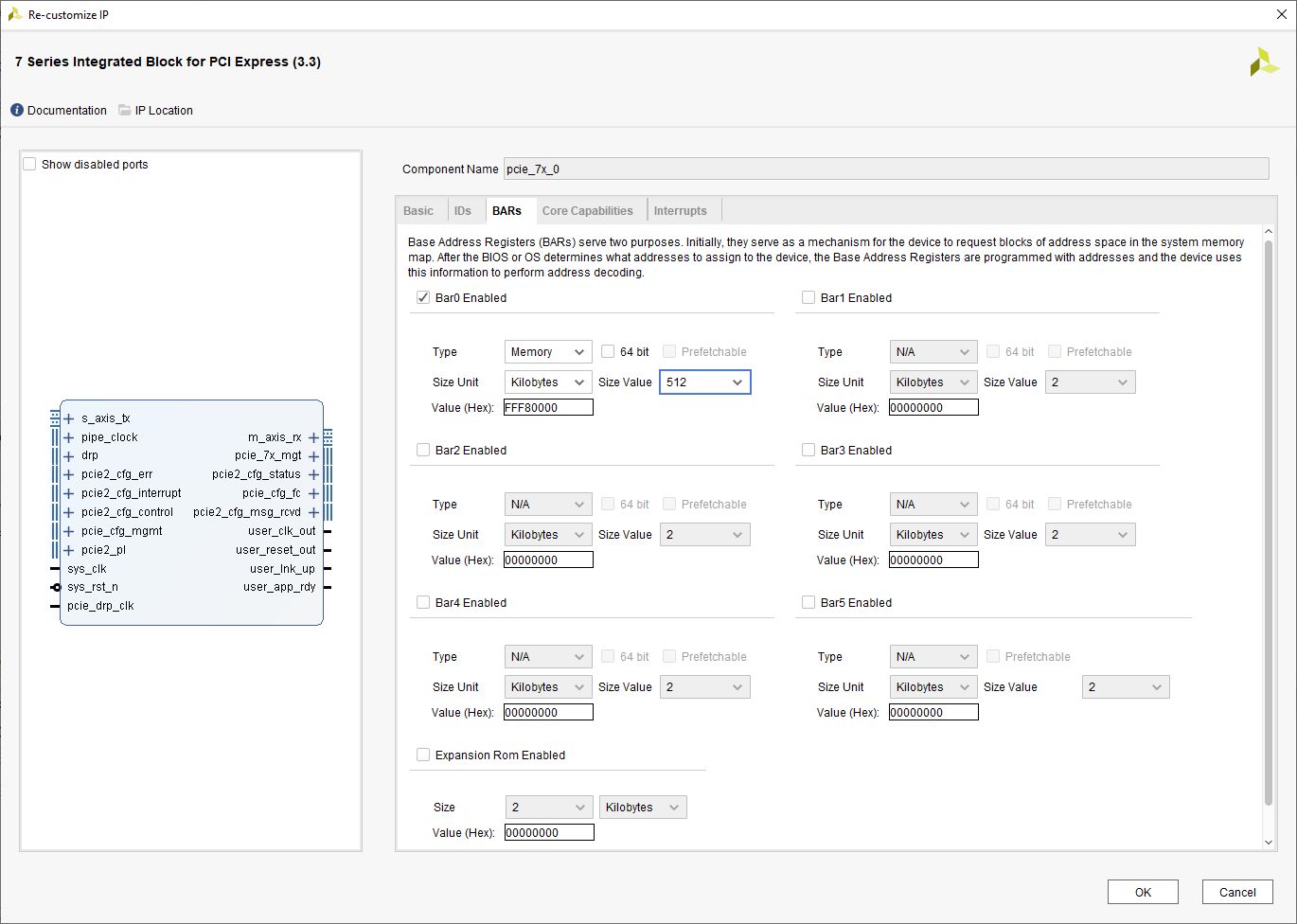
To make the IP compatible with the PCIe specifications of the HSFPX002 board, double click on the “7 Series Integrated Block for PCI Express” IP to customize it. The “Re-customize IP” window should open. In the Basic tab, Select “Lane Width” as “X4”, “Maximum Link Speed” as “5.0 GT/s”. In the “BARs” Tab, select Size Value as “512”. Leave the other tabs in their default state and click OK.
Step 7:
Right-click on the “pcie_7x_0” IP block in the block diagram and click “Open Example IP design…”.
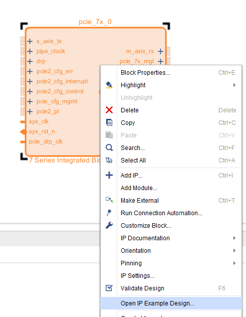
It will open an example project for the PCI Express Endpoint Device as per the customized IP settings. This tutorial uses this generated example project by Xilinx. It already has RTL logic, enabling users to write data to FPGA and read back from it via PCI Express.
Step 8:
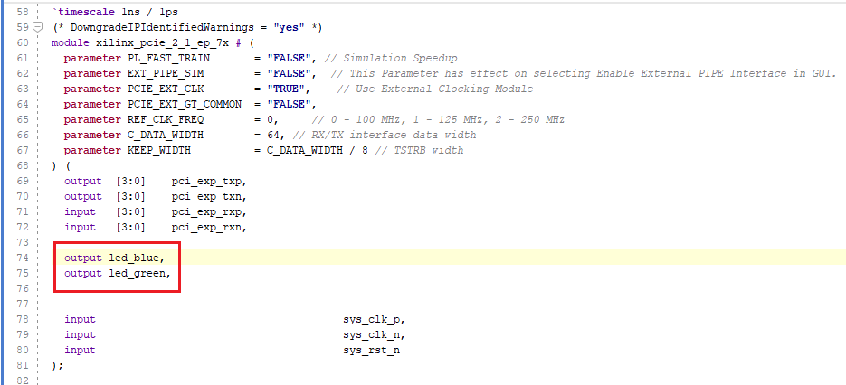
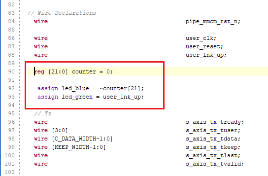
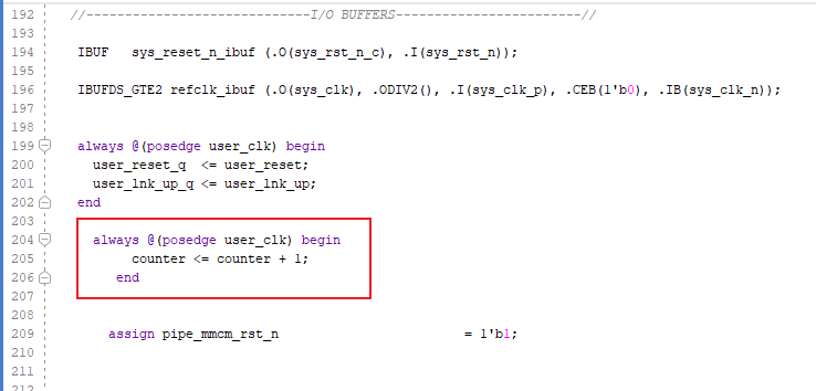
In the pcie_7x_0 IP example design, there is a user_lnk_up logic to indicate that the PCIe link between the host PC and the FPGA is ready to exchange the data when we connect the FPGA board to the PCIe slot of the motherboard. HSFPX002 board features a Bi-Color LED. Hence, connect the user_lnk_up logic output to the Green LED. The Green LED will glow when the PCIe link is ready to exchange the data. So by connecting the user_lnk_up to this LED, we can observe that the PCIe link between the host the PC and the FPGA is ready to exchange the data or not. Also, add the counter to check whether the PCIe clock is working or not, and assign the counter output to the Blue LED. So that we can observe the Bi-Color LED blinking when the board is detected by the host PC.
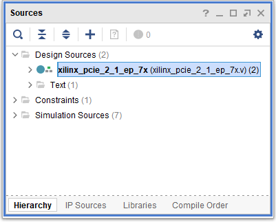
To add this logic, open the Verilog file from the Design Sources category under the Sources tab.
In the Verilog code, in the Ports declarations, add the following:
And under Wire Declarations, add the following:
And then under the I/O Buffers section, add the counter implementation:
Step 9:
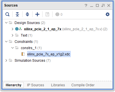
Open the .xdc file from the “Constraints” category under the Sources tab.
Select everything and delete it. Simply copy the following constraints in that file.
set_property IOSTANDARD LVCMOS33 [get_ports sys_rst_n]
set_property LOC T15 [get_ports sys_rst_n]
set_property PULLUP true [get_ports sys_rst_n]

set_property -dict {PACKAGE_PIN B11} [get_ports {pci_exp_rxp[3]}]
set_property -dict {PACKAGE_PIN A11} [get_ports {pci_exp_rxn[3]}]
set_property -dict {PACKAGE_PIN B7} [get_ports {pci_exp_txp[3]}]
set_property -dict {PACKAGE_PIN A7} [get_ports {pci_exp_txn[3]}]

set_property -dict {PACKAGE_PIN D14} [get_ports {pci_exp_rxp[2]}]
set_property -dict {PACKAGE_PIN C14} [get_ports {pci_exp_rxn[2]}]
set_property -dict {PACKAGE_PIN D8} [get_ports {pci_exp_txp[2]}]
set_property -dict {PACKAGE_PIN C8} [get_ports {pci_exp_txn[2]}]

set_property -dict {PACKAGE_PIN B13} [get_ports {pci_exp_rxp[1]}]
set_property -dict {PACKAGE_PIN A13} [get_ports {pci_exp_rxn[1]}]
set_property -dict {PACKAGE_PIN B9} [get_ports {pci_exp_txp[1]}]
set_property -dict {PACKAGE_PIN A9} [get_ports {pci_exp_txn[1]}]

set_property -dict {PACKAGE_PIN D12} [get_ports {pci_exp_rxp[0]}]
set_property -dict {PACKAGE_PIN C12} [get_ports {pci_exp_rxn[0]}]
set_property -dict {PACKAGE_PIN D10} [get_ports {pci_exp_txp[0]}]
set_property -dict {PACKAGE_PIN C10} [get_ports {pci_exp_txn[0]}]


set_property -dict { PACKAGE_PIN "K18" IOSTANDARD LVCMOS33 SLEW FAST} [get_ports { led_green }]
set_property -dict { PACKAGE_PIN "L19" IOSTANDARD LVCMOS33 SLEW FAST} [get_ports { led_blue }]


#set_property LOC IBUFDS_GTE2_X0Y3 [get_cells refclk_ibuf]

###############################################################################
# Timing Constraints
###############################################################################
create_clock -name sys_clk -period 10 [get_ports sys_clk_p]
set_property -dict {PACKAGE_PIN F11} [get_ports {sys_clk_p}]
set_property -dict {PACKAGE_PIN E11} [get_ports {sys_clk_n}]


#
set_false_path -to [get_pins {pcie_7x_0_support_i/pipe_clock_i/pclk_i1_bufgctrl.pclk_i1/S0}]
set_false_path -to [get_pins {pcie_7x_0_support_i/pipe_clock_i/pclk_i1_bufgctrl.pclk_i1/S1}]
#
#
set_case_analysis 1 [get_pins {pcie_7x_0_support_i/pipe_clock_i/pclk_i1_bufgctrl.pclk_i1/S0}]
set_case_analysis 0 [get_pins {pcie_7x_0_support_i/pipe_clock_i/pclk_i1_bufgctrl.pclk_i1/S1}]
set_property DONT_TOUCH true [get_cells -of [get_nets -of [get_pins {pcie_7x_0_support_i/pipe_clock_i/pclk_i1_bufgctrl.pclk_i1/S0}]]]


#
# Timing ignoring the below pins to avoid CDC analysis, but care has been taken in RTL to sync properly to other clock domain.
#
###############################################################################
# Tandem Configuration Constraints n
###############################################################################

set_false_path -from [get_ports sys_rst_n]

###############################################################################
# End
###############################################################################
set_property BITSTREAM.CONFIG.CONFIGRATE 16 [current_design]
set_property BITSTREAM.GENERAL.COMPRESS TRUE [current_design]
set_property BITSTREAM.CONFIG.SPI_BUSWIDTH 4 [current_design]
Step 10:
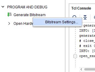
Right-Click “Generate Bitstream” under the “PROGRAM AND DEBUG” section and select “Bitstream Settings”.
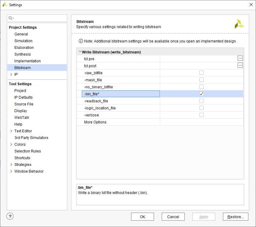
In the “Bitstream Settings” window, select “-bin_file” and click OK.
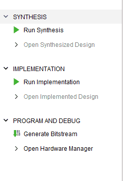
Now, click on “Generate Bitstream” to synthesis, implement and generate the bitstream.
Step 11:
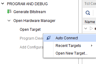
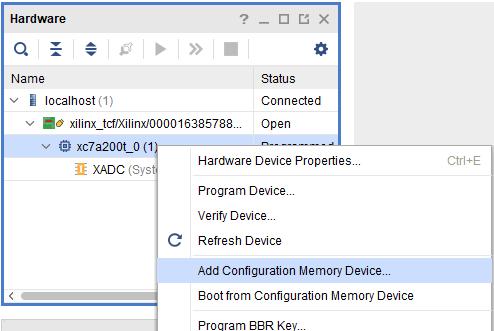
To program the board, open the target by clicking on the “Open Target” in “Open Hardware Manager” in the “Program and Debug” section of the Flow Navigator window. Select “Auto Connect”.
If the device is detected successfully, then select “Add Configuration Memory Device” by right click on the target device “xc7a200t_0” as shown below.
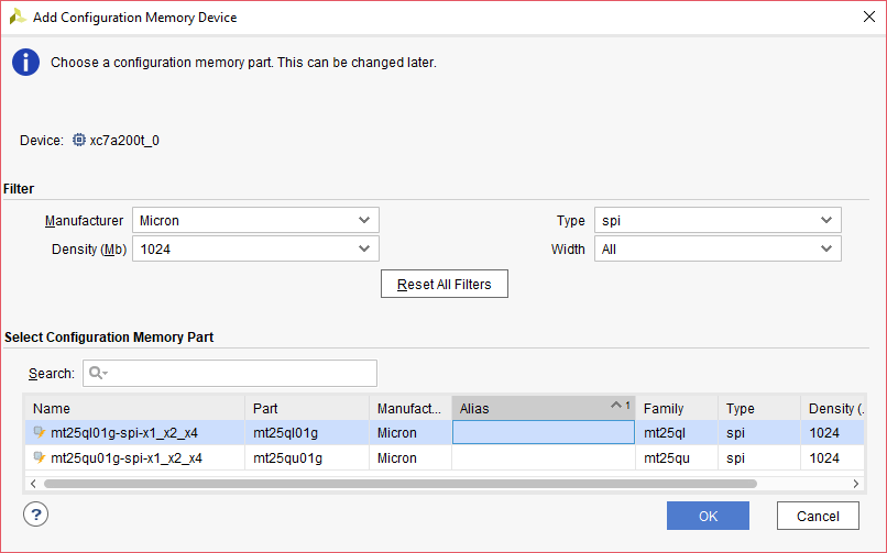
Select the memory device “m25ql01g-spi-x1_x2_x4”, then click OK.
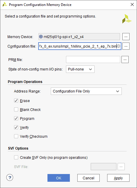
A dialogue window will appear asking if you want to program the configuration device now. Click OK and program the “.bin” bitstream file which is located in “<project location>/ProjectName.runs/impl_1” directory.
Step 12:
Once the device is programmed, test it on a Windows or Linux machine.
Communicating with HSFPX002 via PCI Express on Linux Machines:
Step 1:
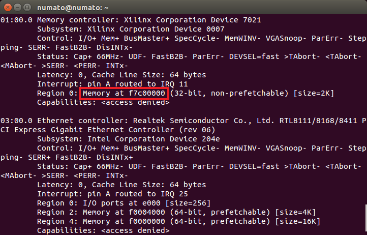
Download the complete pcimem application code zip file and unzip it in a specific location. Go to the command line terminal and check the PCIe base address by using the command
lspci -vv the output of the command is shown below. Make sure the HSFPX002 Board is inserted correctly into the PCIe Slot of the host system’s motherboard. If the host is unable to detect HSFPX002 (which should show up as “Memory controller: Xilinx Corporation Device 7021” as in the image below), make sure the board is inserted correctly into PCIe Slot and do a soft reset after the host is powered up. A soft-reset after the host is powered up helps the host detect FPGA-based PCIe devices.
Step 2:
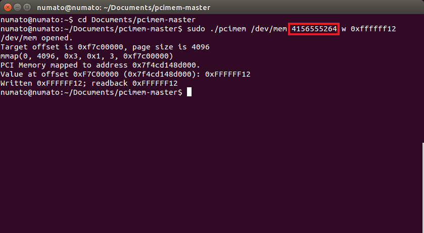
In the command line terminal, open the path where you saved the ‘pciemem’ code. First, compile the C program by using the command “make”. Once it is compiled successfully, use the following command:
sudo ./pcimem /dev/mem 4156555264 w 0xffffff12
Here,
4156555264: indicates the base address + offset, it is the address to which write is performed and it is the decimal value of hex: 0xf7c00000 (in the above image)
w: indicates whether it is a word, a byte, or a half word.
0xffffff12: 32-bit data value for write purpose.
You will observe the following output indicating that the 32-bit data has been written to the specified address and read back from it. If the written data matches the data read, it means data was successfully written to HSFPX002.
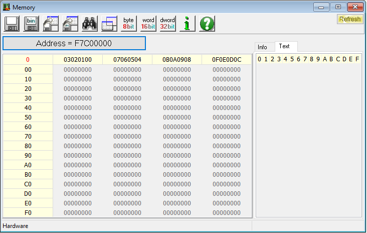
Communicating with the Tagus via PCI Express on Windows Machines:
Step 1:
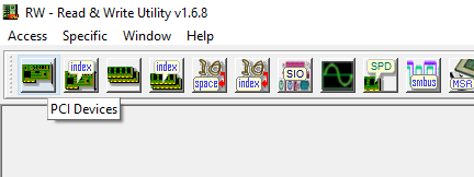
For Windows machines, use RW-Everything software to write data.
Step 2:
Insert HSFPX002 board in the PCIe slot of the host system’s motherboard. Open RW-Everything, Click PCI Devices. It will open PCI Devices.
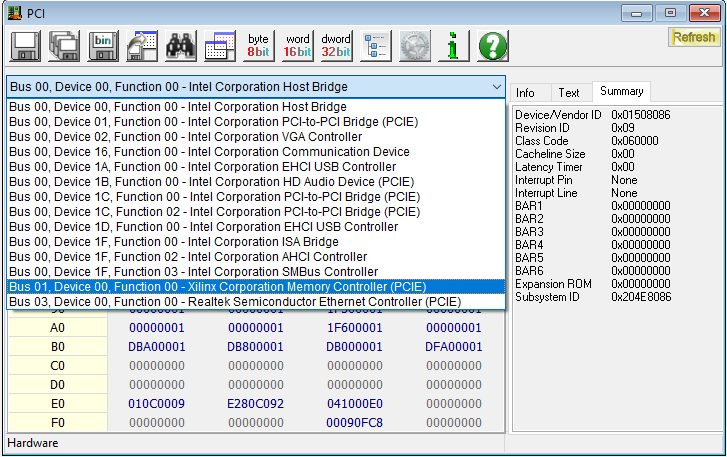
Step 3:
Select Xilinx PCIe Device from the drop-down list.
Step 4:
Locate the BAR Address from the addresses on the left side.
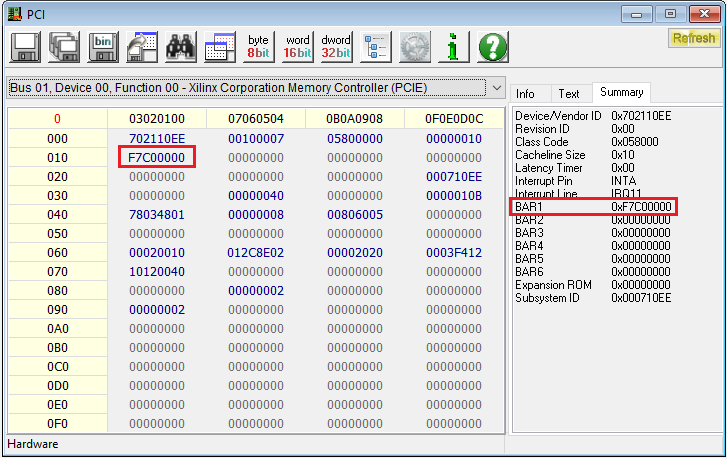
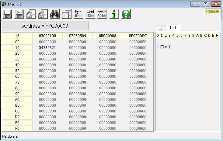
Step 5:
Double-click to open the BAR Address and select any one of the address bits and write some data to it. The data is retained even if you close and open the application indicating that the write operation is successful.