Introduction
In computer hardware, Direct Memory Access (or DMA) is a feature that allows peripheral devices to access main memory, without burdening the processor. PCIe stands for “Peripheral Component Interconnect Express”, and is a serial expansion bus standard for interconnecting peripheral devices, as the name suggests. In this article, we will see how to implement a simple design to read and write data to Aller Artix-7 FPGA Board which acts as a PCI Express endpoint device. Aller features an M.2 form factor M-key slot which is a computer storage interface based on the PCI Express standard. We will use Xilinx’s DMA for PCI Express (PCIe) Subsystem or XDMA IP core in this example design. We will also demonstrate the PCIe DMA functionality in this article.
Prerequisites:
Hardware:
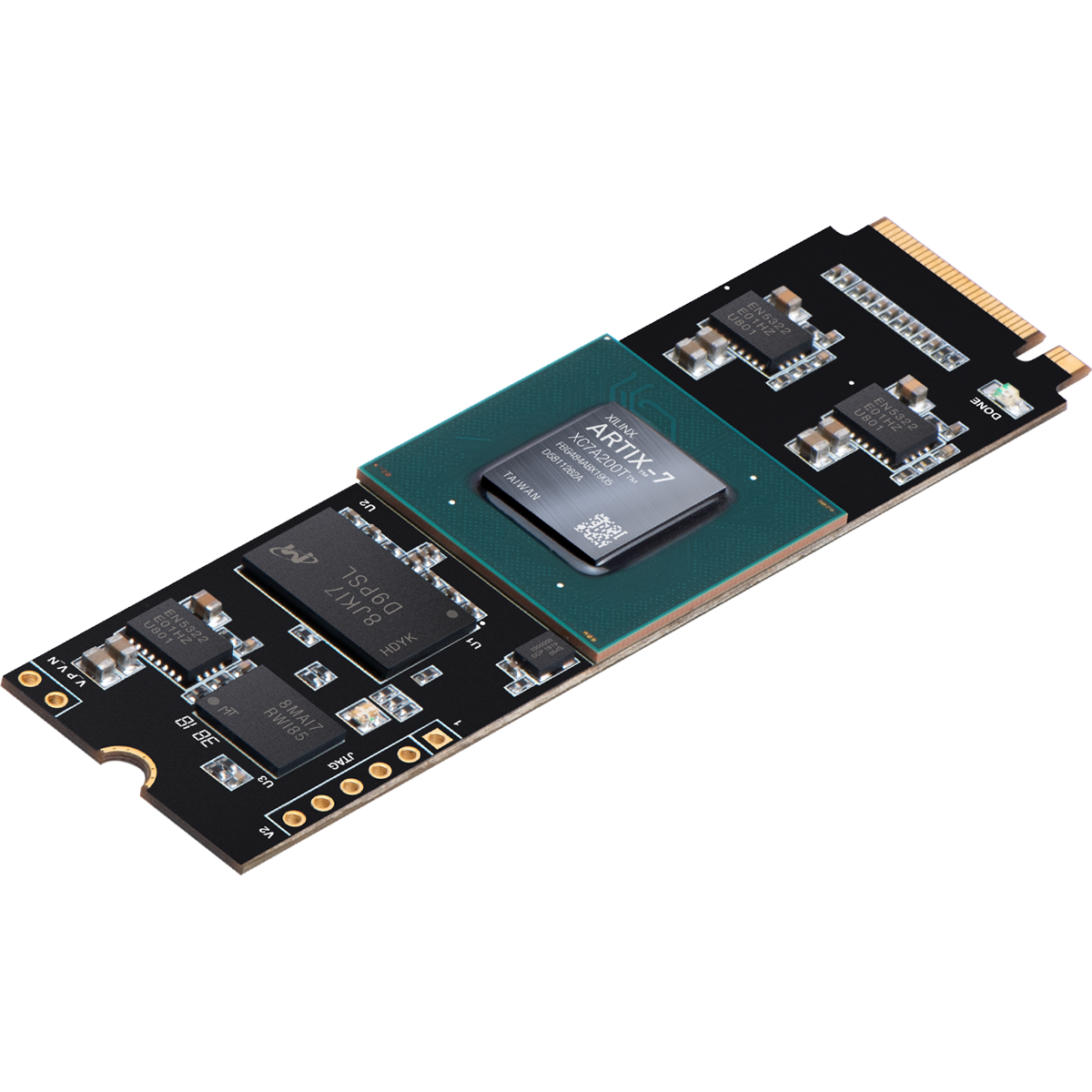
- Aller Artix-7 FPGA Board with M.2 Interface
- Xilinx Platform Cable USB
- Host PC with Linux or Windows (Linux preferred)
Software:
- Vivado Design Suite with SDK installed (2018.2 or higher)
Creating PCIe DMA Design in Vivado
The following steps will walk you through the process of creating a new project in Vivado and implementing a PCIe DMA example design for Aller using the XDMA IP core. Screenshots are added wherever possible to make the process easier for the reader.
Step 1:
Download and install the Vivado Board Support Package files for Aller from here. Follow the README.md file on how to install Vivado board support files for Numato Lab boards.
Step 2:
Open the Vivado Design suite, go to “File->Project ->New” to create a new project. The “New project” window will pop up. Click “Next”.
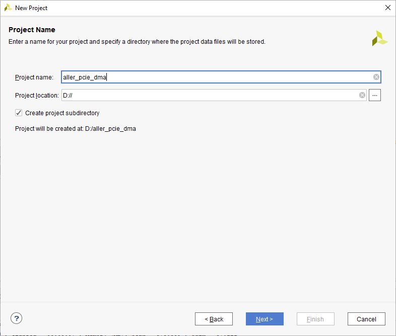
Enter an appropriate name for the project and choose a suitable location. Select the “Create project subdirectory” checkbox and click “Next” without making any changes until you see the “Default Part” page.
Step 3:
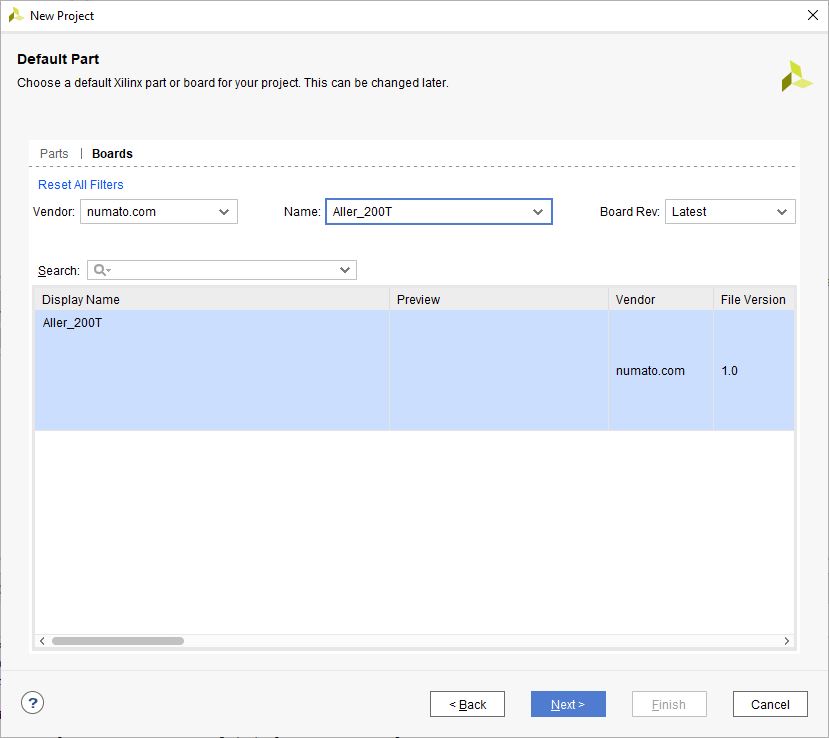
On the “Default Part” page, select the “Boards” tab. Choose the Vendor as “numato.com” and select “Aller_200T” from the list of boards as shown below. If “Aller_200T” is not listed, make sure that the board support files are installed correctly. Click “Next” to continue.
Click “Finish” to complete creating a new project. A new project will be created by Vivado with the selected settings.
Step 4:
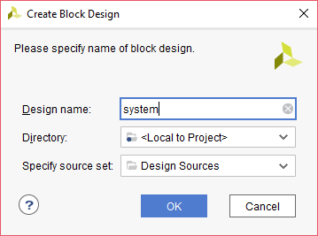
Under the “Flow Navigator” panel, select “Create Block Design” under the IP Integrator section. Enter a name for the block design and click “OK”. An empty block design will be created.
Step 5:
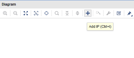
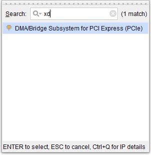
In the “Diagram” window, click “Add IP” (refer to the image below) and search for “XDMA”. You will find “DMA/Bridge Subsystem for PCI Express (PCIe)“, click “Enter” to add the IP to the block design.
Step 6:
We have to configure the XDMA IP for our example design for Aller. Double-click on the IP to customize it as follows.
- In the Basic tab, under the PCIe Interface, change
Lane WidthtoX4andMaximum Link Speedto5.0GT/s.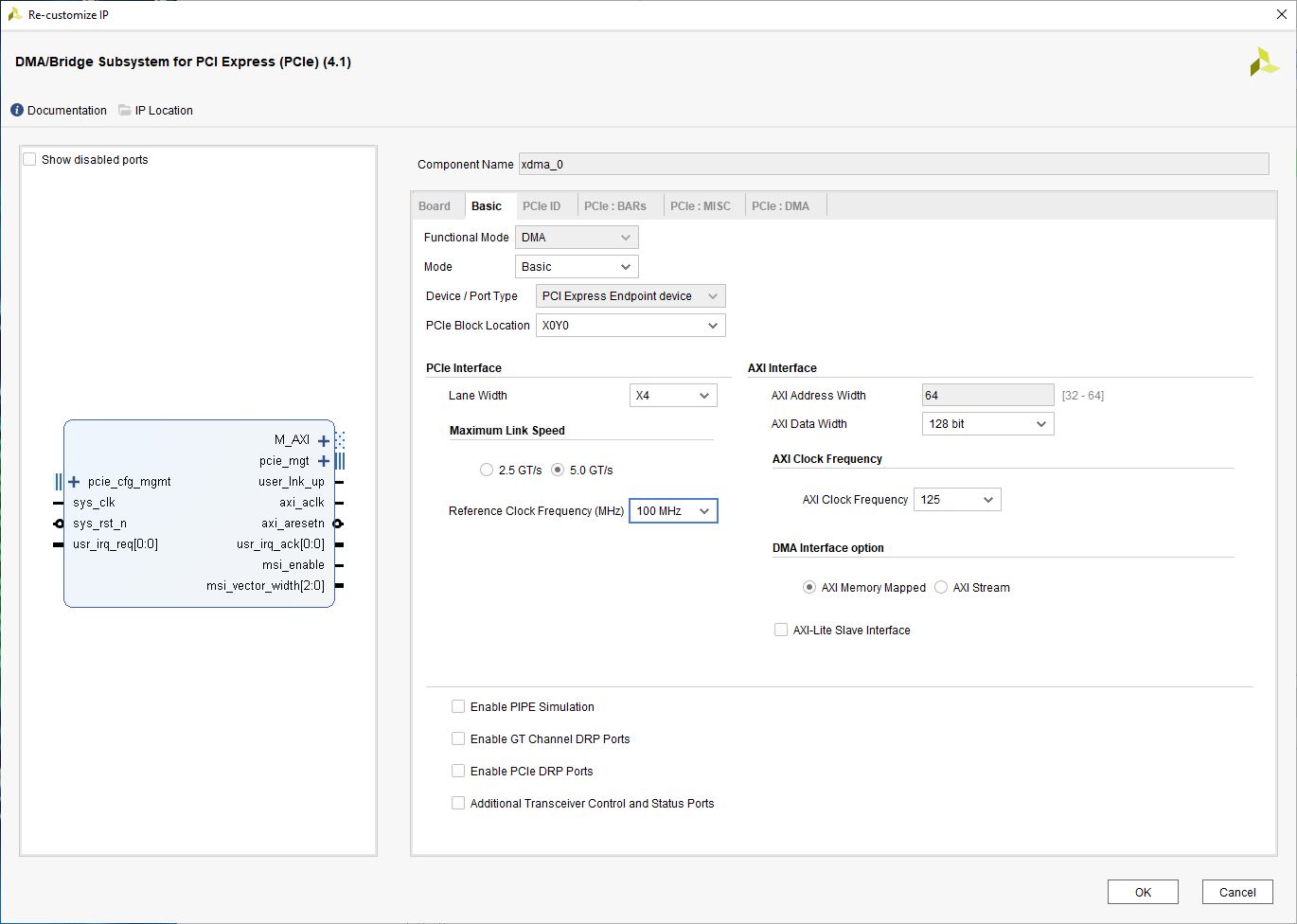
- In the PCIe:BARs tab, enable the
PCIe to AXI Lite Master Interface.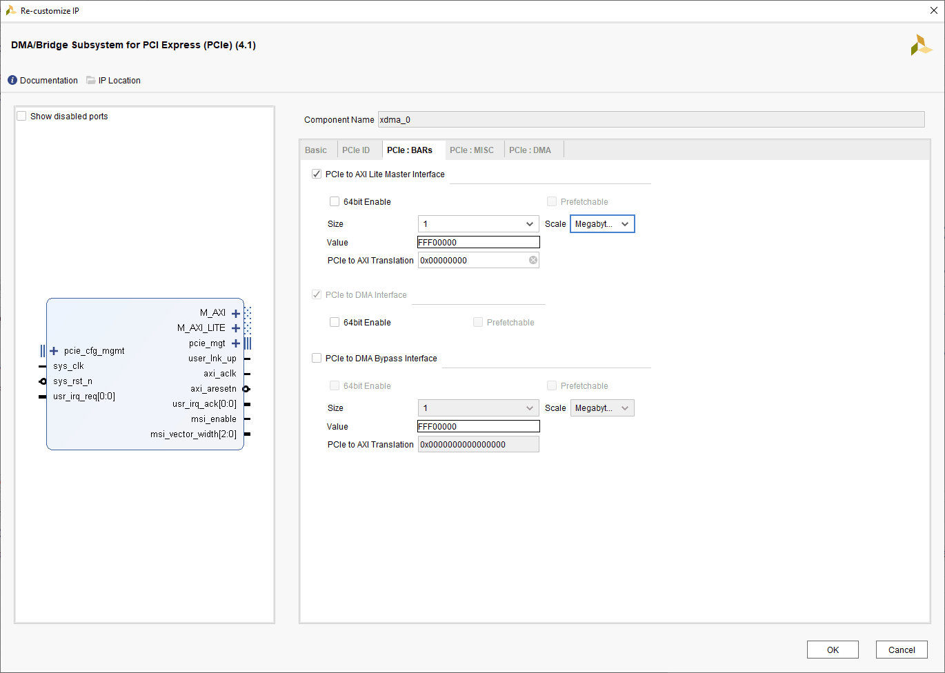
- In the PCIe: MISC tab, disable the
Configuration Management Interface.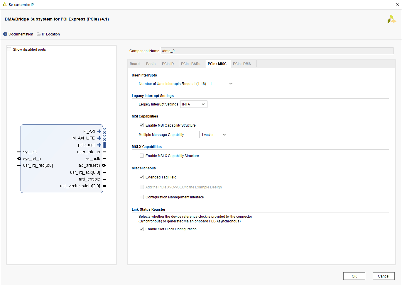
- In the PCIe:DMA tab, change the
Number of DMA Read Channel (H2C)andNumber of DMA Write Channel(C2H)to2.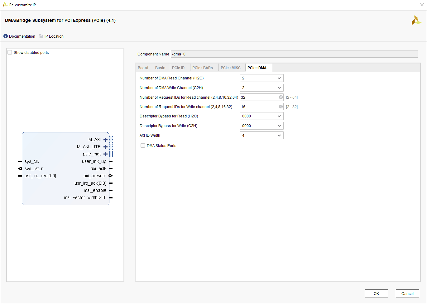
Click “OK” to customize the IP.
Step 7:
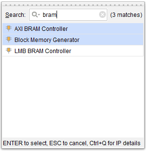
Again, click “Add IP” in the “Diagram” window and search for “AXI BRAM Controller” and “Block Memory Generator” as shown below. Drag and drop the IPs to the design.
Step 8:
Double-click on “Block Memory Generator” to customize it. In the Basic tab, select the Memory Type as True Dual Port RAM.
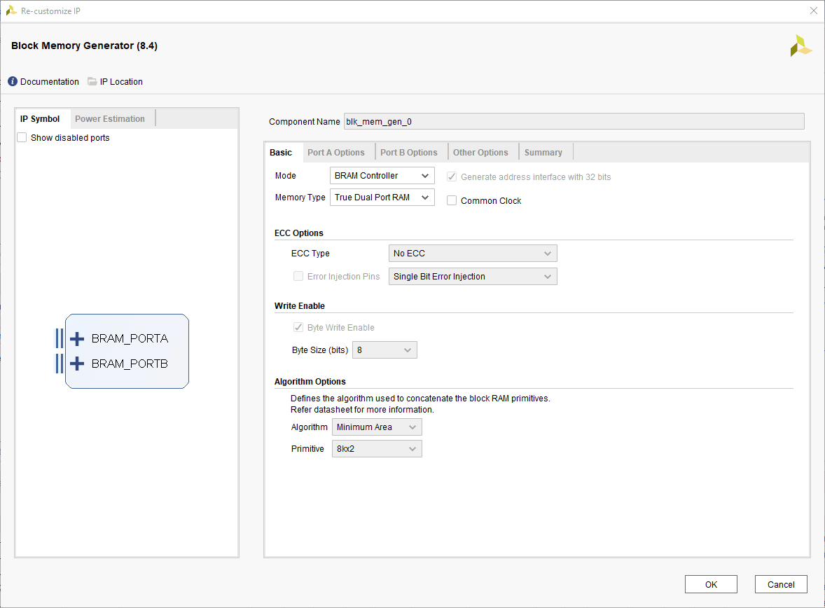
Under the Other Options tab, uncheck the “Enable Safety Circuit” checkbox.
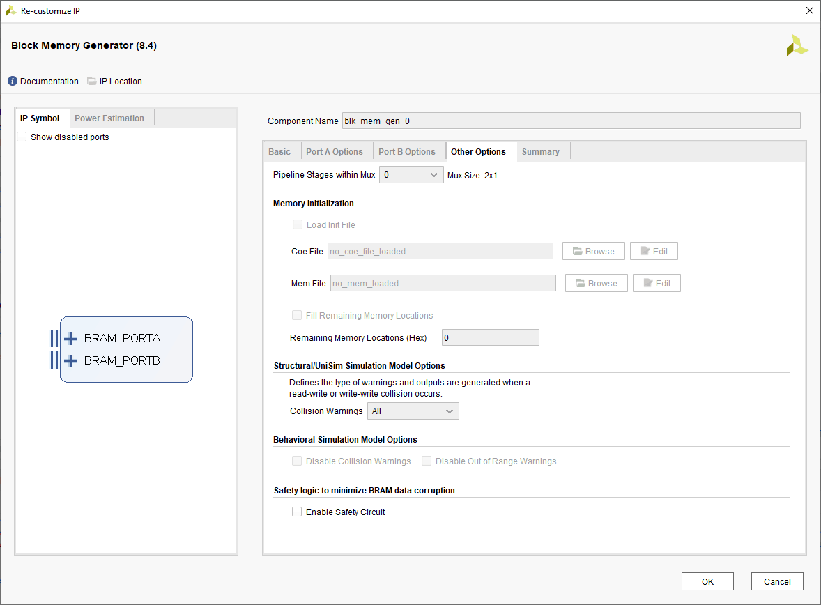
Click “OK” to customize the IP.
Step 9:
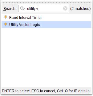
We will now add “Utility Vector Logic” to the design. Click “Add IP” and search for Utility Vector Logic as shown below. Drag and drop the IP to the design.
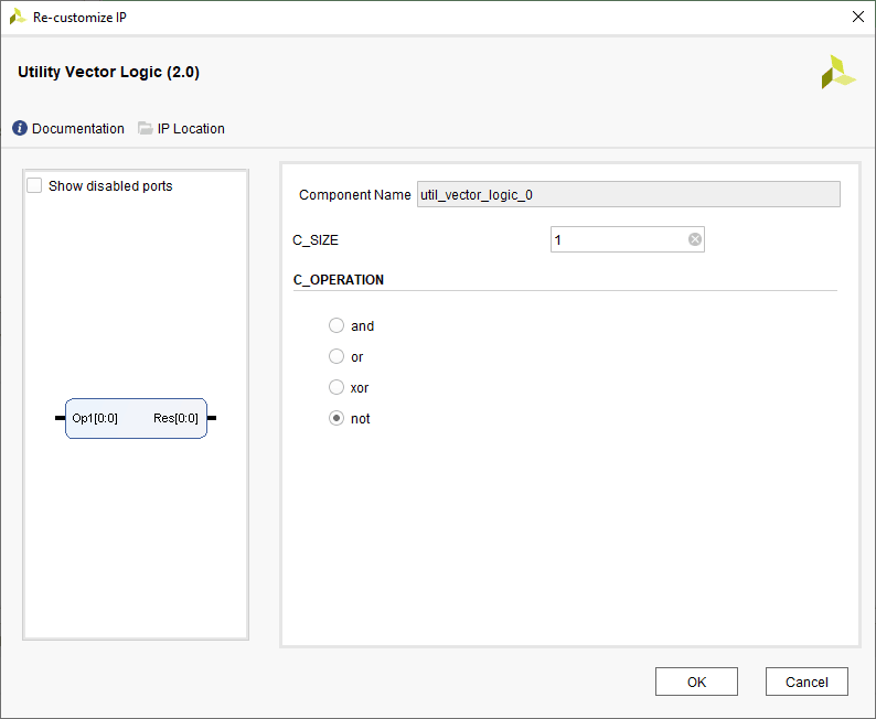
Double-click on the IP to customize it as shown in the image below. Change C_SIZE to 1 and C_OPERATION to “not”. Click “OK” to customize the IP.
Step 10:
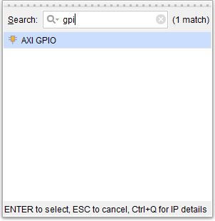
Finally, we will add “AXI GPIO” to the design. Click “Add IP”, type GPIO in the search box and add “AXI GPIO” to the design window.
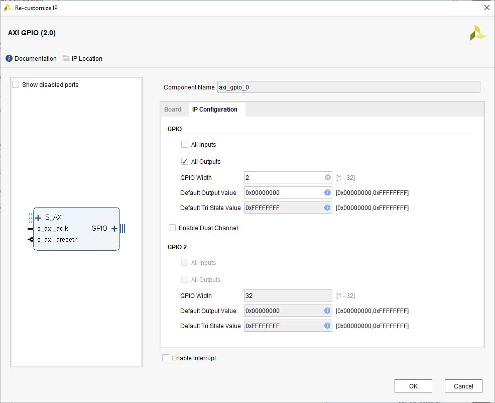
Double-click on the IP and customize it to give a 2-bit output as shown below. In the IP Configuration tab, enable “All Outputs” and change the GPIO Width to 2. We will connect this GPIO port to the red and blue LEDs in Aller.
Step 11:
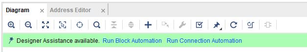
Having added all the required blocks, let’s make use of “Designer Assistance” from Vivado.
Click “Run Block Automation” and select the “All Automation” checkbox in the window that follows. Under the “Options” tab, select 1 Megabytes for the “PCIe to AXI Lite Master Interface” option. Make sure that the settings are as shown below.
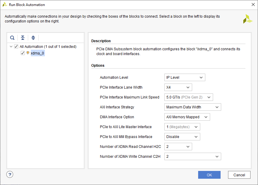
Click “OK” for Vivado to automatically configure the blocks for you.
Step 12:
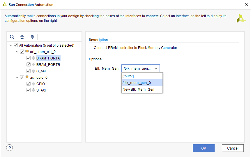
Click “Run Connection Automation”. In the Run Connection Automation window, select the “BRAM_PORTA” interface and change Blk_Mem_Gen under “Options” to /blk_mem_gen_0 as shown in the image below. Repeat the same for “BRAM_PORTB” and click “OK”.
Step 13:
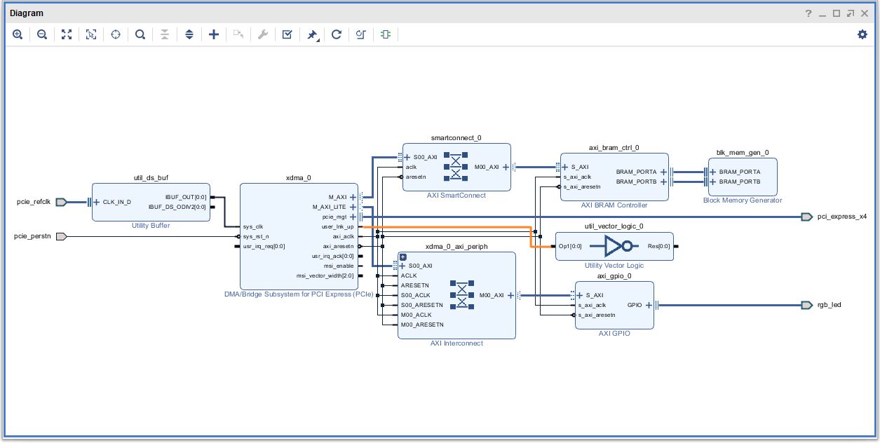
The XDMA IP core has a user_lnk_up output port which indicates that the PCIe core is linked up with a host device. Connect this pin to the input of “Utility Vector Logic” as shown below.
Step 14:
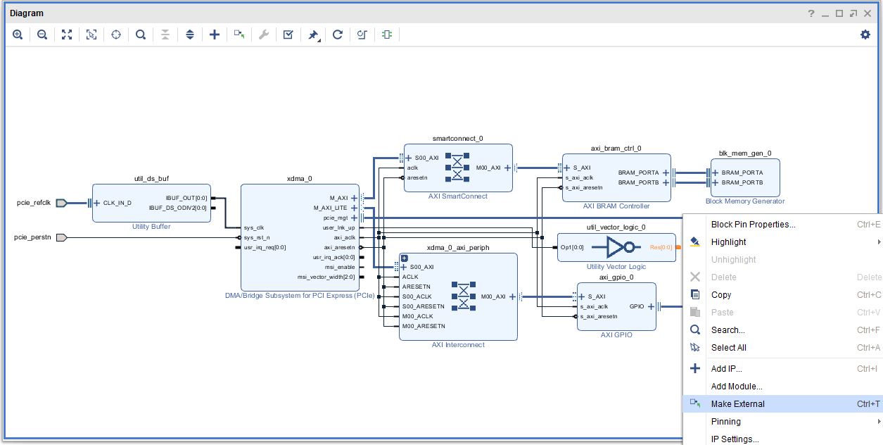
We will connect the output of “Utility Vector Logic” to the green LED in Aller. Right-click on the output pin and select “Make External” as shown below.
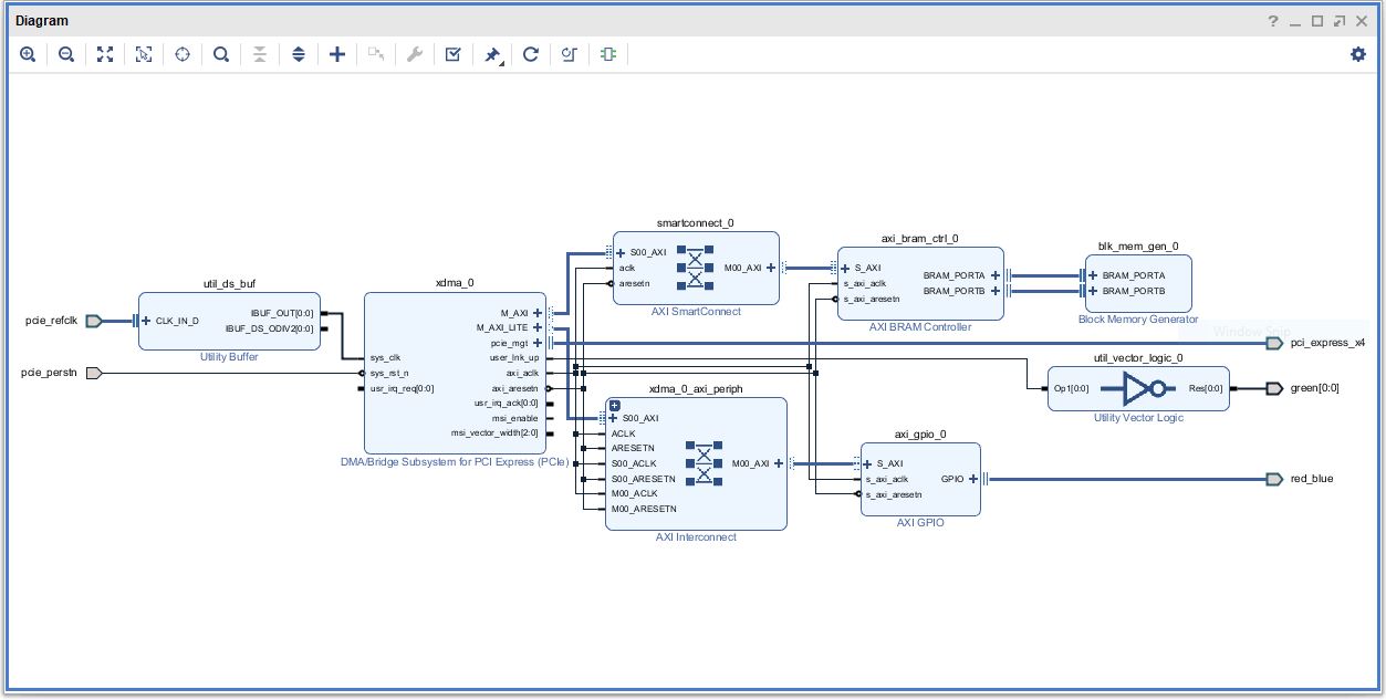
The final design should look similar to the image below (rename the ports appropriately).
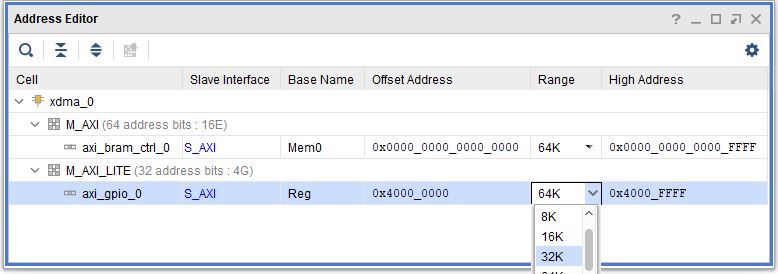
Step 15:
In the “Address Editor” tab, change the Offset Address and Range of axi_bram_ctrl_0 to 0x0000_0000_0000_0000 and 64K respectively. Also, change the Range of axi_gpio_0 to 32K as shown in the following image.
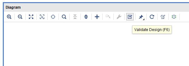
Step 16:
Now that the design is complete, validate the design to ensure that the connections are correct.
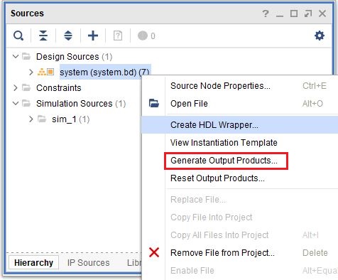
Step 17:
Right-click on the block design file in the “Sources” window, select “Create HDL Wrapper” and click “OK” in the dialog box that follows, to let Vivado generate a wrapper for you. Then select “Generate Output Products”.
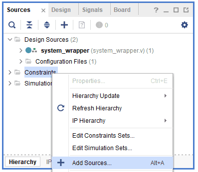
Step 18:
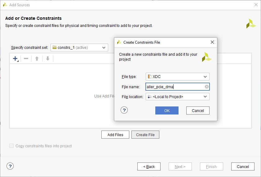
We have to add constraints for some ports in the design. Since we have BSP, most of the ports would be assigned from the BSP. We will have to manually assign for the rest of the ports. Right-click on “Constraints” in the Sources window, and select “Add Sources” as shown below.
In the window that follows, select “Add or create constraints” and click “Next”. On the following page, select “Create File” and give an appropriate name to the constraints file, as shown below. Click “Finish”.
Step 19:
Copy the following constraints to the newly created constraints file.
set_property -dict {PACKAGE_PIN AB22 IOSTANDARD LVCMOS33 SLEW FAST} [get_ports green]
set_property -dict {PACKAGE_PIN AB21 IOSTANDARD LVCMOS33 SLEW FAST} [get_ports {red_blue_tri_o[0]}]
set_property -dict {PACKAGE_PIN U20 IOSTANDARD LVCMOS33 SLEW FAST} [get_ports {red_blue_tri_o[1]}]

set_property BITSTREAM.CONFIG.CONFIGRATE 16 [current_design]
set_property BITSTREAM.GENERAL.COMPRESS TRUE [current_design]
set_property BITSTREAM.CONFIG.SPI_BUSWIDTH 4 [current_design]
Important:
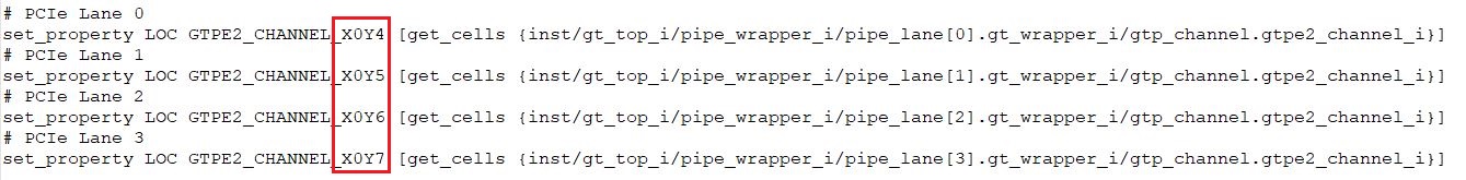
Go to the project folder, and browse to the file system_xdma_0_0_pcie2_ip-PCIE_X0Y0.xdc located at the aller_pcie_dma.srcs\sources_1\bd\system\ip\system_xdma_0_0\ip_0\source folder (the folder names may vary depending on your project and design names). Open it in your favorite text editor and change the following site locations as shown in the image below.
Step 20:
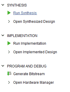
Select “Run Synthesis” under the “Flow Navigator” panel. If the synthesis is complete, proceed to select “Run Implementation”.
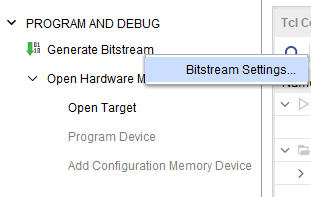
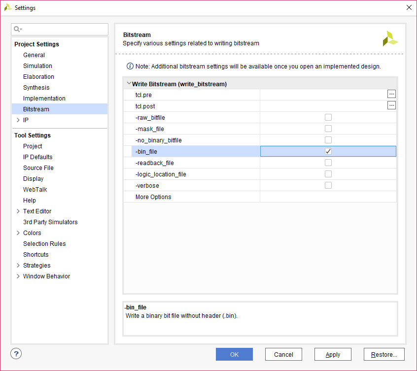
Before proceeding to generate the bitstream, right-click on “Generate Bitstream” under “PROGRAM AND DEBUG” in the “Flow Navigator” panel and select “Bitstream Settings”. Enable the -bin_file checkbox and click “OK”.
Step 21:
Once the bitstream is generated successfully, program Aller by following the steps mentioned under Programming QSPI Flash using Vivado in the product user manual.
Communicating with Aller via PCI Express on Linux Machine
In this section, we will discuss the steps involved in checking the DMA functionality and controlling the GPIOs (RGB LEDs) in the design using a Linux host.
Connect the Aller board into the PCIe slot and boot the Linux system. Before testing anything, let’s confirm that the board is detected over PCIe.
Open the Terminal and execute the following command:
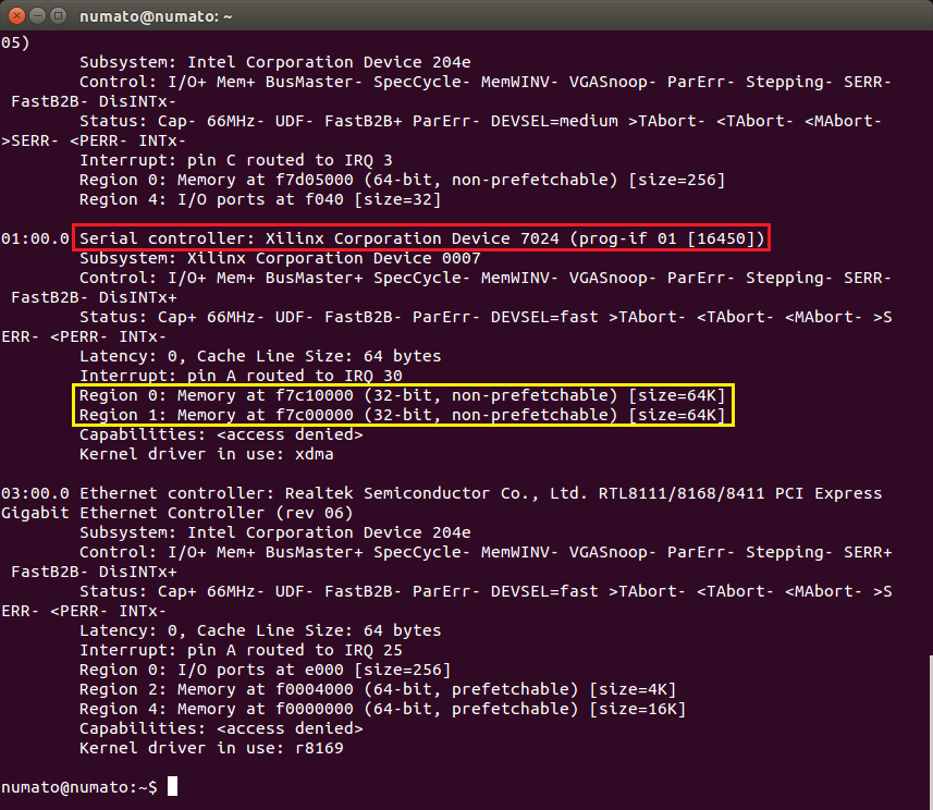
lspci -vv
If the Aller board is detected, it will show up as “Serial controller: Xilinx Corporation Device 7024” as shown in the image below.
If the host is unable to detect the board, make sure that it is inserted correctly into the PCIe slot and do a soft reset. A soft reset after the host is powered up, helps the host to detect FPGA-based PCIe devices.
You can take note of the PCIe base addresses which can be seen as in the image above. We will use this address to write data to Aller over PCIe.
Controlling the GPIOs:
Step 1:
Download the complete pcimem application code zip file and unzip it in a specific location. In the Terminal, change the directory to that location. The following is the command used in the author’s case:
cd Desktop/pcimem-master
Compile the C program by executing the command:
make
Step 2:
Once it is compiled successfully, run the following command:
sudo ./pcimem /dev/mem 4156620800 b 0x01
Here,
4156620800: is the base address + offset. It is the address to which the write is performed and is the decimal value of hex: 0xf7c10000.
b: indicates whether the data to be written is a word [w], a byte [b], or a half-word [h].
0x01: 8-bit data value to be written to the device.
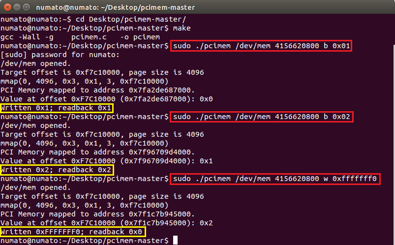
The image above shows the output corresponding to different values written to the device. It indicates that the last 2 bits of data have been written to the specified address and read back from it. If the written data matches the data read, it implies that the data was successfully written to the Aller and we can also observe the corresponding output on the LEDs. Here, the last 2 bits are taken for the output on red & blue LEDs.
Checking the DMA functionality:
Step 1:
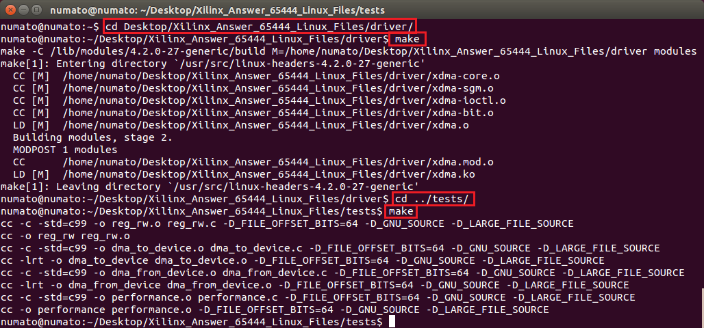
Download the Xilinx Answer 65444 files for Linux from here and save them in a convenient location. In the Terminal, change the directory to /Xilinx_Answer_65444_Linux_Files/driver/ folder and compile the C program by executing the command make.
Once the compilation is completed, change the directory to /Xilinx_Answer_65444_Linux_Files/tests/ folder and execute the “make" command to compile the C program in that folder.
Step 2:
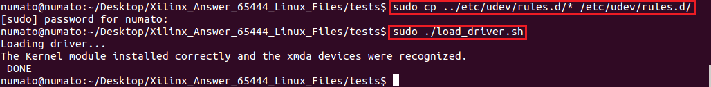
We have to copy the driver rules to the /etc/ directory of the system. So, run the following command:
sudo cp ../etc/udev/rules.d/* /etc/udev/rules.d/
You might be required to enter the password of the Linux User to execute this command.
After the files are copied, let’s load the driver using the following command:
sudo ./load_driver.sh
Step 3:
We can now test the DMA. This can be done by running the script “run_test.sh” using the following command:
sudo ./run_test.sh
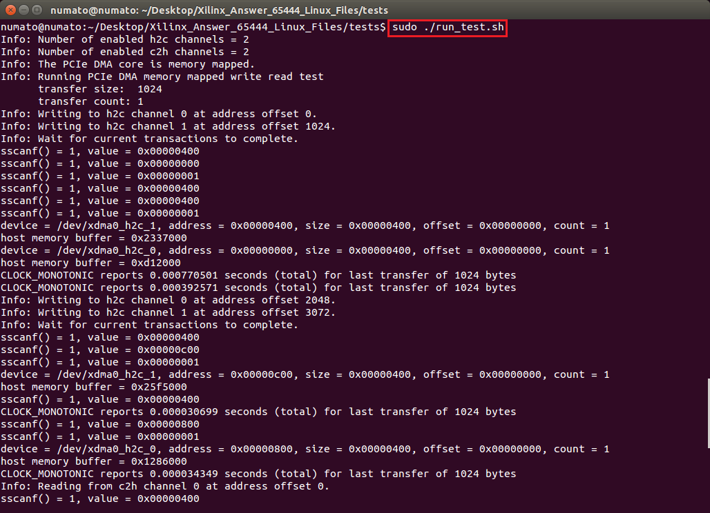
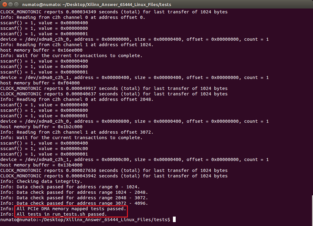
If the tests in “run_test.sh” pass without any errors, you will see a message that says “All tests in run_tests.sh passed.”, as shown in the image above.