Introduction
Aller is specifically designed for the development and integration of FPGA-based accelerated features into other larger designs, it can be used with laptops, desktops, and servers featuring standard 2280 M.2 form factor M-key slot.
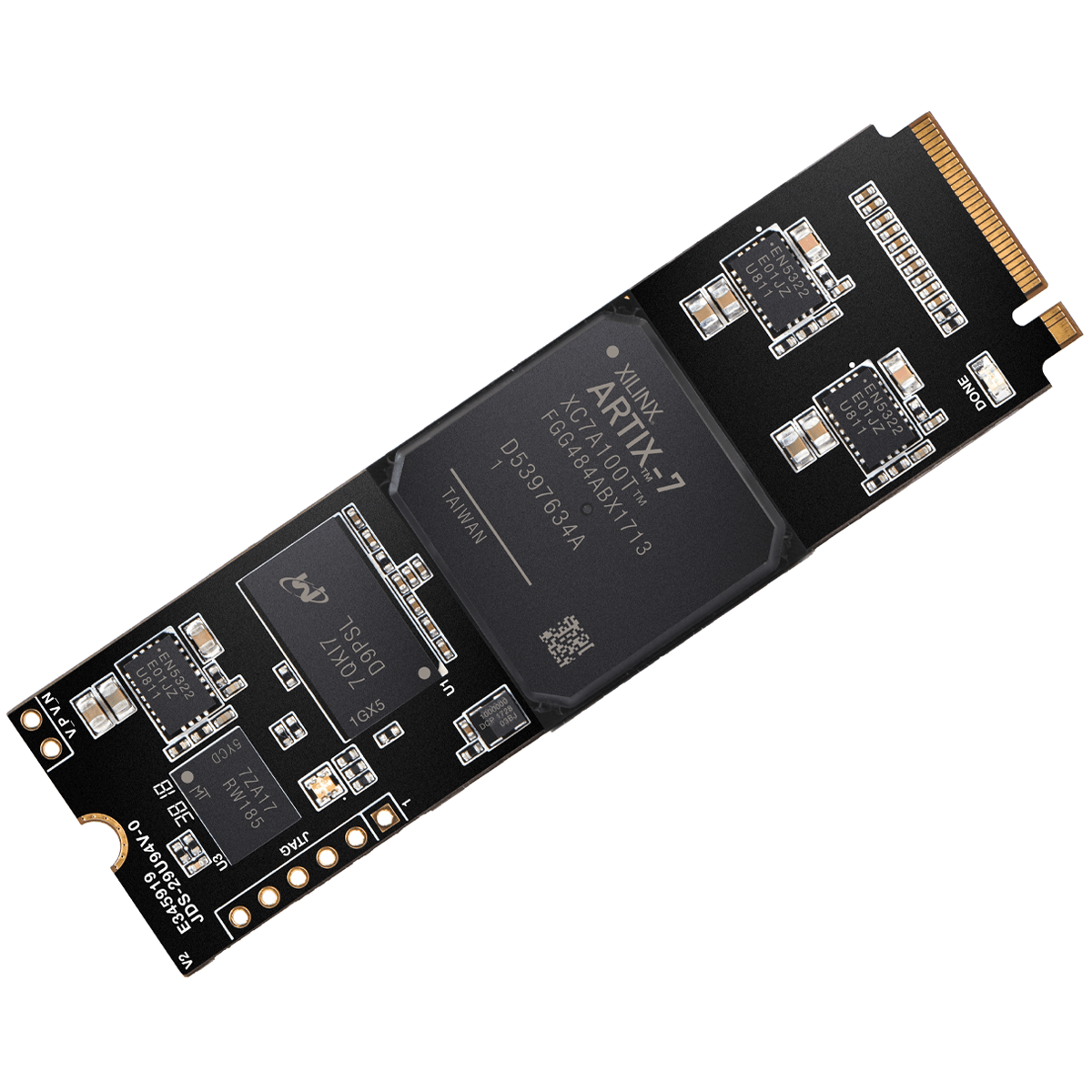
Aller is an easy-to-use M.2 form-factor FPGA Development Board featuring Xilinx Artix-7 FPGA with x4 PCIe Gen2 lanes on M.2 M-Key interface, Trusted Platform Module (TPM AT97SC3205), 2Gb DDR3 SDRAM and 512Mb QSPI Flash Memory.
Nowadays, most new laptops come with M.2 M-key slots for NVMe storage modules and Aller can be seamlessly used with those slots. Open source PCI Express IP cores such as litepcie make the development of PCIe designs very cost-effective. The M.2 M-Key provides up to 4x PCIe lanes, each running at 5 GT/s (PCIe Gen 2) on Aller.
Board Features
- Device: Xilinx Artix 7 FPGA (XC7A200T-2FBG484I)
- DDR3: 2Gb DDR3 ( MT41J128M16JT-125:K TR )
- 4 lane PCIe Gen2 (5 GT/s)
- Onboard 512Mb QSPI flash memory for FPGA configuration (S25FL512SDSBHV210/IS25LP512M-RHLE)
- JTAG header for programming and debugging
- 100 MHZ CMOS oscillator
- 1 x Trusted Platform Module (AT97SC3205)
- M.2 Connector Interface, M-Key
- Powered from M.2 connector
- 1 RGB LED for custom use
Applications
- Product Prototype Development
- Accelerated computing integration
- Development and testing of custom embedded processors
- Signal Processing
- Memory Intensive FPGA development
- Educational tool for Schools and Universities
- High Hash Rate calculations for Blockchain technologies such as Bitcoin and Ethereum
- Offloading computationally intensive algorithms to FPGA
- Machine Learning and Artificial Intelligence
How to use Aller Artix 7 FPGA Module
The following sections describe in detail how to use this module.
Hardware Accessories Required
Along with the Aller module, you may need the items in the list below for easy and fast installation.
- A Xilinx Platform Cable USB II compatible JTAG programmer.
Connection Diagram
This diagram should be used as a reference only. The schematics are available at the end of this document for detailed information.
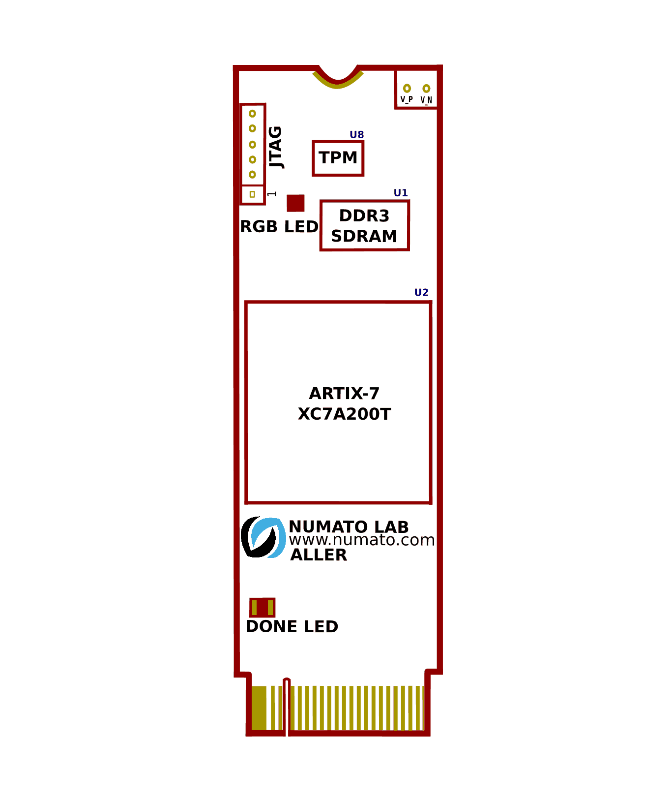
Note: TPM is at the bottom side of the board.
Power
Aller requires +3.3V power supply to function properly. Aller takes power from M.2 connector. Current requirement for this board largely depends on your application.
Temperature and Heat Dissipation
M.2 form-factor doesn’t permit thick and large surface-area PCBs, so heat dissipation in M.2 profile modules is always a challenge. M.2 modules are traditionally used with application specific ICs for WiFi, USB etc, and the heat dissipation in those are comparatively lesser whereas in case of FPGAs, heat dissipation and power requirements are higher.
Aller features an Artix-7 200T FPGA with -2I speed grade (-40°C~100°C range) and 800Mbps DDR3 RAM. When running at maximum FPGA resource utilization and DDR3 running at max 800 Mbps, huge amount of heat is dissipated. PCB thickness and surface area being low, the junction temperature of FPGA can rise to a high value. FPGA would get damaged if junction temperature rises above 100 °Celsius.
Therefore, heat sink is mandatory when using Aller with heavy designs. Else, the FPGA and the board may get damaged. Heat sinks with good thermal coupling have been tested to decrease the temperatures by 15-20°C. If the temperature still approaches dangerous zone, then forced air cooling using fans might be required.
Aller ships with a standard heat sink which should be sufficient for most use cases. It should be noted that with the addition of heat sink, the module may not fit inside some space constrained cases such as thin laptops. For simpler designs running at lower frequency and not using DDR3, the heat dissipation is less, and heat sink is not compulsorily required. It is expected that users do their own independent power analysis using Xilinx Power Estimator to find out the optimal cooling requirements for Aller.
We recommend maintaining the junction temperature of FPGA below 90°C range. Users can use XADC block inside Artix-7 FPGAs to measure temperature.
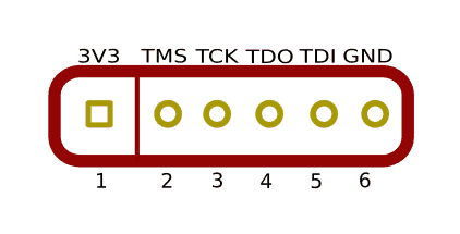
JTAG Connector
JTAG connector allows the FPGA’s JTAG registers to be accessed using a JTAG cable, compatible with Xilinx Platform Cable USB. Use this header, to attach JTAG cable for programming and debugging.
RGB LED
Aller features one RGB LED which can be used for custom or debug purposes.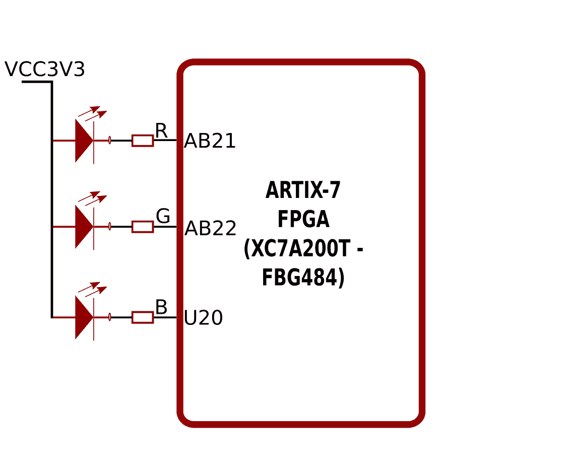
Trusted Platform Module(TPM)
The Trusted Platform Module(TPM) is an integrated security module for hardware authentication. The security module is used primarily for cryptographic key generation, key storage and key management as well as generation and secure storage for digital certificates.
Trusted Platform Module(TPM)
| Signal Name | Artix-7 (FBG484) Pin |
|---|---|
| TPM_MOSI | Y19 |
| TPM_MISO | V18 |
| TPM_CS# | Y18 |
| TPM_CLK | W20 |
| TPM_RST# | V19 |
M.2 Edge Connector
M.2 edge-connector on Aller provides the power to the board. Each lane is capable of 5GT/s resulting in maximum theoretical data transfer rate of 2 GB/s for all 4 lanes combined.
M.2 Edge Connector
| Signal Name | Artix-7 (FBG484) Pin |
|---|---|
| REFCLK_P | F6 |
| REFCLK_N | E6 |
| M2_TX0_P | B4 |
| M2_TX0_N | A4 |
| M2_TX1_P | D5 |
| M2_TX1_N | C5 |
| M2_TX2_P | B6 |
| M2_TX2_N | A6 |
| M2_TX3_P | D7 |
| M2_TX3_N | C7 |
| M2_RX0_P | B8 |
| M2_RX0_N | A8 |
| M2_RX1_P | D11 |
| M2_RX1_N | C11 |
| M2_RX2_P | B10 |
| M2_RX2_N | A10 |
| M2_RX3_P | D9 |
| M2_RX3_N | C9 |
| M2_PERST# | AB20 |
| M2_CLKREQ# | AA19 |
| M2_WAKE# | V17 |
Generating Bitstream for Aller
HDL design needs to be converted to bitstream before it can be programmed to FPGA. Once the HDL is synthesized, it is easy to create a binary bitstream out of it. The bitstream can be generated for Aller in Vivado by following the steps below:
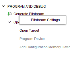
Step 1: It is recommended to generate .bin bitstream file along with .bit bitstream file. Right Click on “Bitstream Settings”.
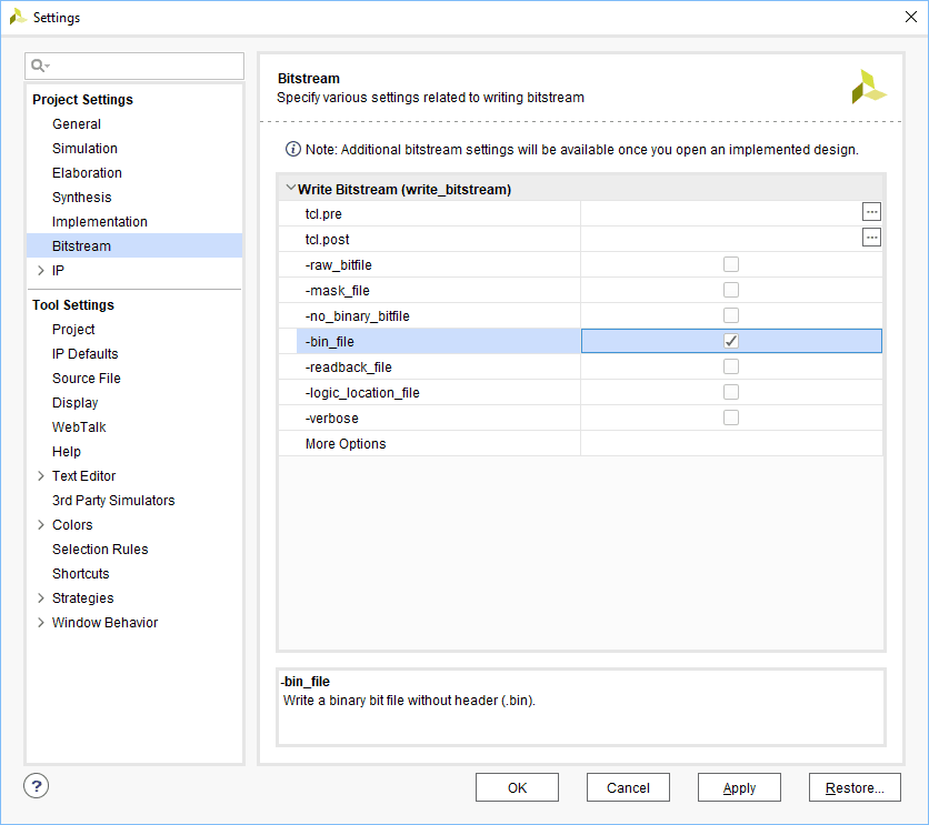
Step 2: Select “-bin_file*” option in the dialog window and Click “OK”.
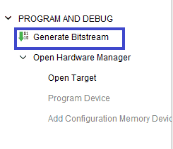
Step 3: Finally click “Generate Bitstream”.
Programming Aller Using JTAG
The onboard JTAG connector in the Aller Artix 7 FPGA Development Board facilitates easy reprogramming of SRAM and onboard SPI flash through JTAG programmer like “Xilinx Platform cable USB”. Following steps illustrate how to program FPGA on Aller using JTAG.
Step 1: Connect Xilinx Platform cable USB to Aller using JTAG cable. Power up Aller.
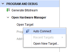
Step 2: Open Vivado project and open the target by clicking on the “Open Target” in “Open Hardware Manager” in the “Program and Debug” section of the Flow Navigator window. Select “Auto Connect”.
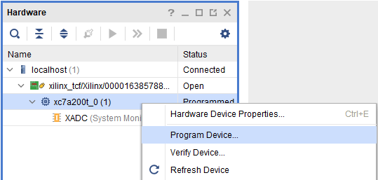
Step 3: If the device is detected successfully, then right click on the target device “xc7a200t_0” and select “Program Device” as shown below.
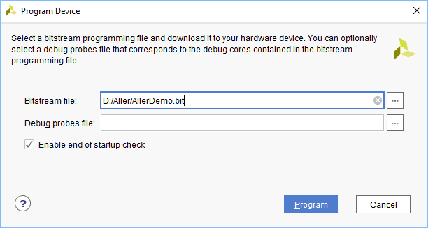
Step 4: In the dialog window which opens up, Vivado automatically chooses correct bitstream file if the design was synthesized, implemented and if bitstream was generated successfully. If needed, browse to the bitstream which needs to be programmed to FPGA. Finally click “Program”.
As soon as “Program” is clicked, a green colored LED (D1) on Aller should light up, indicating that programming process is going on. This LED will turn off when configuration is complete.
Programming QSPI Flash using Vivado
A ‘.bin’ or ‘.mcs’ file is required for programming Aller onboard QSPI flash.
Step 1: Open Vivado Project. Click on “Open Target” in “Open Hardware Manager” in the “Program and Debug’ section of the Flow Navigator window. Select “Auto Connect”.
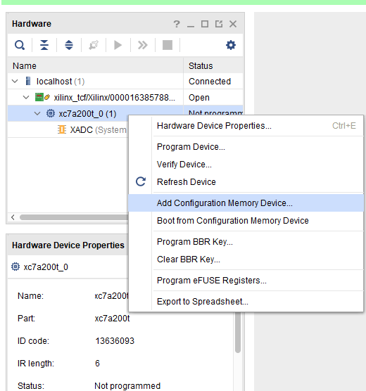
Step 2: If the device is detected successfully, then right-click on the target device “xc7a200t_0” and select “Add Configuration Memory Device” as shown below.
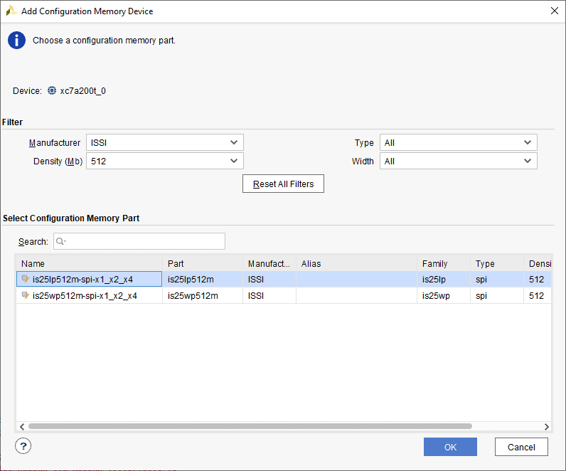
Step 3: Select the memory device “is25lp512m-spi-x1_x2_x4”, then click “OK”.
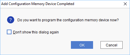
Step 4: After completion of Step 3 the following dialog box will open. Click “OK”.
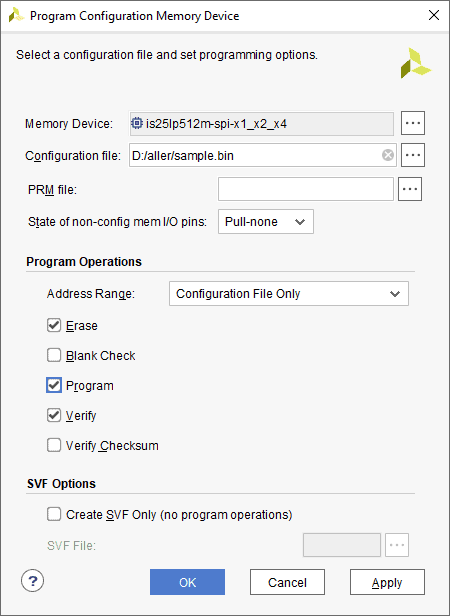
Step 5: Browse to the working ‘.bin’ file or the ‘.mcs’ file (whichever is applicable) and click “Apply” and then “OK” to program as shown below. If programming is successful, a confirmation message will be displayed.
Technical Specifications
| Parameter* | Value | Unit |
|---|---|---|
| Basic Specifications | ||
| DDR3 SDRAM (MT41J128M16JT-125) | 2 | Gb |
| On-board Oscillator Frequency (ASEM1-100.000Mhz-LC-T) | 100 | MHz |
| SPI Flash Memory (S25FL512SDSBHV210/IS25LP512M-RHLE) | 512 | Mb |
| Power Supply Voltage(External) | 3.3 | V |
| FPGA Specifications | ||
| Internal supply voltage relative to GND | -0.5 to 1.1 | V |
| Axuiliary supply voltage relative to GND | -0.5 to 2.0 | V |
| Output driver supply voltage relative to GND | -0.5 to 3.6 | V |
* All parameters considered nominal. Numato Systems Pvt Ltd reserves the right to modify products without notice.
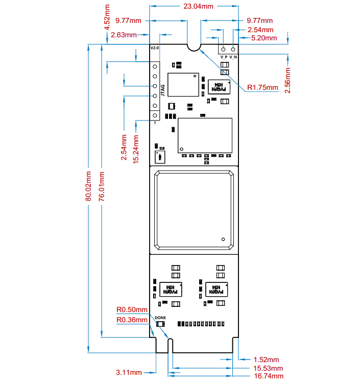
Mechanical Dimensions