Introduction:
Styx is an easy-to-use Zynq FPGA Module. Zynq SoC consists of Programmable Logic (PL) and Processing Subsystem (PS). SRAM programming of the PL part of Zynq is the same as other Xilinx 7 series FPGAs, but booting a bitstream from a flash is different in Zynq from other 7 series FPGAs. To boot a bitstream onto the PL part we need the help of Zynq Processing System IP and First Stage Bootloader Application. In this article, we will walk through all the steps from creating an RTL code for the PL part to programming a bitstream that will boot up from flash memory present on Styx FPGA Module.
SD Booting and QSPI Booting of Styx Zynq Module (PS design) from a non-volatile source are well explained in the article Styx: Boot from SD card and QSPI flash.
Prerequisites
- Hardware:
- Styx Zynq Module
- Micro USB cable
- Software:
- Xilinx Vivado Suite (version will change as per user)
- Tenagra FPGA System Management Software
Step 1:
Open Vivado Design Suite, go to File->Project->New. The New Project window will open. Click Next.
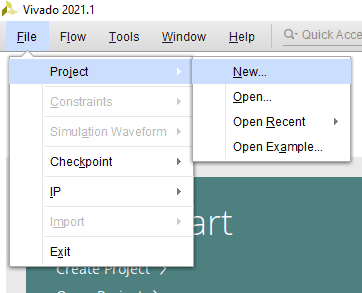
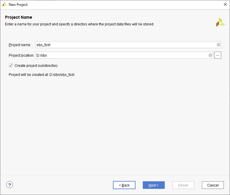
Enter a suitable name for the project and save it at a suitable location. Check the option “Create project subdirectory”. Click Next to continue.
Step 2:
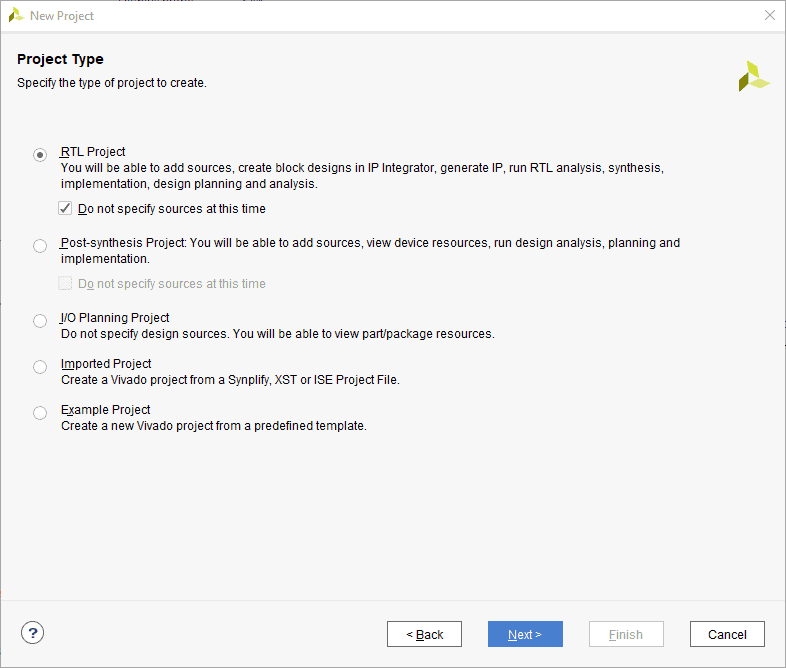
In the Project Type window, select RTL Project and check the “Do not specify sources at this time” option. Click Next.
Step 3:
In the Default Part window, select “Styx” from the Boards option. If Styx is not listed, make sure board support files are installed correctly. Click Next to continue.
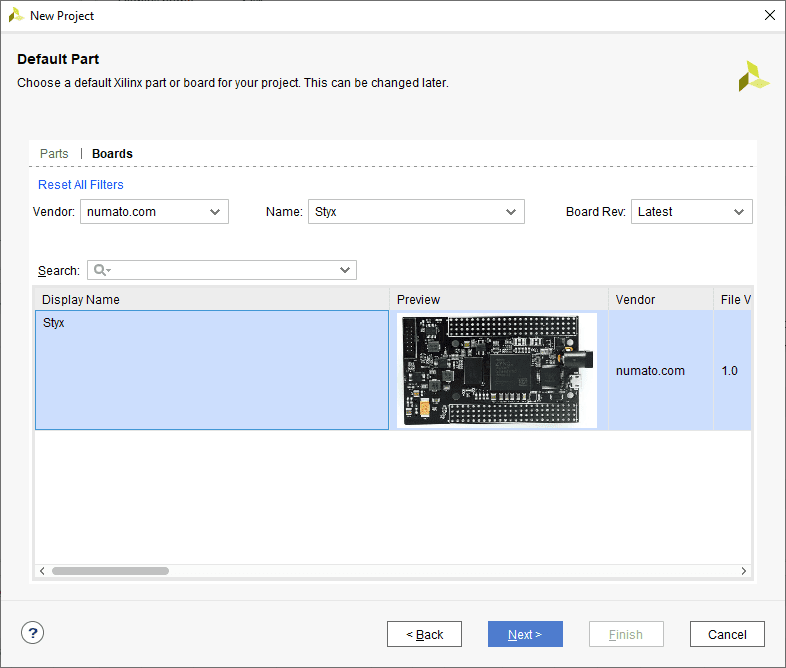
Click Finish to complete creating a new project. A new project will be created by Vivado with the selected settings.
Step 4:
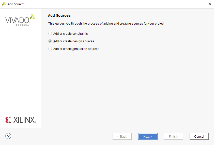
Select Add Sources under the Flow Navigator ->PROJECT MANAGER section. Now select “Add or create design sources” and click Next.
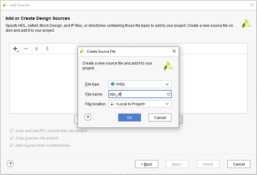
Now, select Create File. The Create Source File window will open, select the suitable File type and give the file name as in the image below. Click OK and then click Finish.
Step 5:
Provide the Verilog/VHDL module that wants to be implemented (here the author had given the VHDL program for GPIO all high)
Step 6:
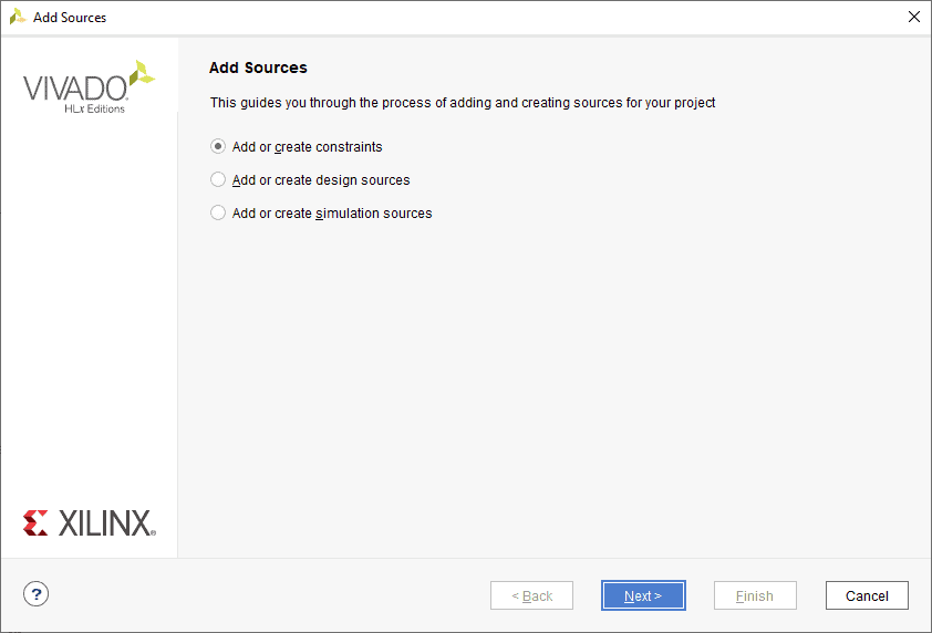
To create the constraints file, go to Add Sources under the Flow Navigator –> PROJECT MANAGER window, select the “Add or create constraints” and click Next.
Click on Create file and give a name for the XDC and select “File type” as XDC. Click OK and then Finish.
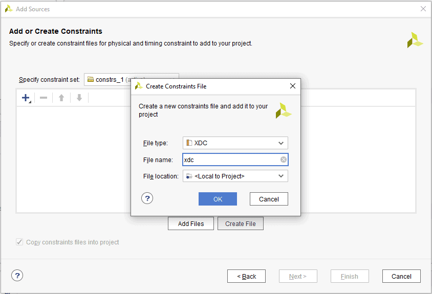
The XDC file is now created and is available in the Sources –> Constraints. Double click on it to open. Add the correct constraints for the design.
Step 7:
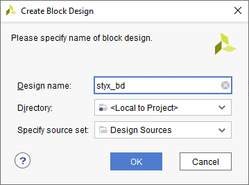
In the Flow Navigator panel, select Create Block Design under IP INTEGRATOR. Enter a name for the block design and click OK. An empty block design will be created.
Step 8:
Click Add IP,
![]()
Search for the ZYNQ7 Processing System and Add it.
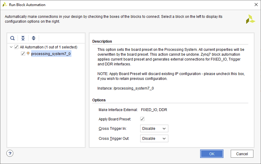
Step 9:
Click Run Block Automation, select All Automation and click OK.
Step 10:
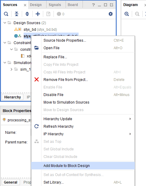
Go to Sources Tab, right-click on your Verilog or VHDL top module and select “Add Module to Block Design” which will add the RTL module to the block design.
Step 11:
Right-click the added module and select Make External.
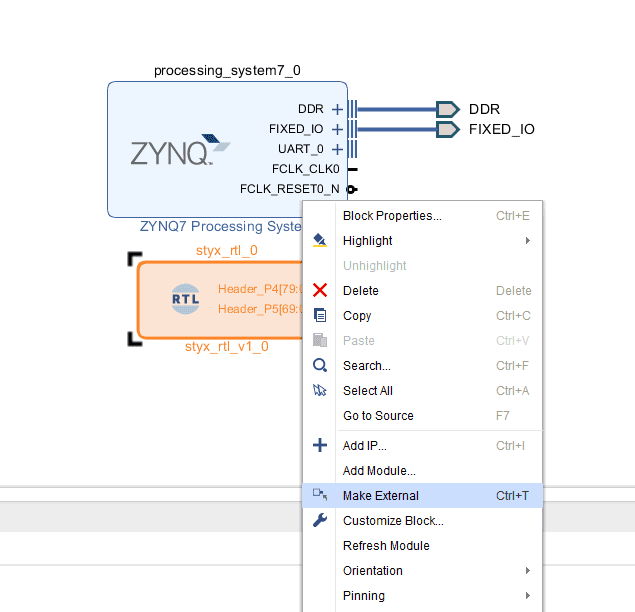
Make sure the external pins have the same naming as that of constraint pins.
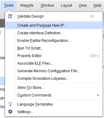
Step 12:
Select the Validate Design option from the Tools menu to ensure that connections are correct.
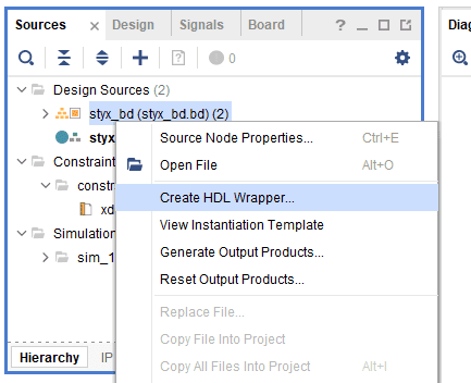
Step 13:
In the Sources window, right-click on the design and select Create HDL Wrapper. Click OK in the dialog box that appears.
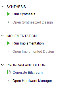
Step 14:
Click Generate Bitstream under the PROGRAM AND DEBUG section of Vivado to synthesize, implement and generate the bitstream.
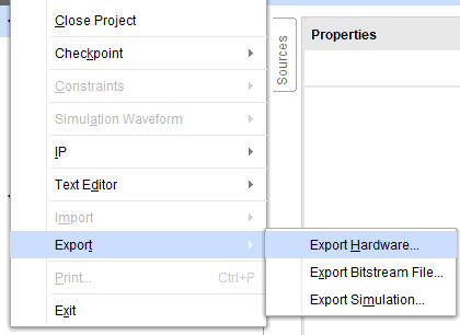
Step 15:
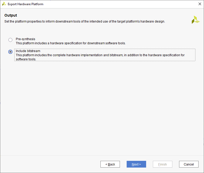
Once the bitstream is generated successfully, we need to export the hardware along with the bitstream. From the File menu, select Export -> Export Hardware.
Step 16:
Select “Launch Vitis IDE” from the “Tools“. Provide a “Workspace” directory and click “Launch”.
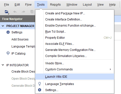
Note: In Vivado 2023.2, accessing Vitis via the tools menu inadvertently launches Vitis Unified instead of Vitis Classic, which is our preferred tool for project creation. To utilize Vitis Classic, it is necessary to launch it separately. This differentiation is applicable exclusively to versions released from 2023.2 onwards.
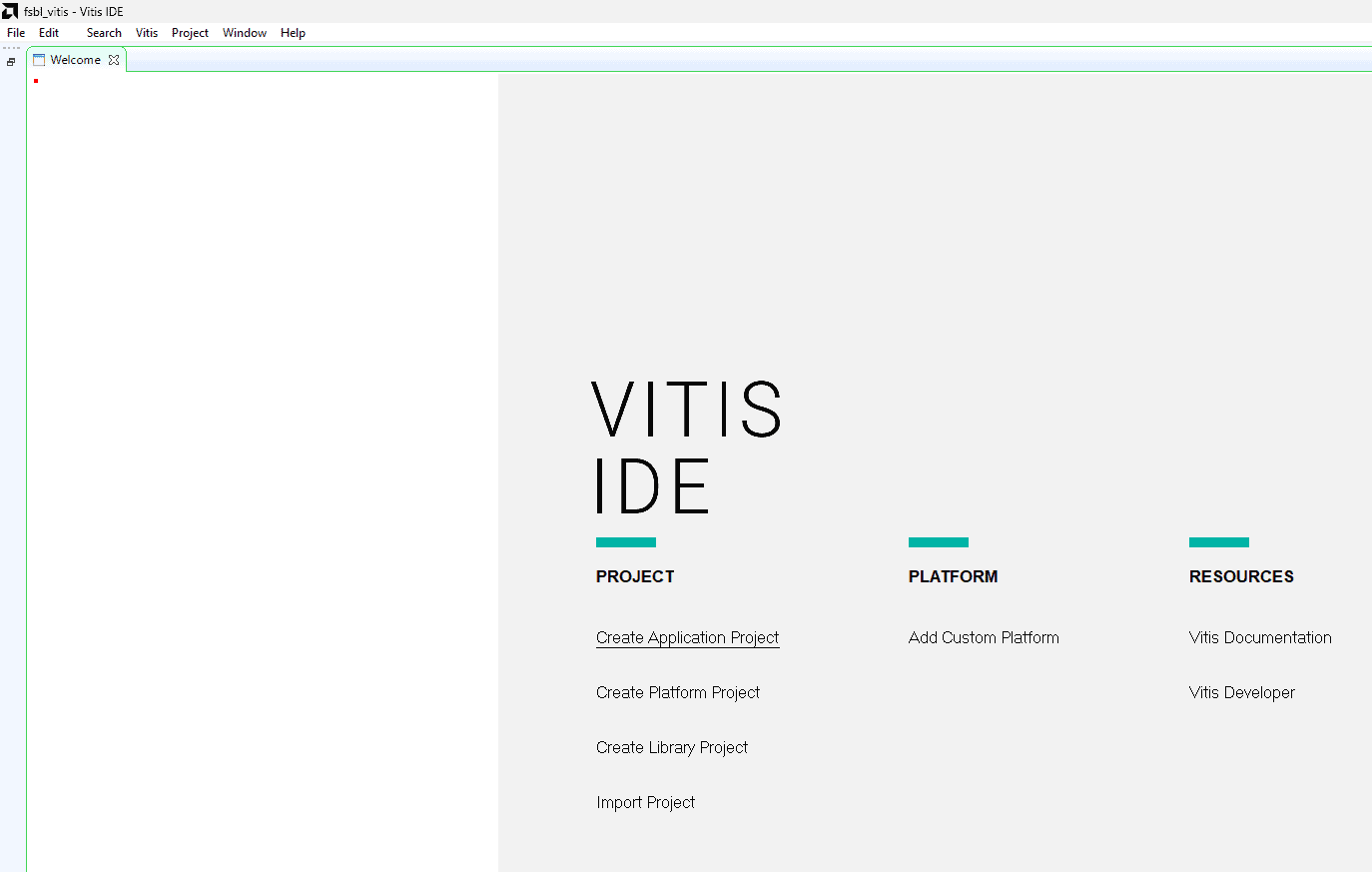
Step 17:
Once the Vitis window appears, select “Create Application Project”.
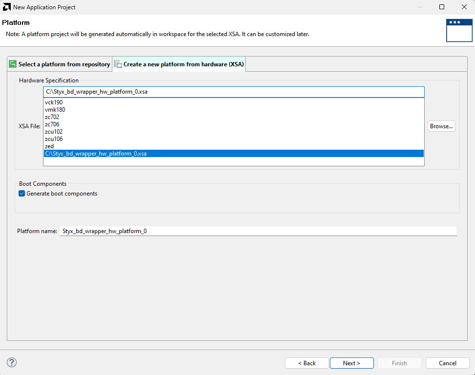
In the “Platform” window, select “Create a new platform from hardware” tab and import the “XSA file” which is already created (Provide XSA file location). click “Next”
Step 18:
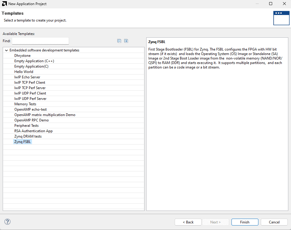
Now select the Zynq FSBL template from the list of available templates and click Finish.
Once the project is created, vitis will automatically run a build. If that didn’t happen for any reason, run a build manually.
Step 19:
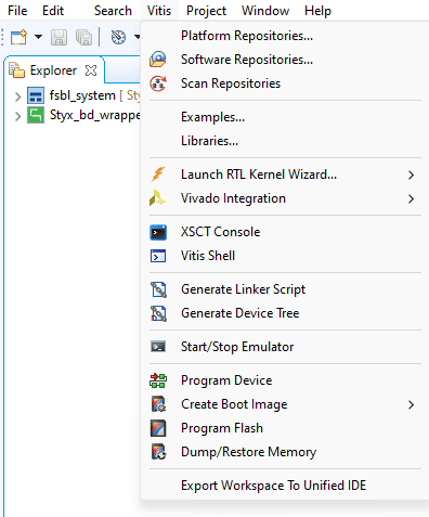
To create a bootable image and BIN file, go to Vitis -> Create Boot Image
Step 20:
In the create boot image window, provide a path for the Output BIF file and select Output format as BIN. Add the following files manually in boot image partitions,
- fsbl.elf (Bootloader)
- styx_bd_wrapper.bit (Bitstream)
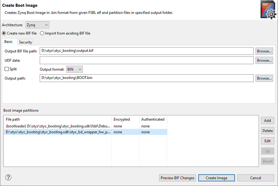
Click on Create Image.
Step 21:
Booting from QSPI Flash
For programing the Styx Board, use Tenagra FPGA Management software, refer “Getting started with Tenagra FPGA System Management Software” article.
Program the flash with the created BIN file and will be able to observe the output.
Booting from SD card
After generating the bin file successfully, copy the bin file into the SD card. Change the Styx boot mode to SD Card by following instructions in the Styx User Manual. Insert the SD card into Styx and connect the micro USB cable. Power up the board to observe the output.