Introduction
The Vivado Design Suite from Xilinx is used for the synthesis and analysis of HDL designs for Xilinx FPGAs with additional features for SoC development and high-level synthesis. This tool increases the overall productivity for designing, integrating and implementing systems with Xilinx’s UltraScale, 7 series devices, and Zynq-7000. In this article, we’ll be using the Vivado IP Integrator alongside the Vitis to create the classic “Hello World” project for the Tagus – Artix 7 PCI Express Development Board containing a 32-bit MicroBlaze soft processor and peripherals connected together by the AXI4 bus.
MicroBlaze is a 32-bit soft processor IP developed by Xilinx for their mid and high-end FPGA devices. It is compatible with Xilinx’s 6 and 7 series FPGAs. More information on Microblaze can be found at Xilinx’s MicroBlaze page. Advanced knowledge of MicroBlaze or AXI is not a prerequisite to follow this article. Thanks to the excellent tools provided by Xilinx, most of the design can be done without writing any code at all.
Tagus – Artix 7 PCI Express Development Board
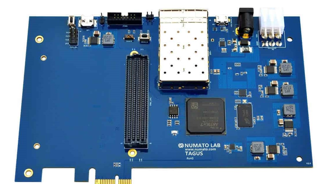
The Tagus is an FPGA Development Board from Numato Lab featuring the Xilinx’s Artix 7 FPGA with x1 PCI Express Interface. It also features a high-speed FMC connector enabling the users to add additional features to the board using FMC custom daughter boards. Thus the Tagus is a great choice for both learning and for high-end applications.
Prerequisites:
Hardware:
- Tagus – Artix 7 PCI Express Development Board.
- Xilinx Platform Cable USB II JTAG debugger.
- DC Power Supply (+12V recommended).
- USB A to Micro USB Cable.
Software:
- Vivado Design Suite with Vitis (2023.2.1 used).
- Serial terminal application (PuTTY, Tera Term, etc.).
Creating MicroBlaze based Hardware Platform for the Tagus
Before starting with the creation of the design, download and install Board Support Package (BSP) files for the Tagus – Artix 7 PCI Express Development Board from here (follow README.md for instructions on installation of BSP files).
Step 1: Creating a New Project
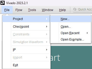
Launch the Vivado Design Suite, go to “File -> Project -> New” to create a new project. The “New project” wizard will pop up. Click “Next” to continue.
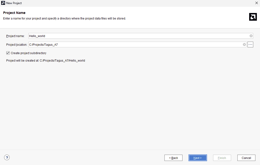
In the “Project Name” wizard, enter a name (for example, “tagus_microblaze“) for the project and save it at a convenient location. Select the checkbox below to keep all project files in a single folder. Click “Next” to proceed.
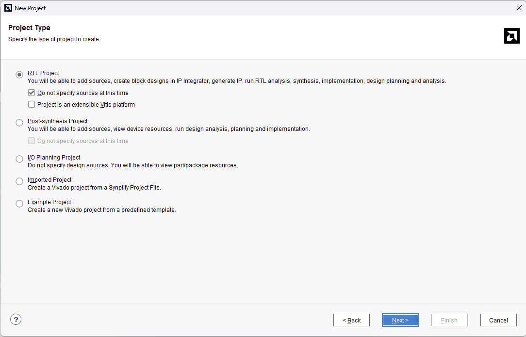
In the “Project type” wizard, select “RTL Project” and select the checkbox to skip specifying the sources at this moment. Click “Next”.
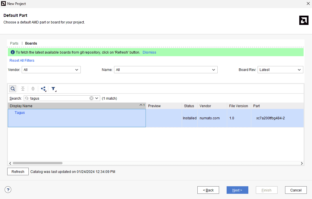
At the “Default Part” step, select “Boards” tab and then select the “Tagus” board. Click “Next” to continue.
In the next wizard, click “Finish” to create a new project.
Step 2: Creating Block Design
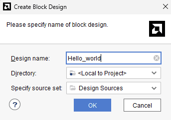
In the “Flow Navigator” panel, select “Create Block Design” under the IP integrator section. Give an appropriate name (Eg: “Hello_world”) to the design and click “OK”.
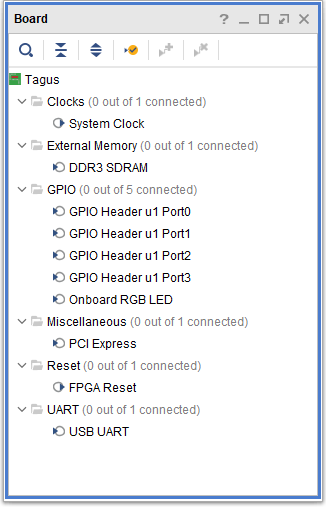
In the “Board” tab, we can observe the default peripherals available for the Tagus board. Drag and drop System Clock, DDR3 SDRAM and USB UART peripherals into the design.
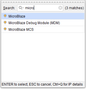
In the Diagram window, right-click and select “Add IP” from the popup menu. Search for “MicroBlaze” and add it to the design by double-clicking.
Double click “Clocking Wizard” IP and customize the “Output Clocks” settings as shown in the following image.
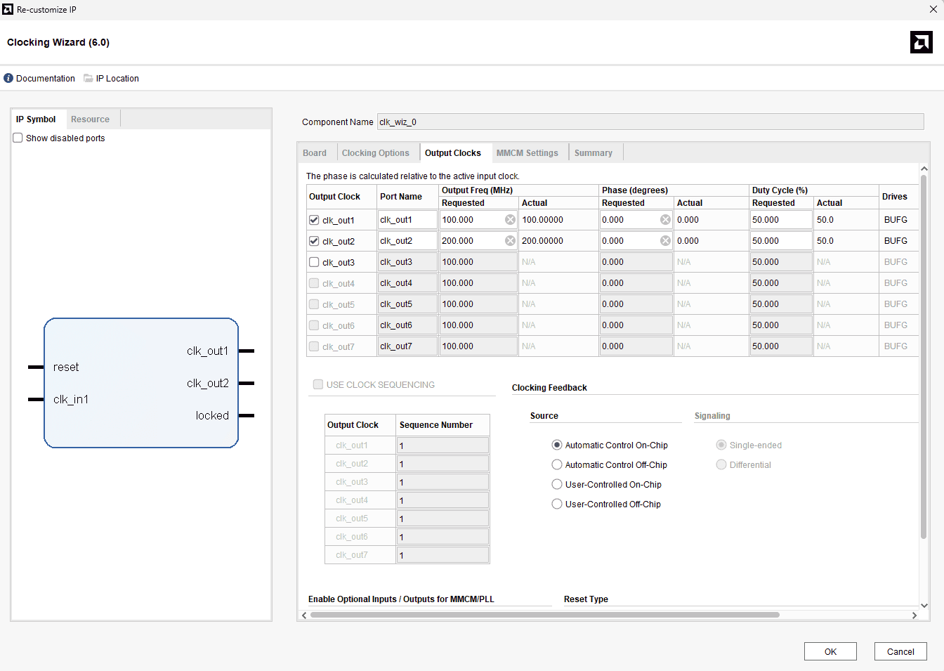
Remove the existing “sys_clk_i” connection and input port (if any) and connect the “clk_out2” net on the clocking Wizard to “sys_clk_i” of “MIG 7 Series” block as shown in the following image.
Step 3: Run Block Automation, Run Connection Automation & Validate Design
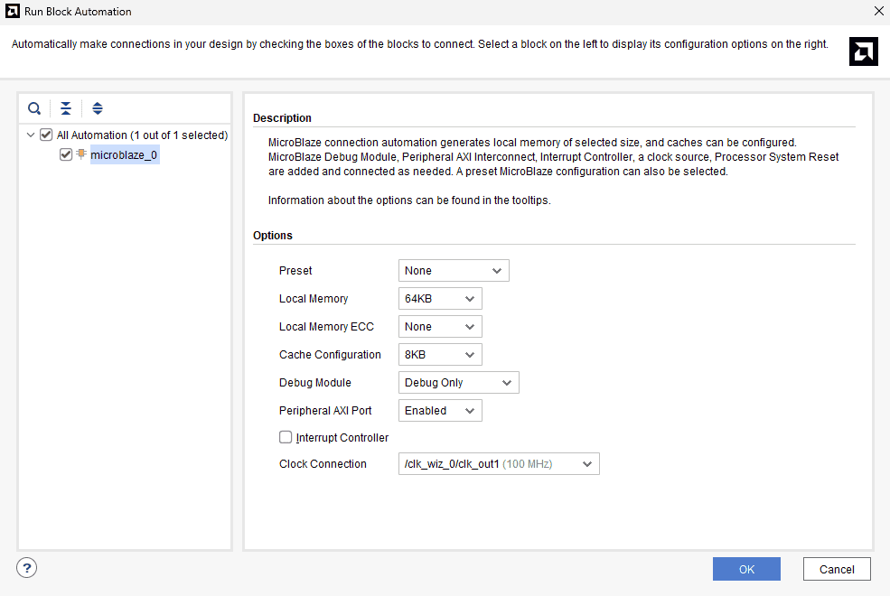
Click “Run Block Automation” present in the “Designer Assistance available” bar on the top-left corner of the window to complete the design. Select the settings as shown in the following image. Click “OK” for the Vivado to automatically configure the blocks for us.
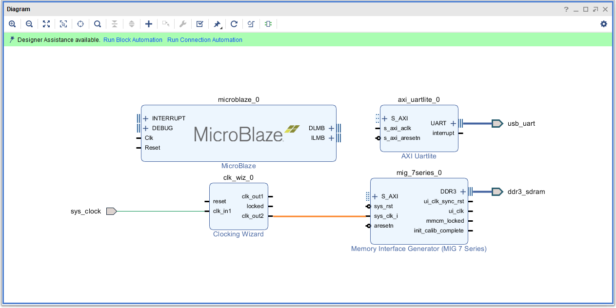
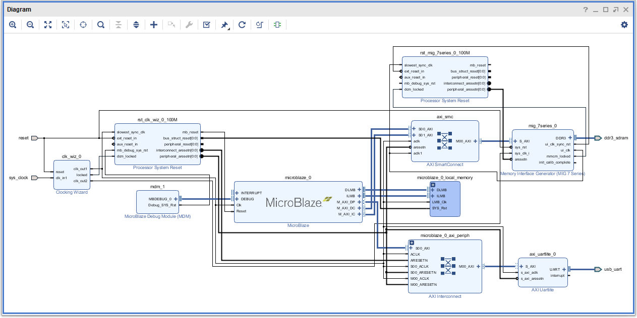
Once the Block Automation is complete, select “Run Connection Automation” so Vivado can connect the blocks together to make a complete system. Select the “Validate Design” option from the Tools menu to make sure that the connections are correct and save the design. The final design will look similar to the image below.
Step 4: Create HDL Wrapper and Generate Bitstream
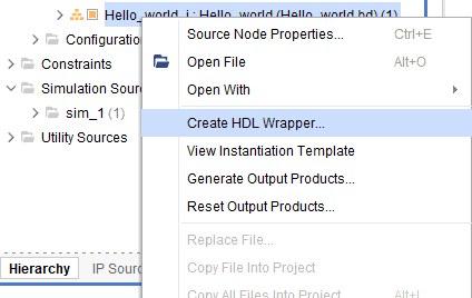
Right-click “Hello_world” in the “Sources” window, select the “Create HDL Wrapper” option from the popup menu. Click “OK” on the window that appears to finish generating a wrapper.
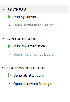
Click “Generate Bitstream” under the “Program And Debug” section to synthesize, implement and generate a bitstream.
Step 5: Export Hardware and Launch Vitis
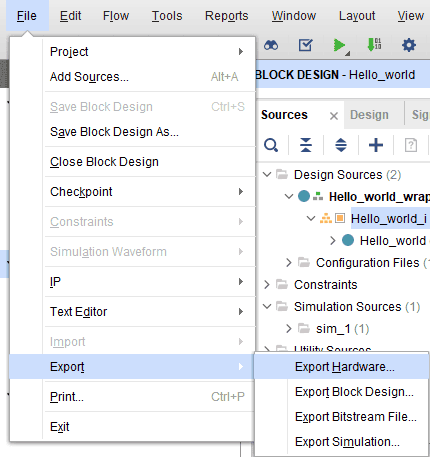
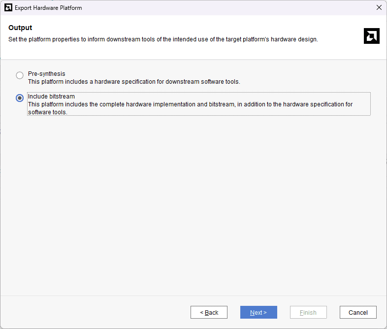
Once the implementation and generation of the bitstream are successfully completed, we need to export the hardware along with the bitstream. Go to the “File” menu, select “Export -> Export Hardware”. Select the “Include bitstream” checkbox and click “OK” in the “Export Hardware” wizard.
Software Development in Vitis For Tagus
Step 1:
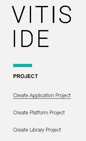
Launch Vitis IDE. In the Vitis window, select “Create Application Project” and click “Next” in the dialog box that appears.
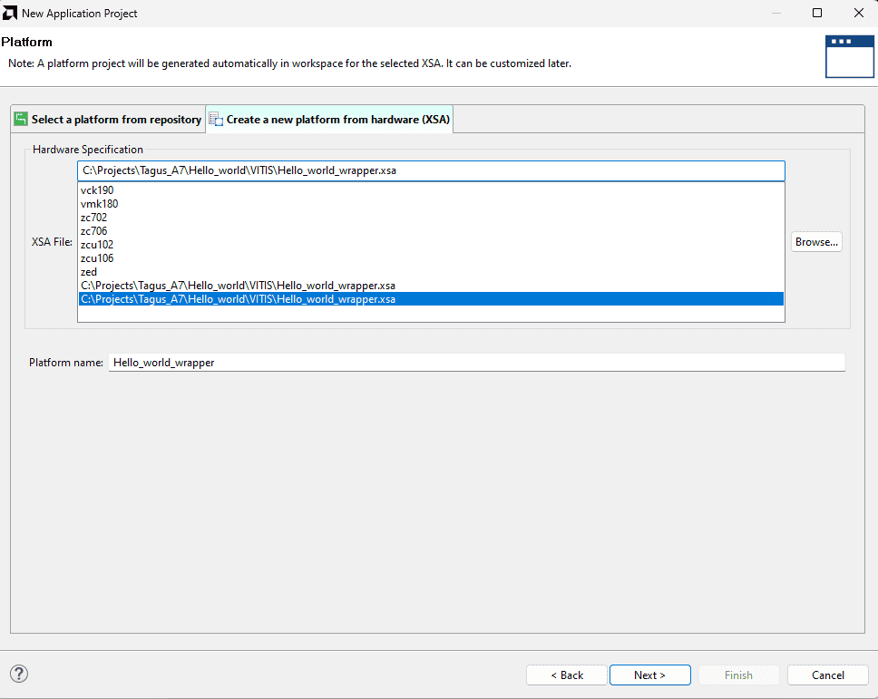
In the “Platform” window, select “Create a new platform from hardware” tab and import the “XSA file” which is already created (Provide XSA file location). Click “Next“
Step 2:
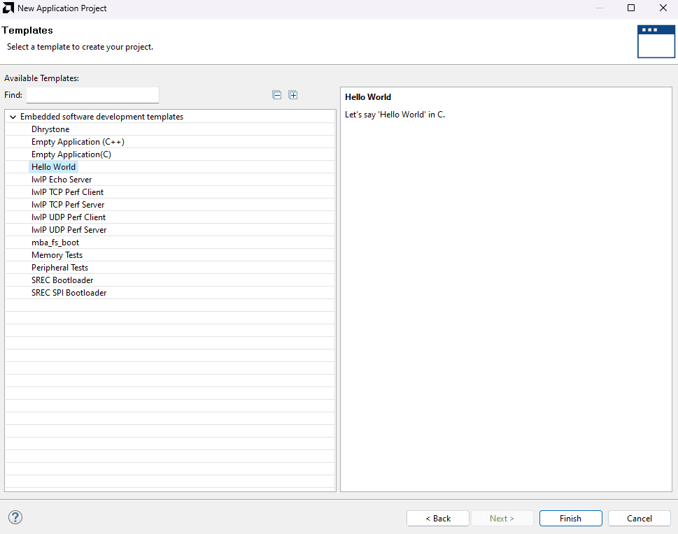
In the “Application Project Details” window, give an appropriate name for the Vitis Project and click “Next“. Click “Next” in the “Domain” window. Select the “Hello World” template from the list of available templates and click “Finish“.
Step 3:
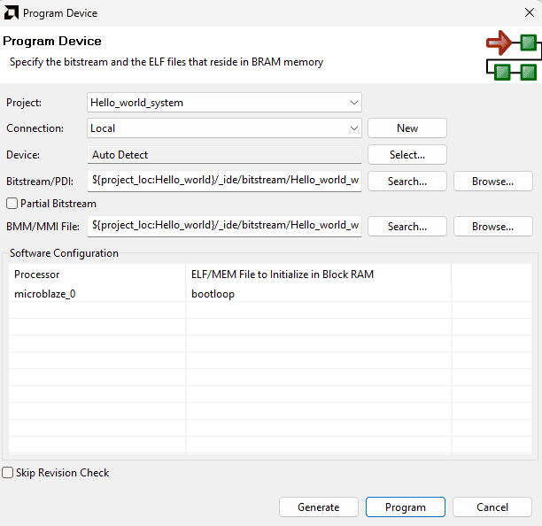
Build the project. Once the build is completed successfully, power up the Tagus – Artix 7 PCI Express Development Board using external DC power supply, and connect the Xilinx Platform USB JTAG cable and the USB Micro Type-B cable to the board. Program the FPGA on Tagus with a simple boot loop program by selecting the “Program Device” option from the “Vitis” menu.
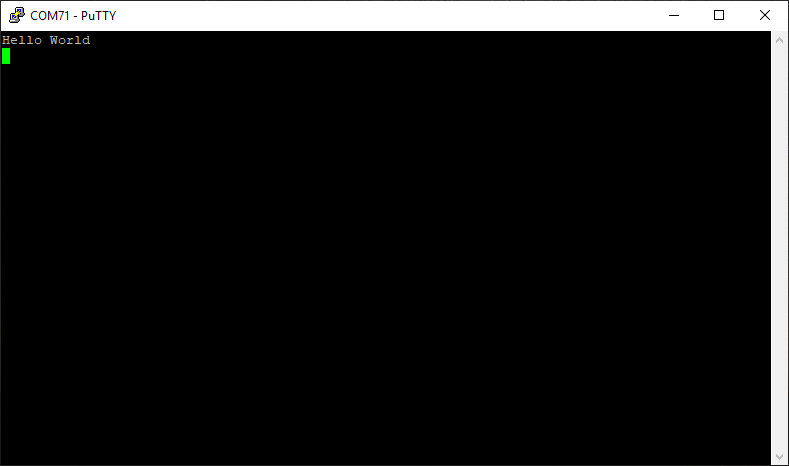
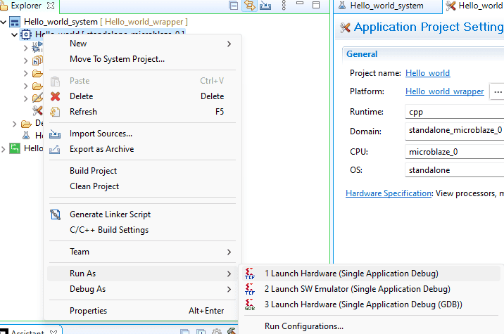
Open the COM port corresponding to Tagus_A7 in any serial terminal (PuTTY, Tera Term, etc.) with a 9600 baud rate (the default baud rate given in UART IP). Now, right-click on the “.elf file” in Project Explorer and select “Launch Hardware” as shown below.
If everything went well, the application running on the board should print “Hello World” over the USB UART and should be displayed on the Serial Terminal application.