Introduction
The Vivado Design Suite from Xilinx is used for the synthesis and analysis of HDL designs for Xilinx FPGAs, superseding the Xilinx ISE Design Suite with additional features for SoC development and high-level synthesis. This tool increases the overall productivity for designing, integrating and implementing systems with Xilinx’s UltraScale, 7 series devices, and Zynq-7000. In this article, we’ll be using the Vivado IP Integrator alongside the Vivado SDK to create the classic “Hello World” project for the Aller Artix-7 FPGA Board containing a 32-bit MicroBlaze soft processor and peripherals connected by the AXI4 bus.
What is MicroBlaze?
MicroBlaze is a 32-bit soft processor IP developed by Xilinx for their mid and high-end FPGA devices. It is compatible with Xilinx’s 6 and 7 series FPGAs. More information on MicroBlaze can be found on Xilinx’s MicroBlaze page. Advanced knowledge of MicroBlaze or AXI is not a prerequisite to follow this article. Thanks to the excellent tools provided by Xilinx, most of the design can be done without writing any code at all.
What is AXI?
AXI stands for Advanced eXtensible Interface. AXI is a bus interconnect based on ARM’s popular AMBA bus architecture. In a MicroBlaze system, AXI connects the microprocessor to all peripherals in the system. The only exception is the Block RAM which is attached to the processor through the LMB (Local Memory Bus). AXI4-Lite is available for connecting low throughput peripherals to the system such as the UART, GPIO, etc. AXI4-Lite uses fewer logic resources on FPGA compared to AXI. Usually, AXI is used to connect high throughput peripherals such as DDR memory, Ethernet, etc. Again, a detailed understanding of AXI is not required for following this article. But for curious readers, AXI Reference Guide is available here.
Aller Artix-7 FPGA Board with M.2 Interface
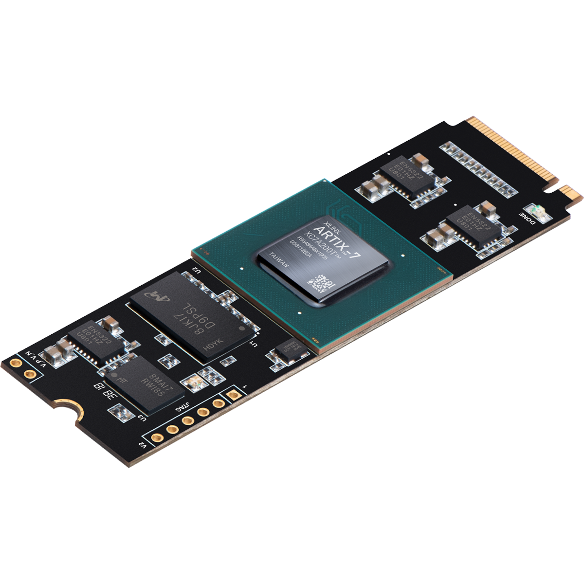
The Aller board from Numato Lab is an Artix-7 based development board designed to ease accelerated computing. It features an M.2 form factor M-key slot which is a computer storage interface based on the PCI Express standard. Thus Aller can be used with laptops, desktops, and servers seamlessly through its M.2 interface. This article will serve as a quick start guide for you to get familiar with Aller. Let’s get started!
Prerequisites:
Hardware:
- Aller Artix-7 FPGA Board with M.2 Interface
- Xilinx Platform Cable USB II
Software:
- Vivado Design Suite with SDK installed (2018.2 or higher)
Creating MicroBlaze based Hardware Platform for Aller
The following steps will walk you through the process of creating a new project with Vivado and building a hardware platform with a MicroBlaze soft processor using the Vivado IP integrator. Screenshots are added wherever possible to make the process easier for the reader.
Step 1:
Download and install the Vivado Board Support Package files for Aller from here. Follow the README.md file on how to install Vivado board support files for Numato Lab boards.
Step 2:
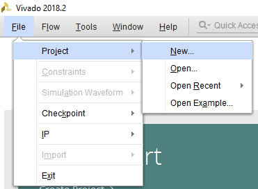
Open the Xilinx Vivado Design suite, go to “File->Project ->New” to create a new project. The “New project” window will pop up. Click “Next”.
Step 3:
In the “Project Name” window, enter a name for the project and save it at a suitable location. Select the option “Create project subdirectory” to keep all the project files in a single folder.
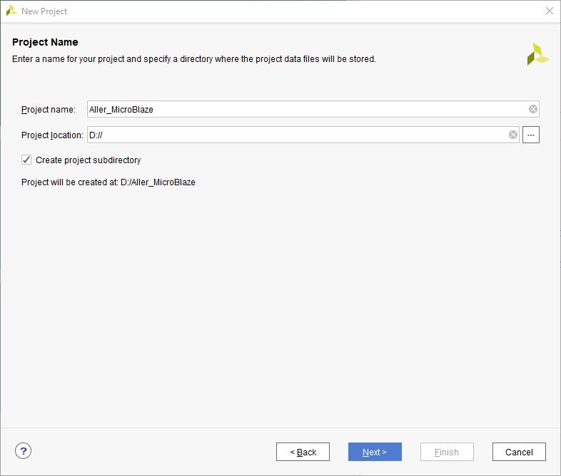
For this example, “Aller_MicroBlaze” is used as the project name, but feel free to use any name. Click “Next” without making any changes until you see the “Default Part” page.
Step 4:
In the “Default Part” window, select the “Boards” tab. Choose the Vendor as “numato.com”, filter the Name “Aller_200T” and select the board as shown below. If Aller is not displayed in the Boards list, make sure that the board support files are installed correctly.
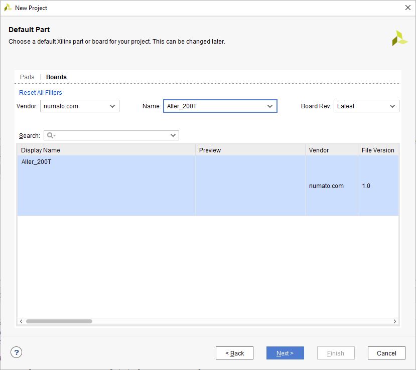
Click “Next” to continue. On the next page, click “Finish” to complete creating a new project. A new project will be created by Vivado with the selected settings.
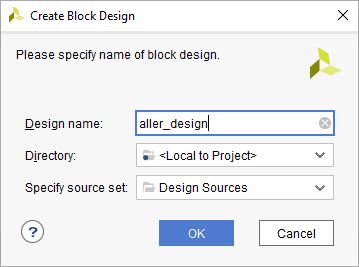
Step 5:
Under the “Flow Navigator” panel, click “Create Block Design” under the IP Integrator section. Enter a name for the block design and click “OK”.
An empty block design will be created.
Step 6:
As shown in the “Diagram” window, click the “Add IP” icon, search for MicroBlaze and add it to the design by double-clicking its name in the list.
![]()
Similarly, add AXI Timer to the block design.
Step 7:
Click the “Board” tab. The default peripherals available for the Aller board will be listed as shown below.
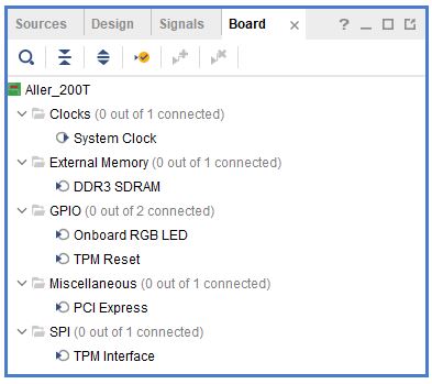
Drag and drop the System Clock and DDR3 SDRAM peripherals into the block design. Remove the existing connection to sys_clk_i the “MIG 7 Series” block.
Step 8:
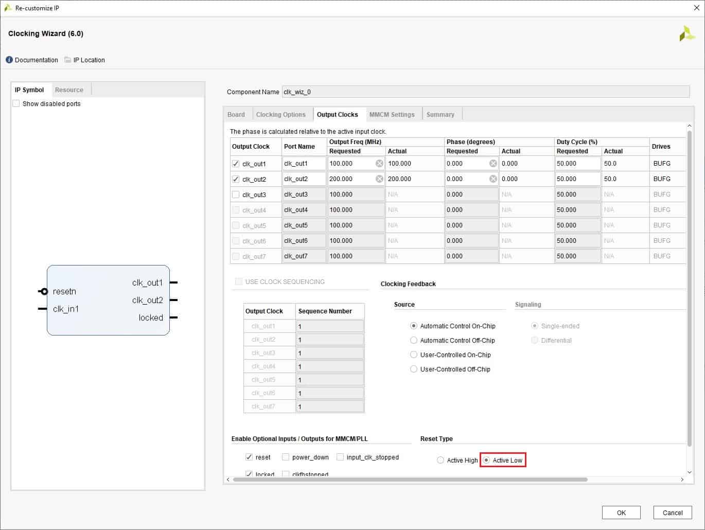
Double-click on the “Clocking Wizard” IP block and change the settings as shown below. In the “Output Clocks” section, set clk_out1 frequency to 100 MHz and clk_out2 frequency to 200 MHz. Set “Reset Type” Active Low and click “OK” to customize the IP.
Step 9:
Click “Run Block Automation” and change the settings as shown below. Enable “Debug & UART” in the Debug Module to use JTAG UART of the MicroBlaze Debug Module (MDM). We will use JTAG UART since Aller does not have an onboard USB interface. Also, enable the “Interrupt Controller” checkbox.
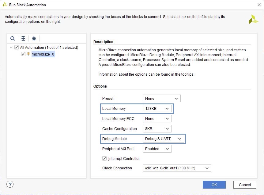
Click “OK” for Vivado to automatically configure the blocks for you.
Step 10:
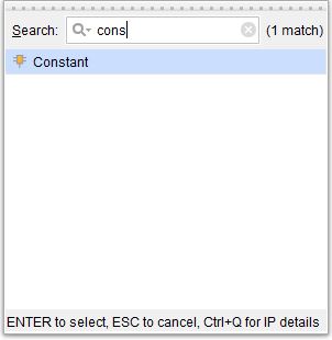
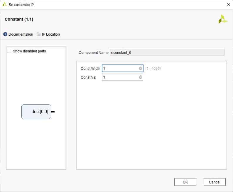
Press the “Add IP” icon and search for Constant block as shown in the image below. Drag and drop it to the Diagram window.
Double-click on the Constant block and confirm that its settings are as follows.
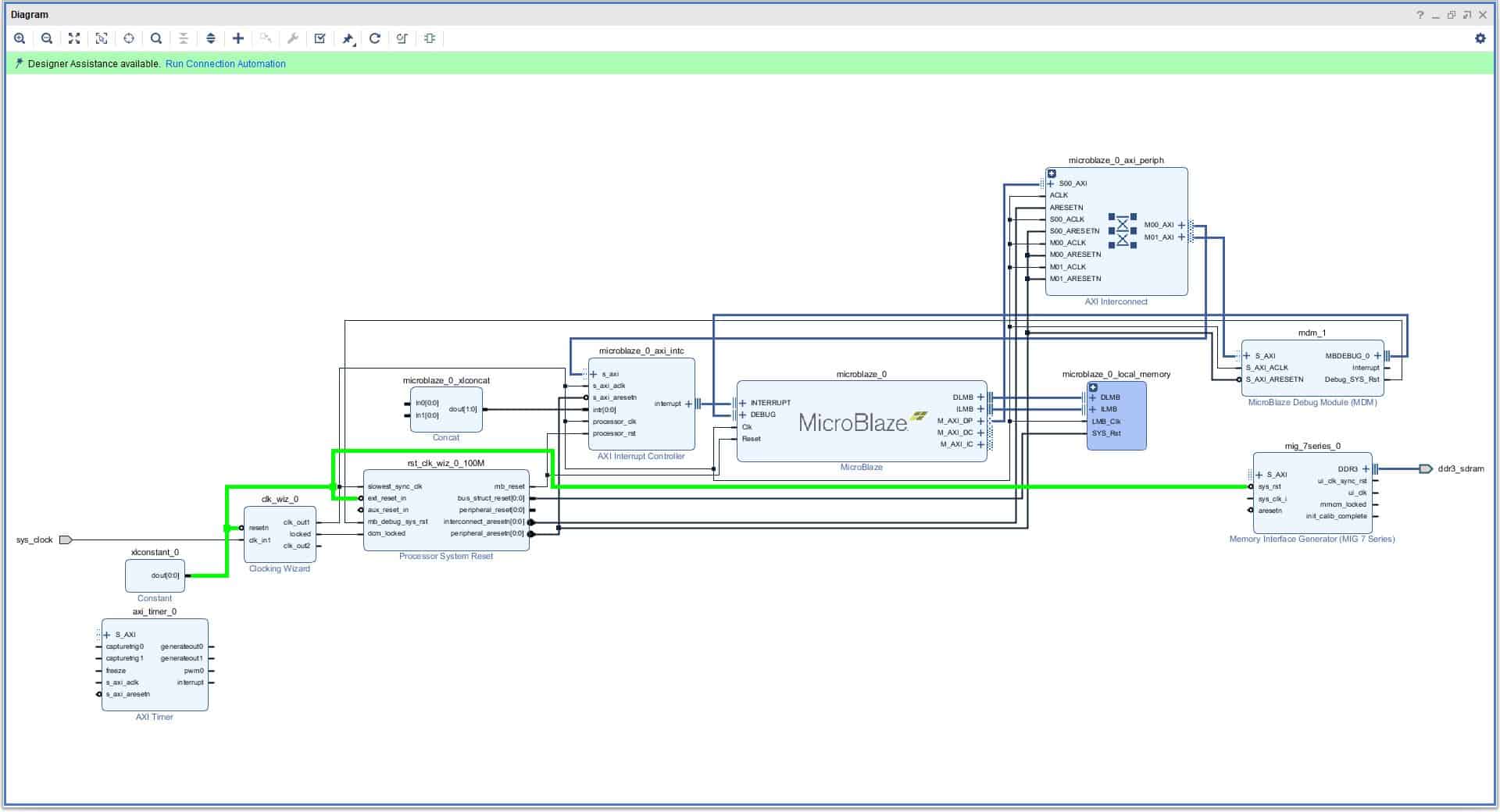
Now, connect the output of this block to resetn of “Clocking Wizard”, ext_reset_in of the “Processor System Reset” and sys_rst of the “MIG 7 Series” block. These connections are highlighted in green in the following image.
Step 11:
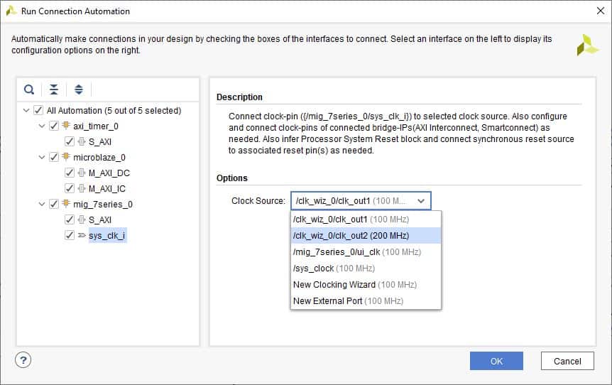
Click “Run Connection Automation” and select the “All Automation” checkbox as shown in the image below. Now, select sys_clk_i under “mig_7series_0” and choose the “Clock Source” as clk_out2 the output of the Clocking Wizard. Click “OK”.
Vivado will now connect the blocks together to make a complete system.
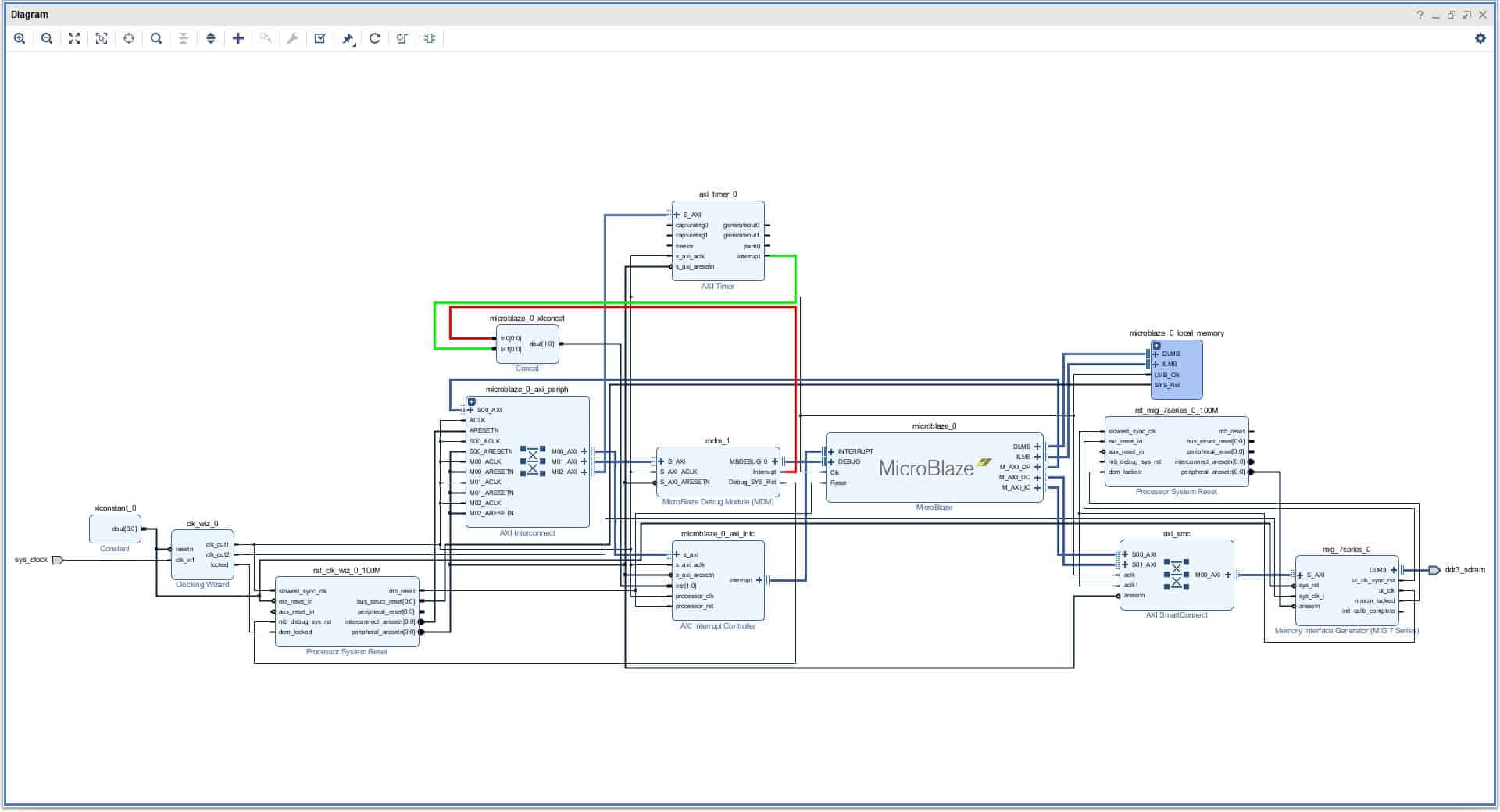
Step 12:
Connect the interrupts from mdm_1 and axi_timer_0 to the Concat block as shown below (the order does not matter). Make sure that the final design looks similar to the image below.
Step 13:
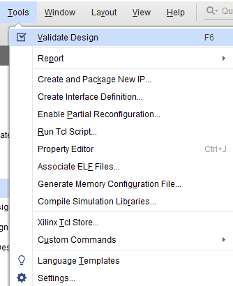
Select the “Validate Design” option from the Tools menu to ensure that the connections are correct.
Step 14:
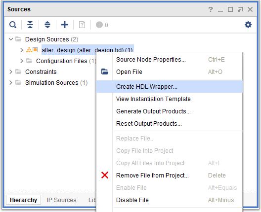
Save the design and then right-click on the block design in the “Sources” window, select the “Create HDL Wrapper” from the popup menu. Click “OK” on the window that appears to finish generating the wrapper.
Step 15:
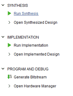
Select “Run Synthesis” followed by “Run Implementation”. If the design is implemented successfully, then select “Generate Bitstream”.
Step 16:
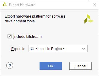
If the bitstream is generated successfully, we can export the hardware platform along with the bitstream to the Xilinx SDK. Go to “File -> Export -> Export Hardware”, and select the “Include bitstream” checkbox in the window that pops up.
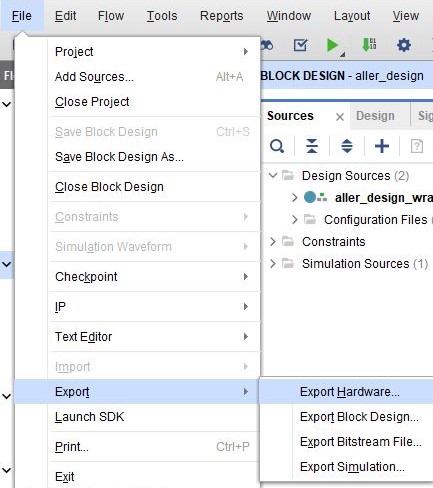
You may select “<Local to Project>” to export the files to the local project directory or choose another directory, and click “OK”.
Step 17:
Select “Launch SDK” from the File menu. In the window that appears, select the location where the hardware platform was exported as the “Exported location” and select the SDK workspace as well.
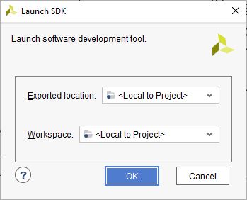
Click “OK” to launch the Xilinx SDK.
In the next section, we will see how to create a basic “Hello World” project using the Xilinx SDK.
Software Development in SDK
The SDK launches and a hardware platform project for the design will be automatically created. The hardware platform specification project will be displayed in the Project Explorer of SDK.
Step 1:
Go to File -> New -> Application Project. In the window that follows, enter a project name, select the hardware platform and click “Next”.
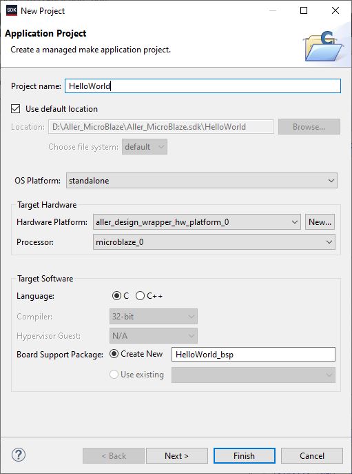
On the next page, select “Hello World” from the list of available templates and click “Finish”.
Step 2:
Once the project is created, the SDK will automatically run a build. If that didn’t happen for any reason, run the build manually. Once the build is completed successfully, power up the Aller and connect the Xilinx Platform USB II JTAG cable to the board.
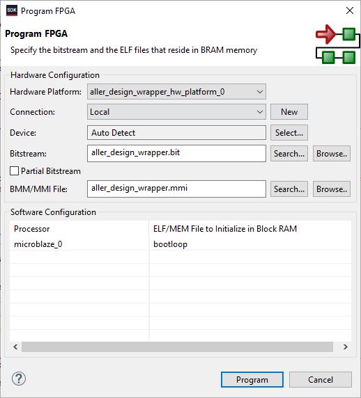
Step 3:
Program the FPGA on Aller with the generated bitstream and simple bootloop firmware by selecting the “Program FPGA” option from the “Xilinx” menu in SDK Window.
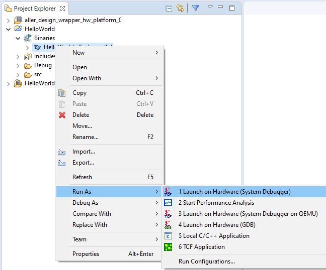
Step 4:
Right-click on the .elf file in the Project Explorer and select “Launch on Hardware” as shown below.
If everything went well, the Hello World application running on the board should print “Hello World” over the JTAG UART and the output should be displayed in the SDK’s console terminal as shown in the image below.
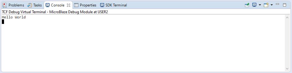
Congratulations on getting your first design running successfully on Aller!