Introduction
The TityraCore Waveform Viewer is a powerful demonstration and development framework designed to showcase the full capabilities of the TityraCore Zynq 7000 FPGA Development Board. This project transforms the embedded platform into a fully functional, real-time, Web-Enabled Data Acquisition and Control System, accessible via any standard web browser.
This solution serves as a crucial bridge, allowing users to move beyond traditional embedded debugging and immediately interact with the Zynq’s integrated hardware resources over a standard Ethernet connection.
Core Project Features
This framework leverages the Zynq’s dual-core ARM Processing System (PS) and Programmable Logic (PL) to implement the following key features, all integrated into a single, cohesive web interface:
- 🌐 Embedded Web Server: A robust LwIP-based HTTP server hosts a dynamic, mobile-friendly interface for seamless remote interaction and monitoring.
- 📈 Live Digital Input Waveform Acquisition: The core feature utilizes the Processing System (PS) to achieve precise, high-frequency data sampling from the PL-side AXI GPIO. This raw digital input is streamed to the browser via JSON and rendered as a live, scrolling waveform using the Chart.js library, effectively turning the Zynq into a remote oscilloscope.
- 🌡️ Real-Time Sensor Monitoring (XADC): The project continuously samples and displays environmental and operational health data from the on-chip XADC (Analog-to-Digital Converter), including internal die temperature and core voltages. This ensures developers can monitor the FPGA’s status during demanding operations.
- 💡 Remote Hardware Control (GPIO): Demonstrates full bidirectional control by allowing users to toggle an external LED (or similar peripheral) via an HTTP POST request, confirming robust command-and-control capability over the hardware I/O.
- 🔗 Optimized Architecture: The high-speed network polling and the critical data acquisition (waveform sampling) are implemented using an optimized interrupt-driven architecture, ensuring deterministic, low-jitter sampling while maintaining network responsiveness.
Prerequisites:
- Hardware:
- TityraCore FPGA Development Board
- Cat 6 Ethernet Cable
- USB Type C Cable.
- 5V&12V DC Power Supply
- Numato AD9283 ADC Expansion Module
- Function Generator
- BNC to SMA cable
- Software:
- AMD Vivado Design Suite 2025.1 or higher
- AMD Vitis Classic 2024.1
- Serial Terminal (PuTTY, Tera Term, etc.)
Let’s get Started
The following steps will walk you through the process of creating a new project with Vivado and building a hardware platform with Zynq processing system using IP integrator. This article is written for Numato Lab’s Tityra core D200 Module, but can be adapted to any other Zynq based platform with minor changes. Screenshots are added wherever possible to make the process easier to the reader.
Step 1:
Start Vivado Design Suite, and select “Create New Project” from Quick Start section. The project wizard will pop up. Press next to proceed with creating the project.
Step 2:
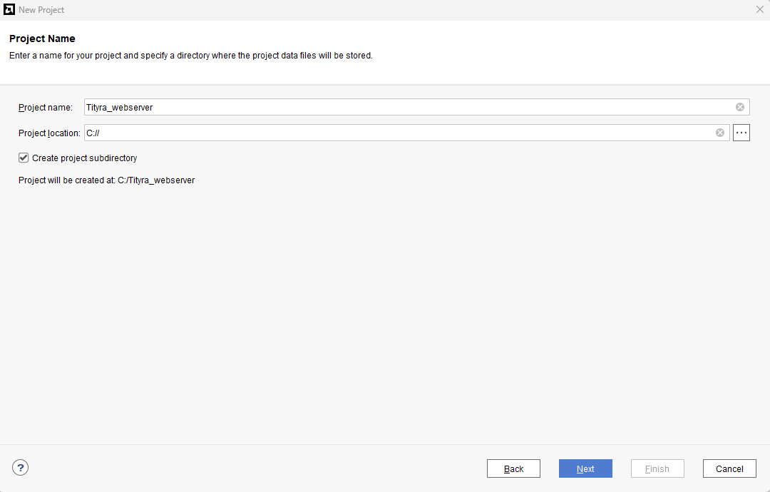
Type in a project name and save it at a convenient location. For this example “Ethernet_echo” is used as project name, but feel free to use any name. Select the check box below to keep all project files in a single folder. The image below shows the settings for the example project. Click “Next” to continue.
Step 3:
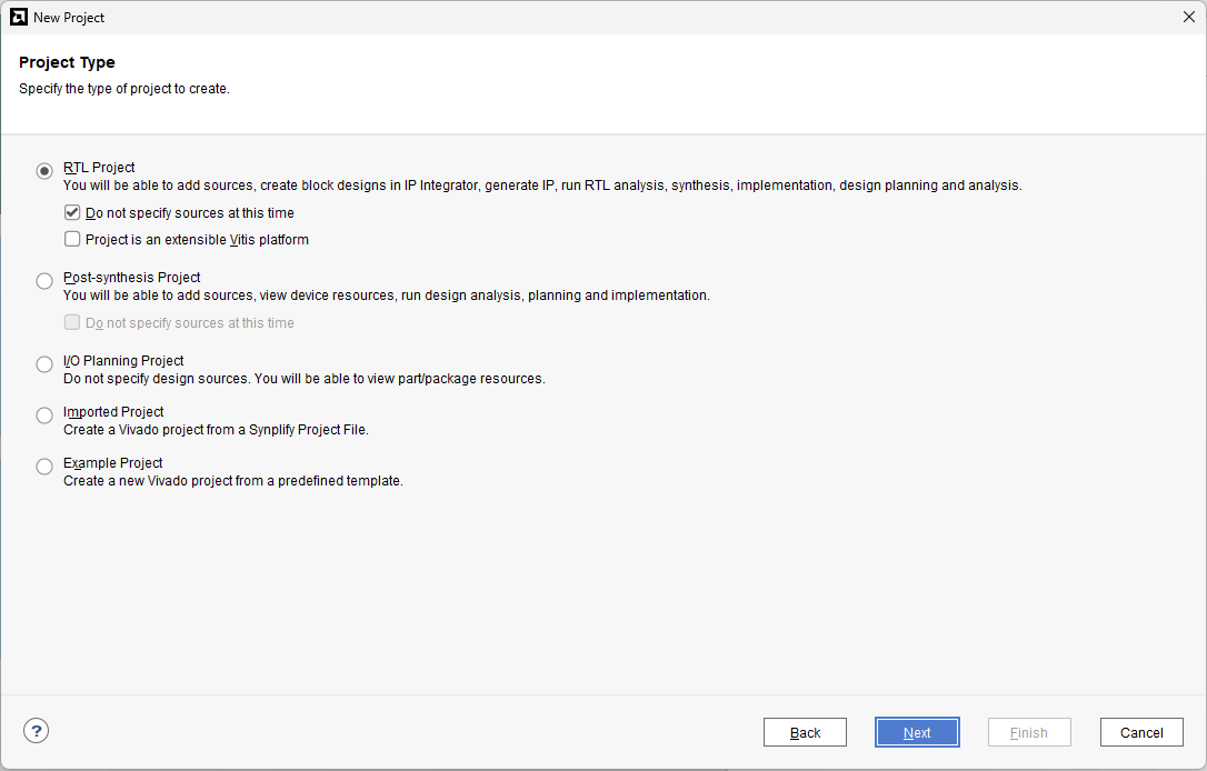
Choose “RTL Project” as project type and check the option “Do not specify sources at this time”.
Step 4:
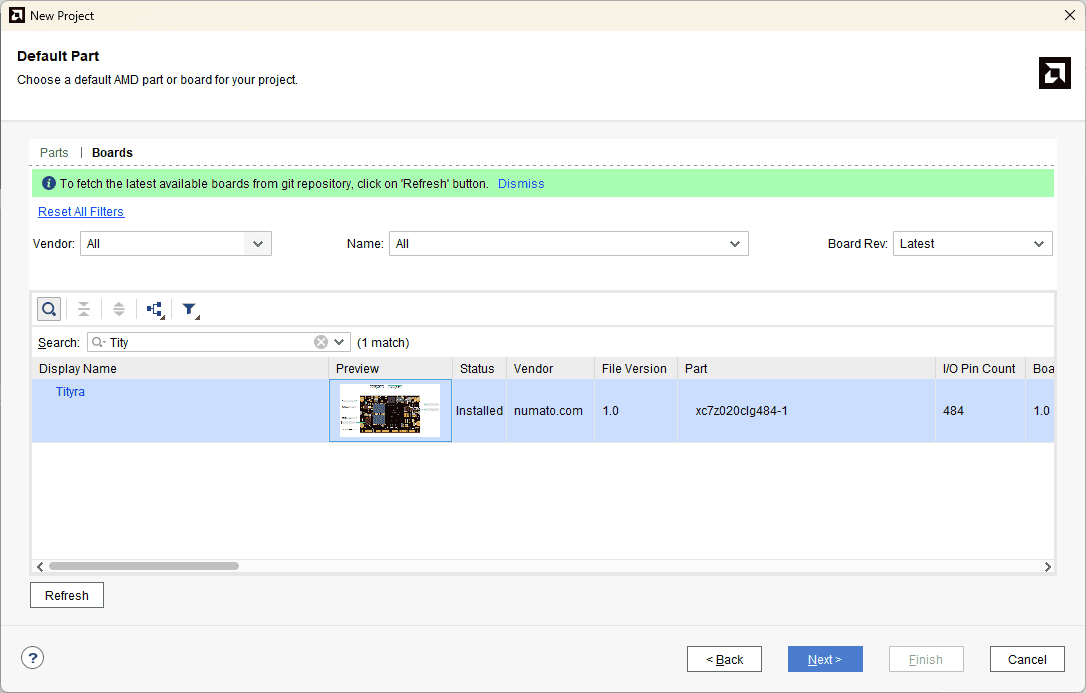
At the “Default Part” stage, switch to the “Boards” tab and set the vendor to numato.com. Select “Tityra” and click Next.If the Tityra board does not appear in the list, click “Refresh” to update the board catalog. Vivado will then download the latest board files, after which Tityra will become available for selection.
Step 5:
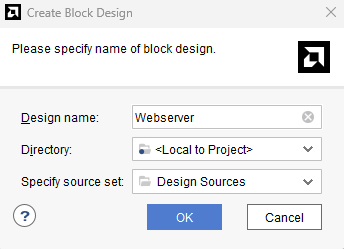
Under Flow Navigator, select “Create Block Design” in IP Integrator. Give an appropriate name to design. We will call it “Webserver” for example.
Step 6:
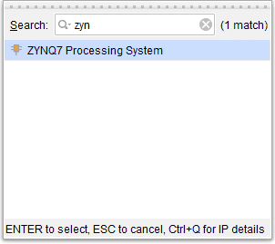
Go to Diagram window, right click and select “Add IP” from the popup menu. Search for ZYNQ7 Processing System. Add it to block design by double clicking.
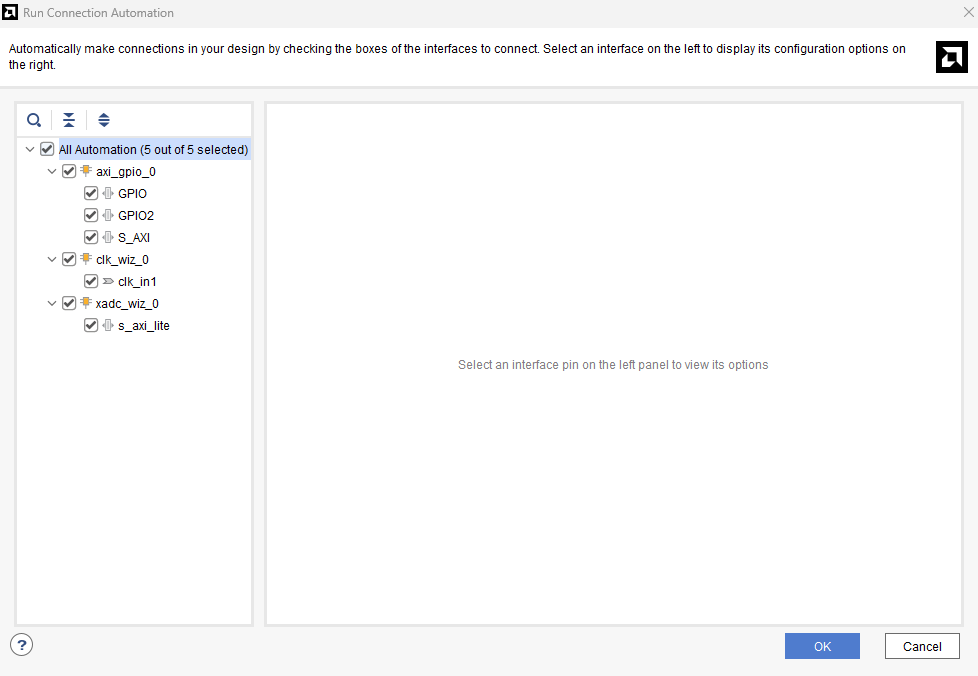
Step 7:
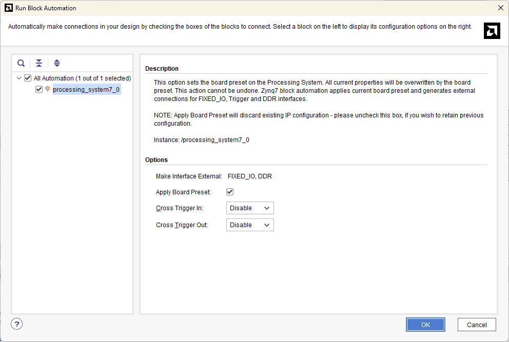
In the “Run Block Automation” window, select the options as in image below and click OK.
Step 8:
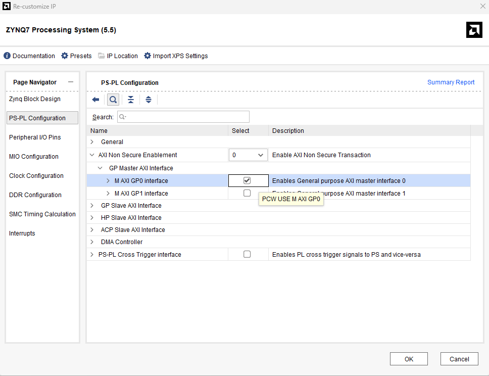
After running “Block Automation”, double-click the ZYNQ7 Processing System block to open the customization window.
Navigate to PS-PL Configuration, then open the AXI Non-Secure Enablement tab.
Enable the M AXI GP0 interface, and click OK to close the configuration window.
Step 9:
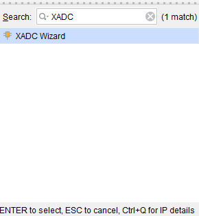
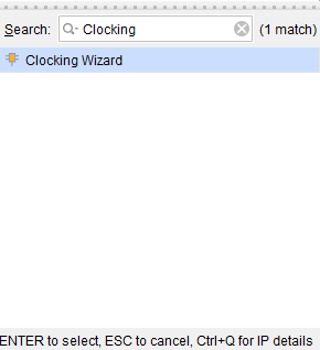
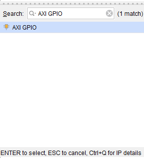
Go to Diagram window, right click and select “Add IP” from the popup menu. Add XADC WIZARD , AXI GPIO, Clocking wizard IP’s from the IP Catalogue .
Step 10:
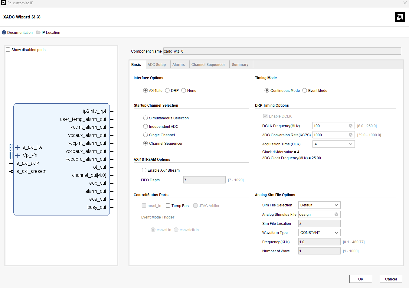
Double click on XADC Wizard IP to customize it , and in the ‘Basic’ tab select the ‘Startup channel Selection’ as ‘Channel Sequencer’.
In the ‘Channel Sequencer’ tab make the selections as in the picture below:
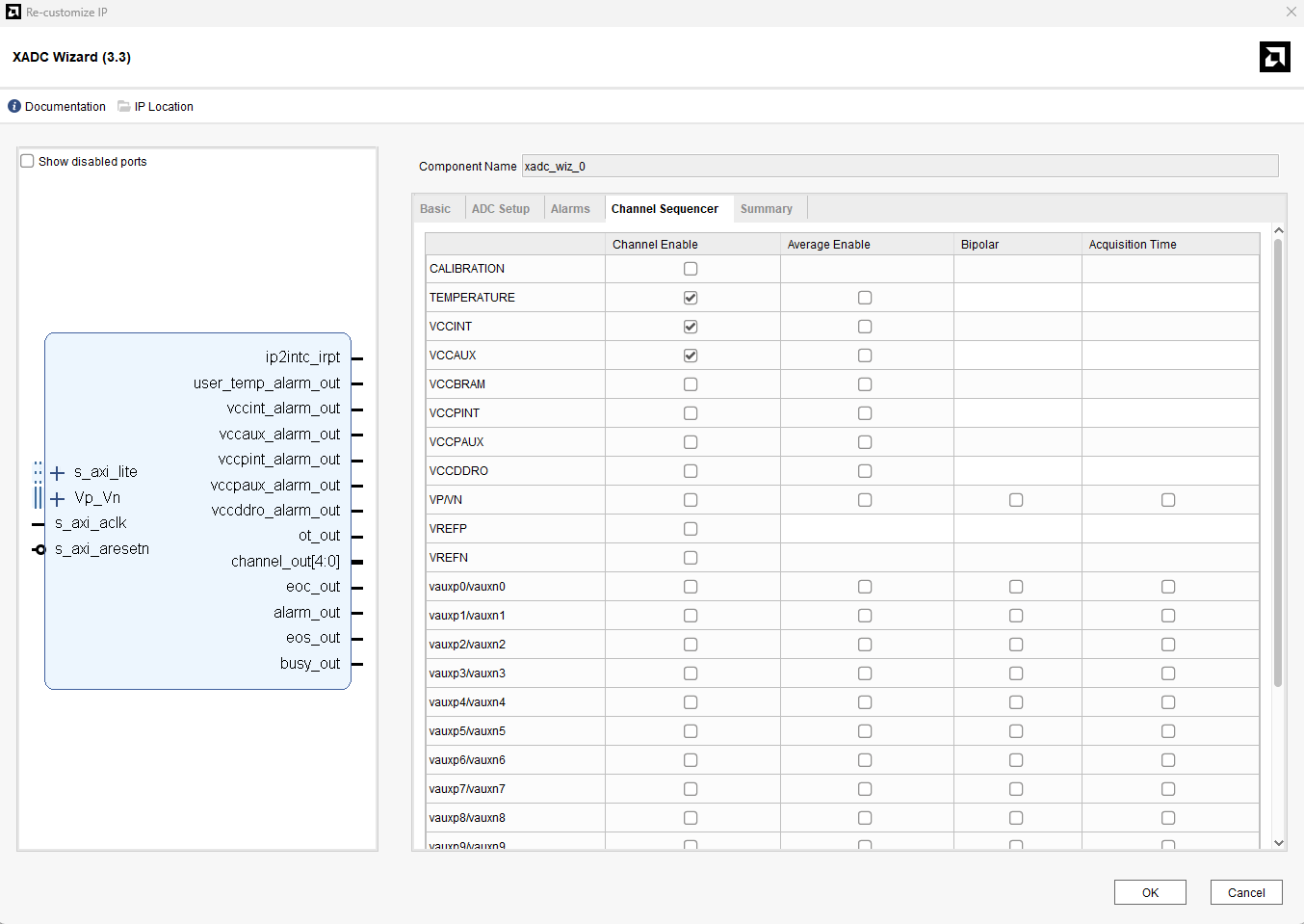
Click ok to finish the ip configuration.
Step 11:
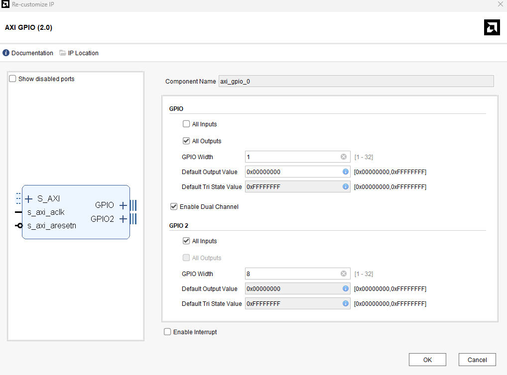
Next double click on AXI GPIO IP to customize it. Make the changes as per the image below.
Step 12:
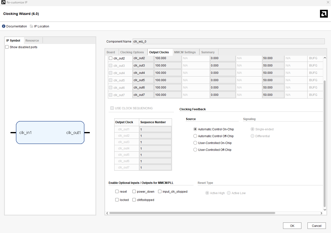
Next customize the clocking wizard IP by double clicking on the ip and disable the ‘reset’ and ‘locked’, and make sure the output clock is 100MHz ‘Output Clocks’ tab.
Step 13:
Run block automation
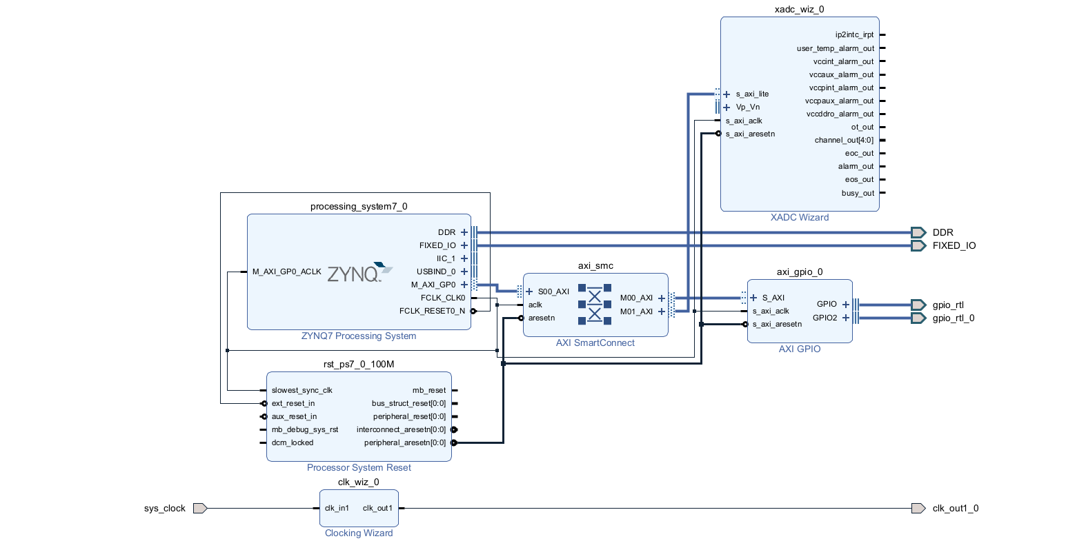
Step 14:
Next make the clocking wizards clk_out1_0 as external pin by right clicking on the ip and selecting ‘make external’ option, and make sure the final block diagram looks like the image below:
Step 15:
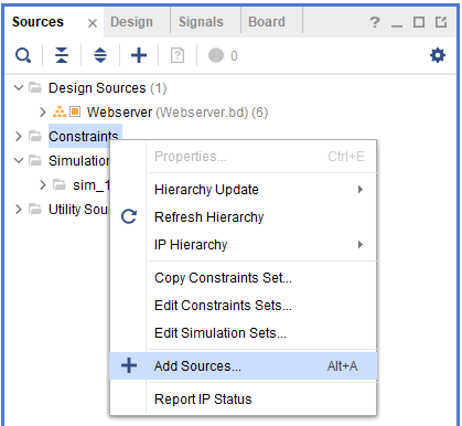
Right click on Constraints add select’Add Sources’ to add constraints.
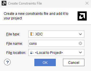
Create a constraints file and add the constraints given below to the newly created constraints file.
set_property IOSTANDARD LVCMOS33 [get_ports {gpio_rtl_tri_o[0]}]
set_property PACKAGE_PIN AB14 [get_ports {gpio_rtl_tri_o[0]}]
set_property IOSTANDARD LVCMOS33 [get_ports {gpio_rtl_0_tri_i[7]}]
set_property IOSTANDARD LVCMOS33 [get_ports {gpio_rtl_0_tri_i[6]}]
set_property IOSTANDARD LVCMOS33 [get_ports {gpio_rtl_0_tri_i[5]}]
set_property IOSTANDARD LVCMOS33 [get_ports {gpio_rtl_0_tri_i[4]}]
set_property IOSTANDARD LVCMOS33 [get_ports {gpio_rtl_0_tri_i[3]}]
set_property IOSTANDARD LVCMOS33 [get_ports {gpio_rtl_0_tri_i[2]}]
set_property IOSTANDARD LVCMOS33 [get_ports {gpio_rtl_0_tri_i[1]}]
set_property IOSTANDARD LVCMOS33 [get_ports {gpio_rtl_0_tri_i[0]}]
set_property PACKAGE_PIN AA22 [get_ports {gpio_rtl_0_tri_i[7]}]
set_property PACKAGE_PIN Y20 [get_ports {gpio_rtl_0_tri_i[6]}]
set_property PACKAGE_PIN U20 [get_ports {gpio_rtl_0_tri_i[5]}]
set_property PACKAGE_PIN V18 [get_ports {gpio_rtl_0_tri_i[4]}]
set_property PACKAGE_PIN AB22 [get_ports {gpio_rtl_0_tri_i[3]}]
set_property PACKAGE_PIN Y21 [get_ports {gpio_rtl_0_tri_i[2]}]
set_property PACKAGE_PIN V20 [get_ports {gpio_rtl_0_tri_i[1]}]
set_property PACKAGE_PIN V19 [get_ports {gpio_rtl_0_tri_i[0]}]
set_property IOSTANDARD LVCMOS33 [get_ports clk_out1_0]
set_property PACKAGE_PIN Y18 [get_ports clk_out1_0]
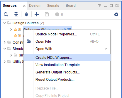
Step 16:
Go to “Sources” tab, right click on “Webserver” design file and select “Create HDL Wrapper”. Click OK on the window that appears to finish generating wrapper.
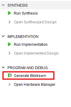
Step 17:
Click “Generate Bitstream” under PROGRAM AND DEBUG section and click “Yes” in any subsequent dialog window which comes up.
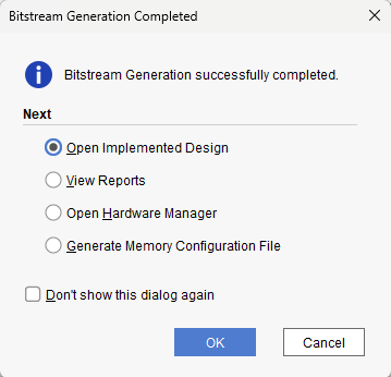
Step 18:
Once the bitstream is successfully generated, close any “Bitstream Generation Completed” dialog which comes up asking for what to do next.
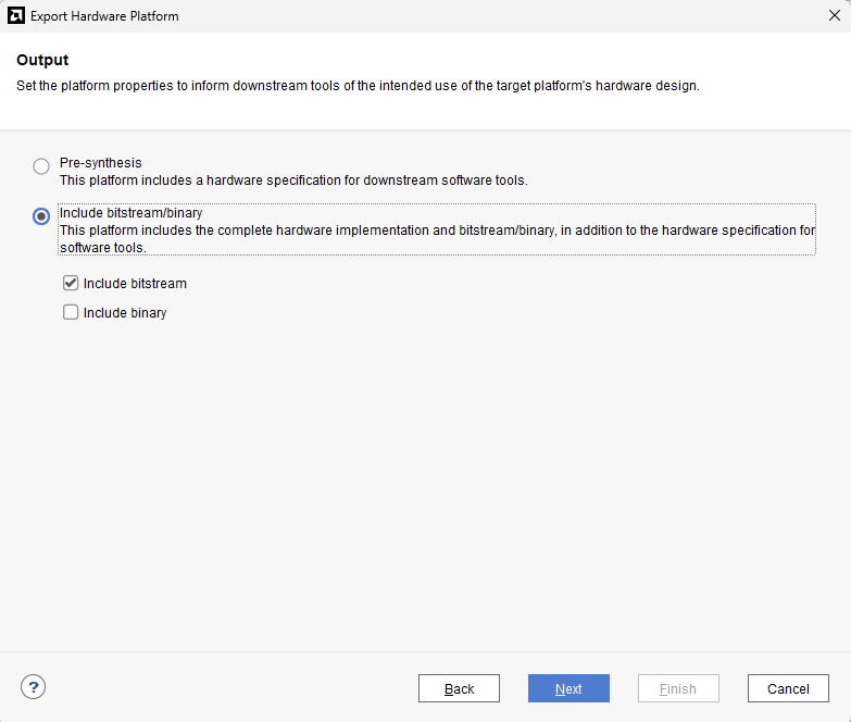
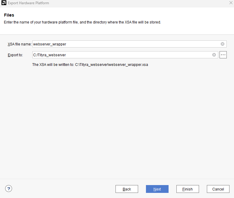
Go to File -> Export -> Export Hardware…
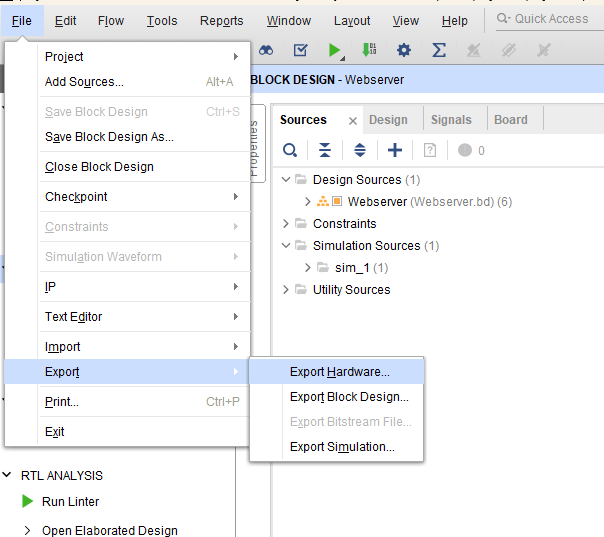
Check “Include bitstream”, keep “Export to:” default, and click OK.
Step 19:
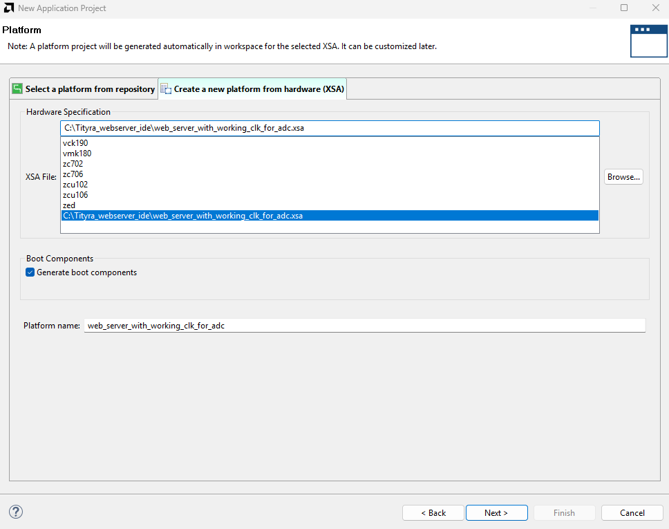
Launch Vitis IDE. In Vitis IDE window, select Create Application Project and click Next in the dialog box that appears.

In the Platform window, select Create a new platform from hardware tab and import the XSA file which is already created (Provide XSA file location). Click Next.
Step 20:
In the Application Project Details window, give an appropriate name for the Vitis Project and click Next. Click Next in the Domain window.
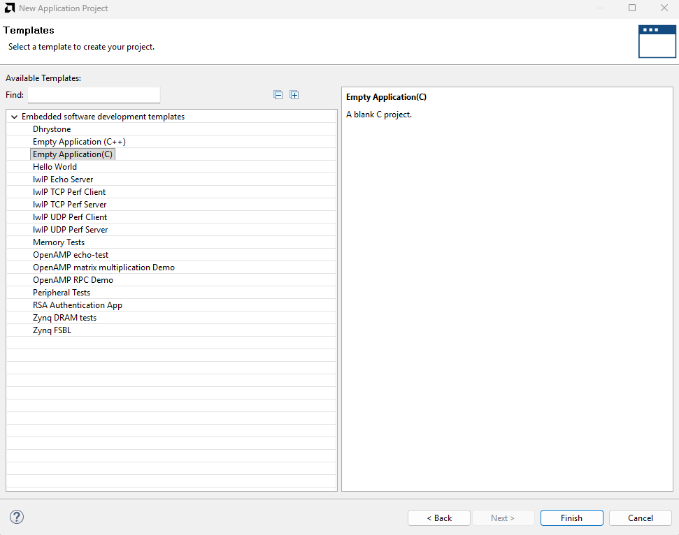
Select the Empty Application(C) template from the list of available templates and click Finish.
Step 21:
Next, in the Explorer panel, locate the newly created empty application.
Right-click on the src folder and select “Import Sources” to add your project files
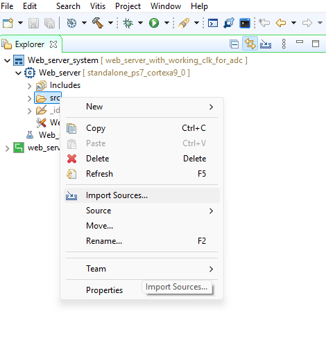
Download the source files from here and save them in a convenient location.
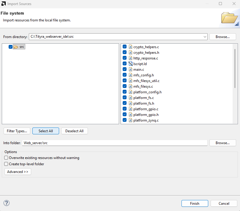
In the window that appears after selecting “Import Sources”, browse to the folder where you saved the files and select the src directory.
Click “Select All”, verify that all source files appear in the right-side panel, and then click Finish to complete the import.
Step 22:
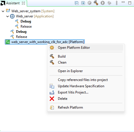
Next, add the lwIP library to the platform you created.
In the Assistant window, right-click on the platform and select “Open Platform Editor” to modify its settings.
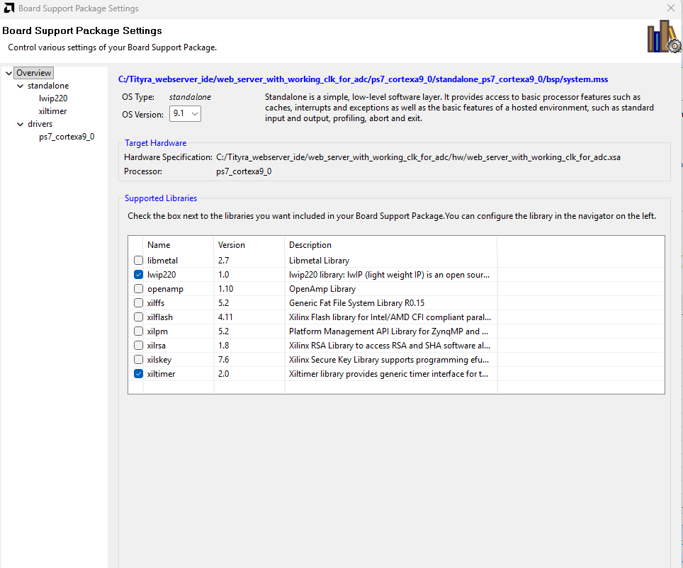
In the platform editor window select the Board support package editor then open the Modify BSP Settings.
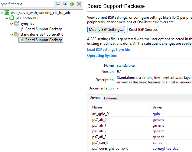
Select the lwip220 and xiltimer library and click ok to apply the changes, then the lwip and xiltimer library will be added to the platform project.
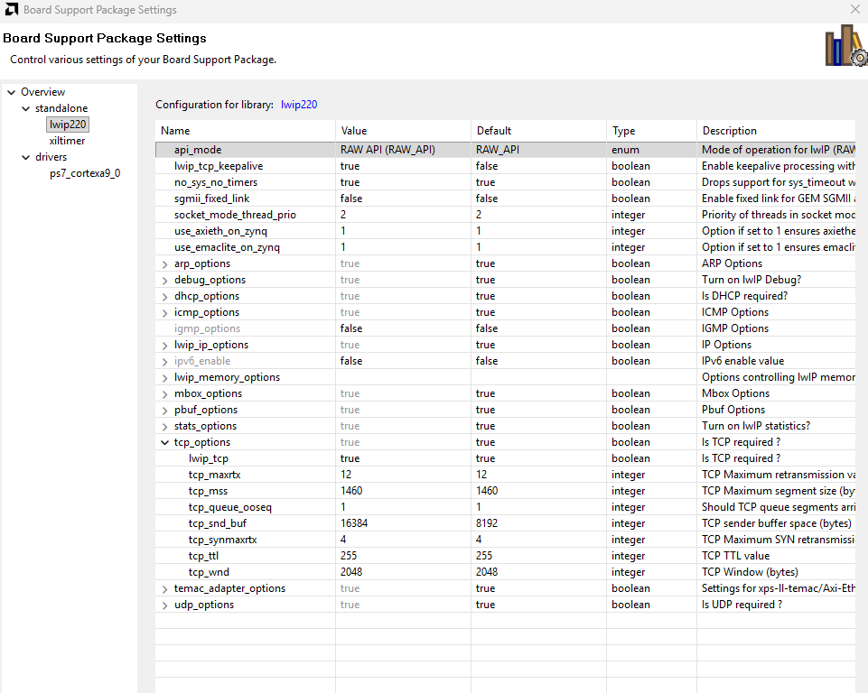
Then open the lwip220 library configuration window and apply the required settings as shown in the reference image.
Make sure to increase tcp_snd_buf to 16384 before saving the configuration.
Step 23:
Press ctrl + B to build everything, once the build is completed successfully, power up TityraCore Zynq 7000 FPGA Development Board using external power supply and connect USB C cable for Serial debugging to the board.
Step 24:
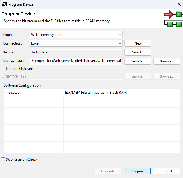
Program the FPGA on Tityra with the generated bitstream and simple bootloop firmware by selecting the “Program Device” option from the “Vitis” menu.
Step 25:
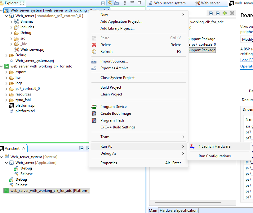
Right-click on the .elf file in the Project Explorer and select “Launch on Hardware” as shown below.
If everything went well, the application running on the board should print as below over the USB UART and should be displayed on the Serial Terminal application.
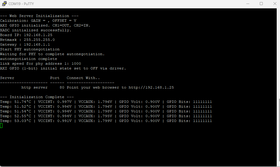
Step 26:
After getting this messages successfully printed on the serial terminal point your web browser to *http://192.168.1.25*** .** Before proceeding, let’s ensure to Change the IPv4 address of the host system to 192.168.1.15 (any IP address can be used) and the default gateway to 192.168.1.1.
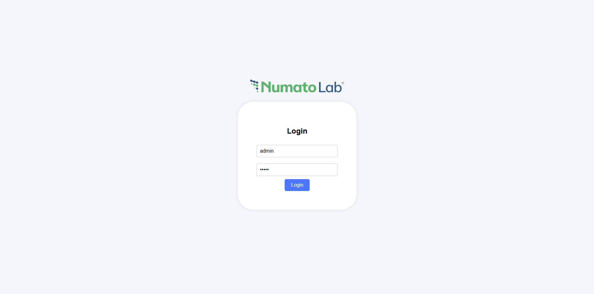
Then you will be able to see the login page of Numato’s Webserver and enter the Username as : admin and Password as: admin
After succesfull login you will be able to see the Demo page where you can see,
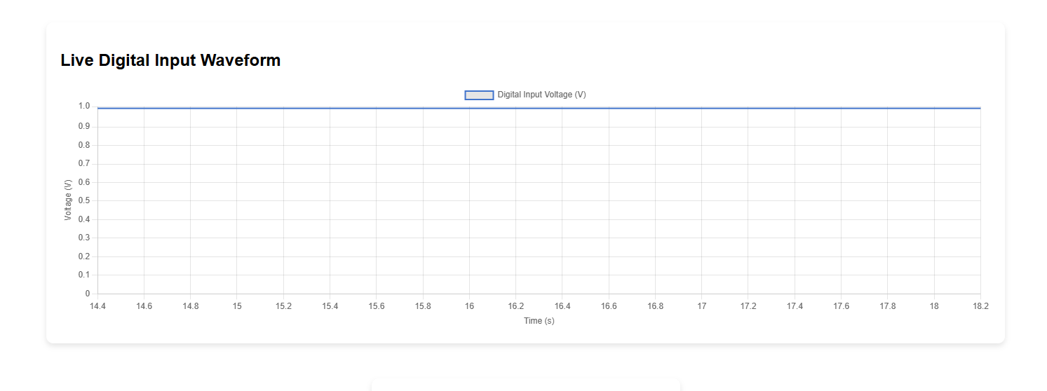
The Live Digital Input Waveform section is the primary demonstration of the Zynq’s high-speed data acquisition capability. It showcases a direct, visual link between an external analog signal and the web interface.
The waveform displayed on the web interface originates from an external signal source: a Function Generator.
- The Function Generator produces a continuous analog voltage signal (e.g., sine wave, square wave, triangle wave).
- This analog signal is provided as the input to the ADC Module (Analog-to-Digital Converter) connected to the Zynq board.
The system is configured to accurately read and represent the input signal within a specific physical limit.
- Input Range: The voltage signal from the function generator must operate within the board’s safe limits, specifically from 0 to 1v.
- A/D Conversion: The ADC module converts the continuously changing analog voltage into discrete digital values (likely 8-bit, 0-255).
- Digital Acquisition: The Zynq’s Programmable Logic (PL) reads these digital values and passes them to the Processing System (PS) for networking.
- Direct Reflection: The voltage measured at the ADC’s input (from 0vto 1v) is immediately reflected as the amplitude of the live waveform graph on the website.
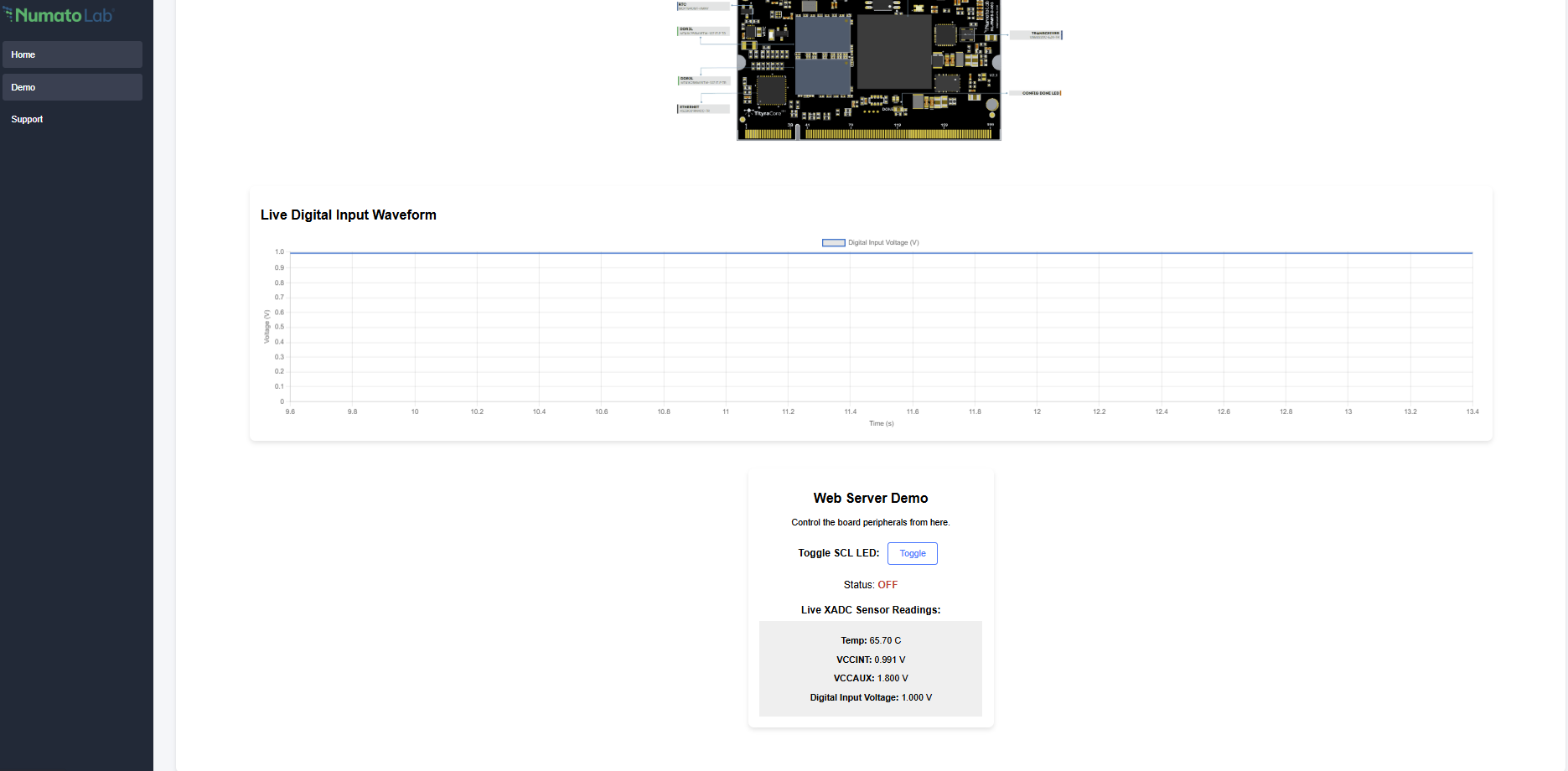
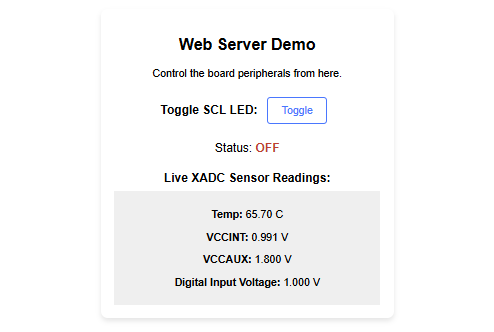
Live XADC Sensor Readings (Monitoring)
- Function: The XADC (Xilinx Analog-to-Digital Converter) is a built-in sensor that monitors the health of the Zynq chip itself.
- What it Reads: It samples and reports the FPGA die temperature and key internal power supply voltages (like VCCINT, VCCAUX).
- Web Action: The website automatically asks the Zynq for this data once every second via the /xadc endpoint.
- Purpose: Allows you to confirm the board is operating within safe temperature and voltage limits.
Toggle SCL LED (Control)
- Function: This demonstrates remote hardware control over the Zynq’s I/O pins from the web.
- How it Works: When you click the “Toggle” button:
- The browser sends an HTTP command (POST request) to the Zynq.
- The Zynq’s software instantly flips the state of a dedicated GPIO pin connected to an external LED.
- Result: The external LED will switch between ON and OFF, and the web status updates to match the physical LED state