Introduction
The purpose of this article is to help readers understand how to use DDR3 memory available on Neso using the AMD MIG 7 IP core easily. The AMD MIG 7 IP core provides users with two interface options: User Interface (a wrapper over Native interface) and the AXI4 Interface. This article will demonstrate how to write to the DDR3 memory on Neso using simple Verilog code and then read back the data. The design will compare the data written to DDR3 and the data read back from it. The verification and DDR3 calibration results will be indicated using the GPIO pins on Neso GPIO header P4.
Prerequisites
To follow this article, you would need the following:
- Hardware:
- Neso Artix 7 FPGA Board
- AMD Platform Cable USB II JTAG debugger (optional)
- Software:
- AMD Vivado Suite 2025.1 or newer
Let’s get started
The following steps will walk you through the process of creating a simple DDR3 project using AMD Vivado.
Step 1:
Start Vivado Design Suite, and select “Create Project” from the Quick Start section. The project wizard will pop up. Press Next to proceed with creating the project.

Step 2:
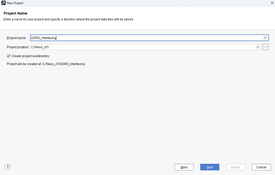
Enter a name for the project and save it at a suitable location. Check the option “Create project subdirectory”. Click Next to continue.
Step 3:
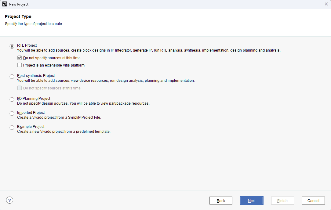
In the Project Type window, select RTL Project and check the option “Do not specify sources at this time”. Click Next.
Step 4:
At the “Default Part” stage, switch to the “Boards” tab and set the vendor to numato.com. Select “Neso” and click Next. If the Neso board does not appear in the list, click “Refresh” to update the board catalog. Vivado will then download the latest board files, after which Neso will become available for selection.
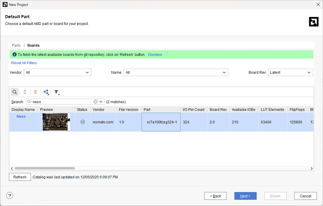
Click Finish to complete creating a new project. A new project will be created by Vivado with the selected settings.
Step 5:
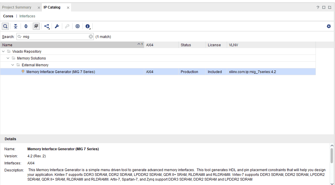
Under the “Flow Navigator”, double-click on “IP Catalogue” to add the necessary IP cores. Search for MIG 7 and double-click on “Memory Interface Generator (MIG 7 Series)” to customize.
Step 6:
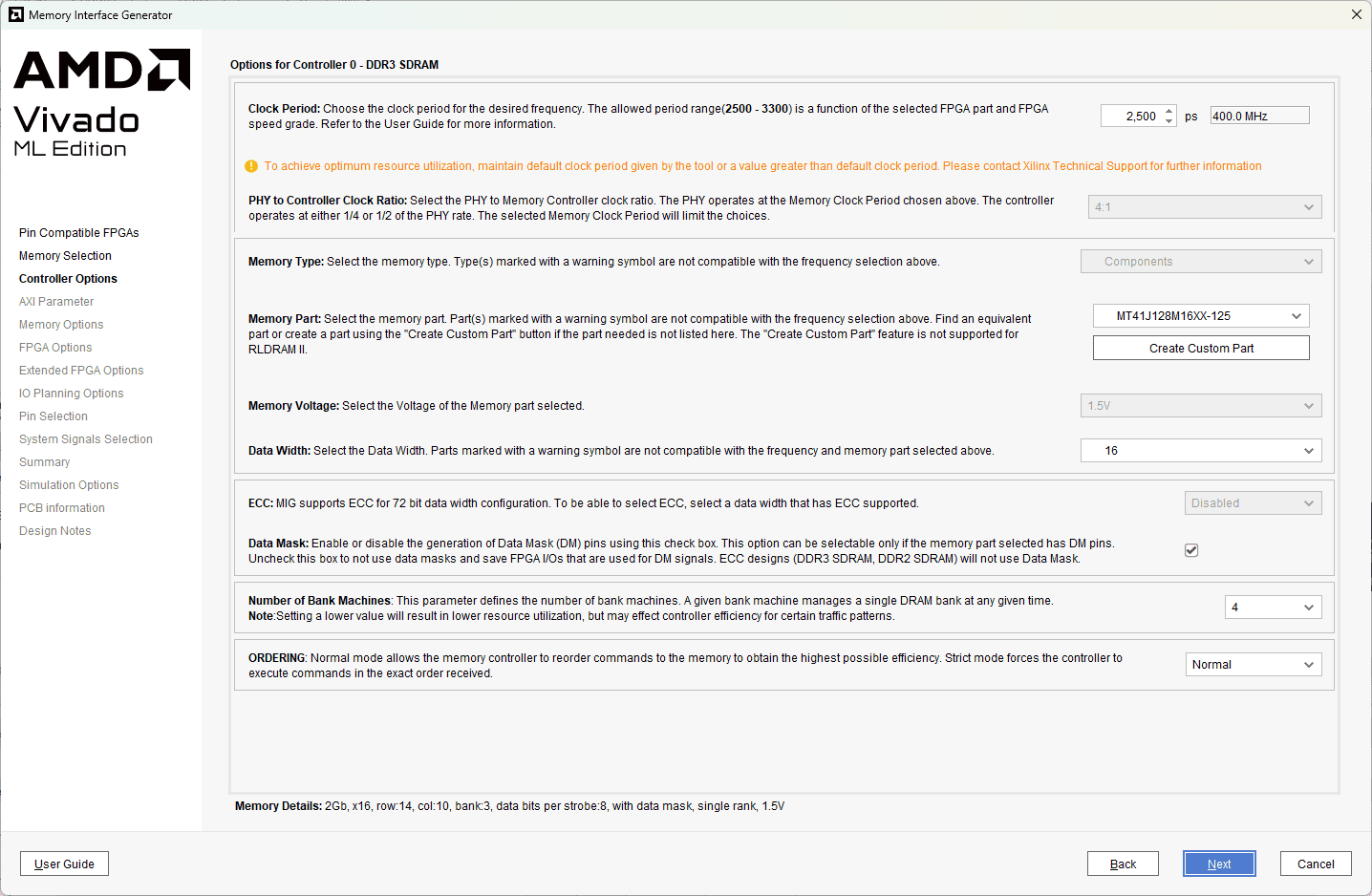
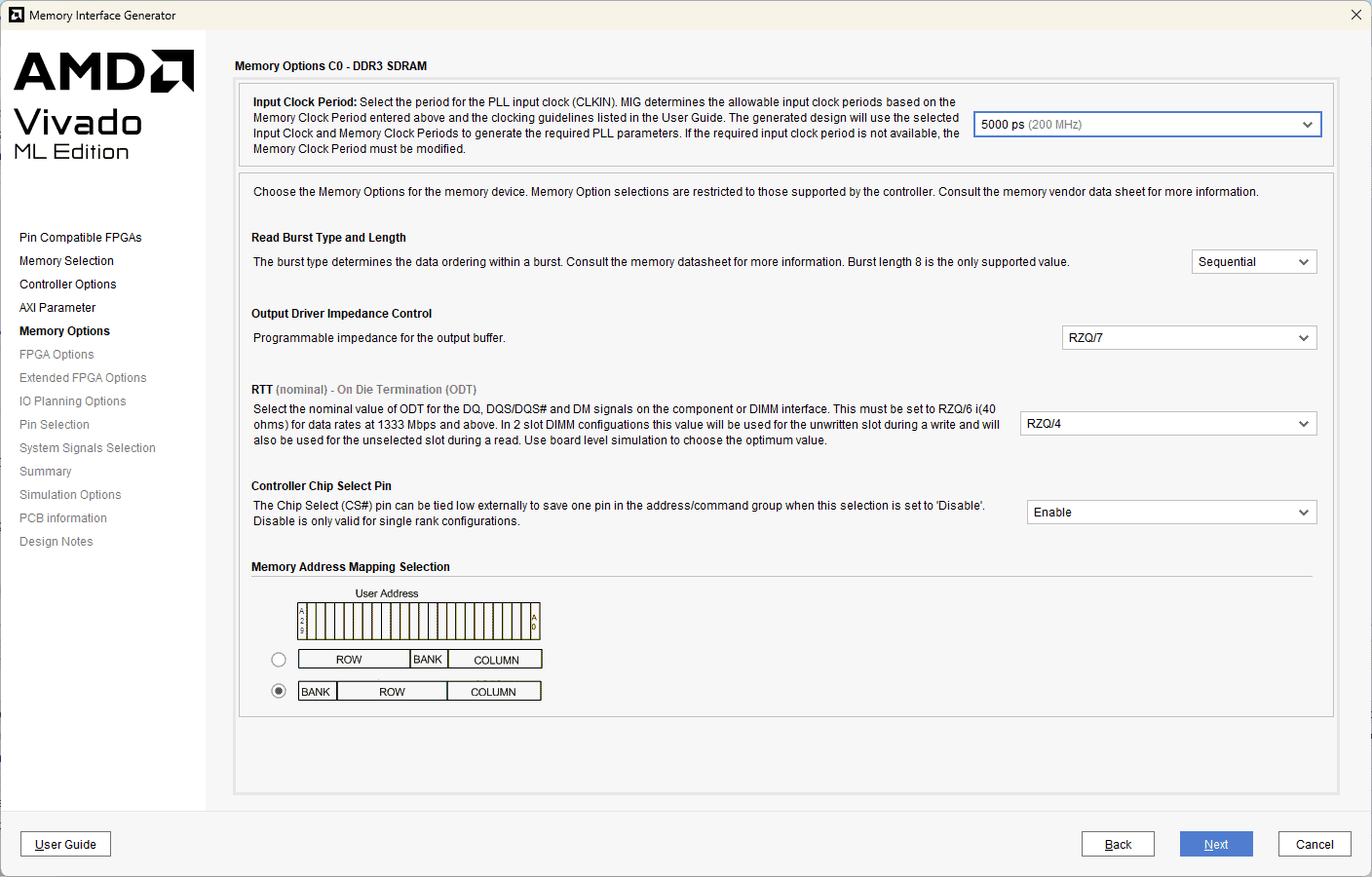
The “AMD Memory Interface Generator” configuration window will open. Click “Next”, select the component name and deselect “AXI4 Interface”. For this example, “mem” is used as a component name. After clicking on “Next” twice, select “DDR3 SDRAM” as Memory. Click “Next”. Select controller options as shown below and click Next. Select “Input Clock Period” as “5000 ps (200MHz) “, keep the remaining settings as default. Click “Next” to proceed.
Step 7:
Select the ‘FPGA options’ as shown below.
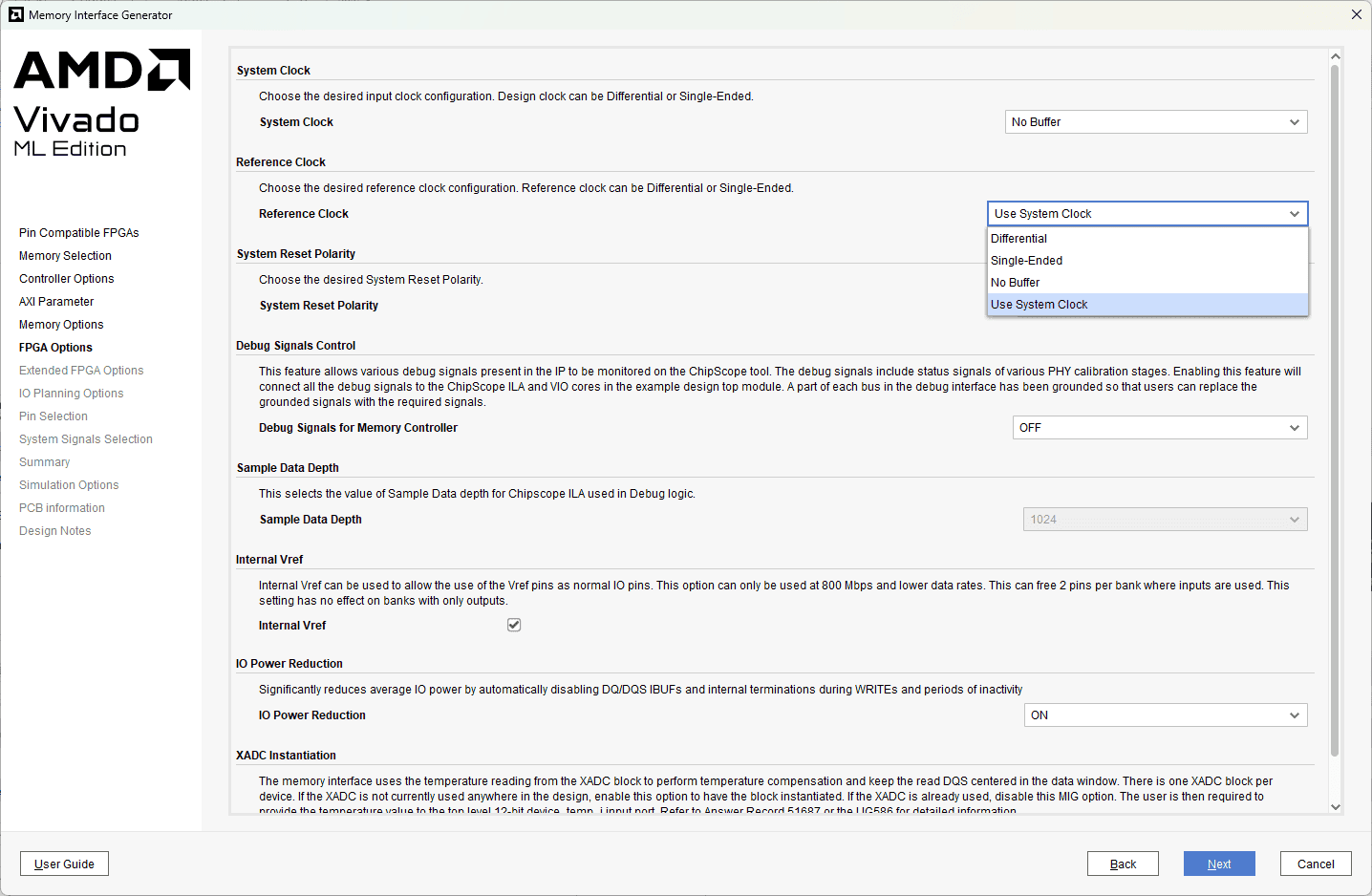
Click Next, choose “Internal Termination Impedance” as “OFF”. Select “Fixed Pin Out” in the next tab and click on “Next”. Assign DDR pins as mentioned in Neso constraints file and validate it by clicking on “Validate”. If the pinout is valid, click “OK” and “Next” to proceed. Accept the license and click “Next” to proceed. Click on “Generate” to generate an IP core with our customised settings.
Step 8:
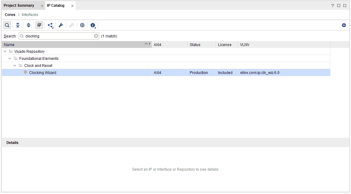
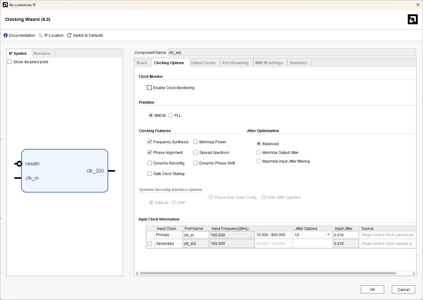
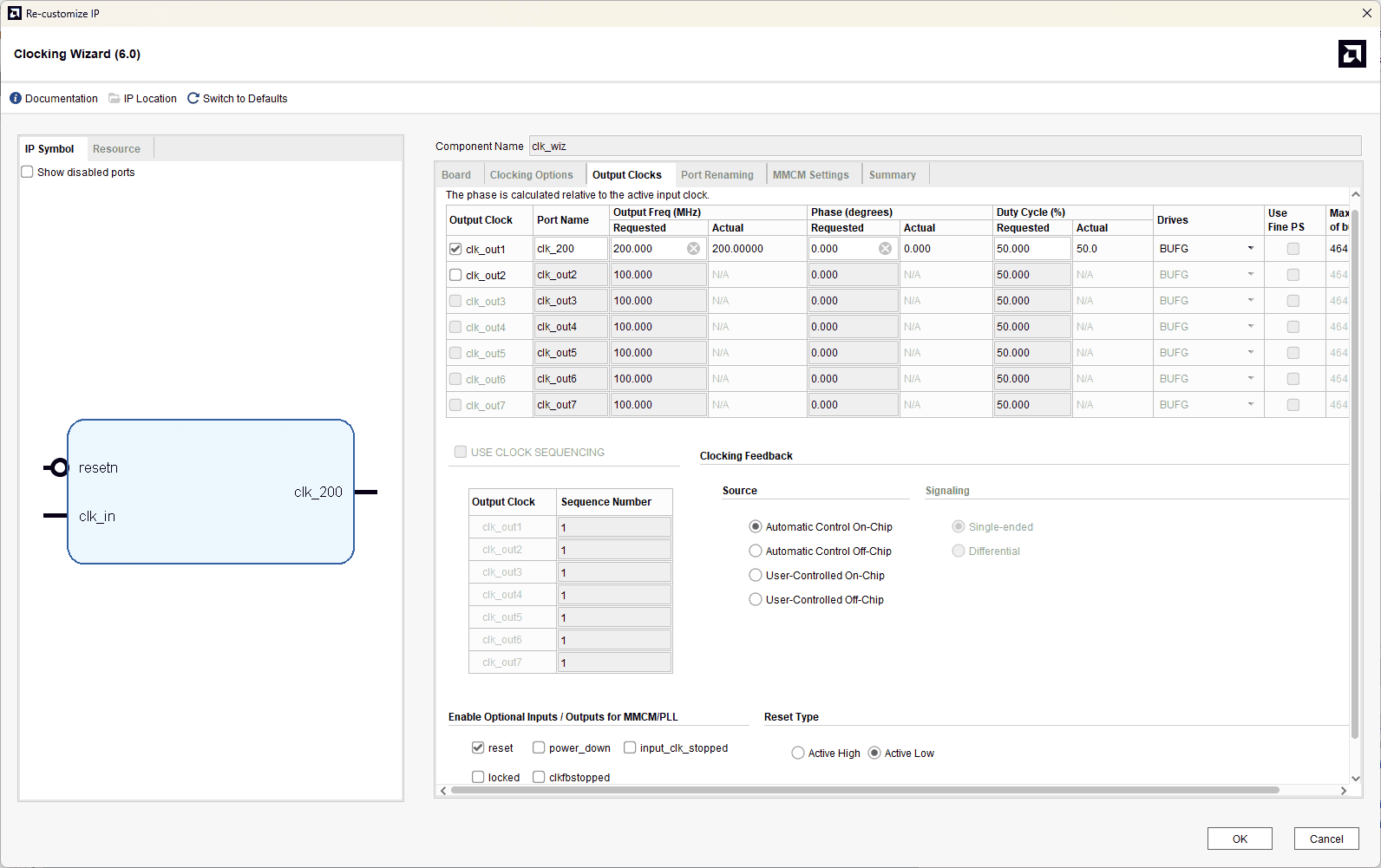
Search for “Clocking Wizard” IP and double-click on it to customise. Choose component name as “clk_wiz”, select “CLK_IN1” board interface to ‘sys_clock’ and “EXT_RESET_IN” to ‘reset’ in the “Board” tab. In “Clocking Options”, choose primary clock port name as “clk_in”, clk_out1 port name as “clk_200”, requested frequency as “200.000”, deselect locked signal, and select “Reset Type” as “Active Low”. Click “OK”.
Step 9 :
Create a Verilog file with the .v extension and copy and paste the following code in “neso_ddr3.v” to run a simple DDR3 with a user interface.
The code uses the AMD MIG7 IP core and the clock wizard IP core in addition to its own logic for interfacing with the MIG 7 IP core. The clock wizard IP is used to generate a 200MHz clock, needed by the MIG 7 IP core, from the 100MHz system clock.
The code basically just implements a simple FSM with six states. Initially, the state machine is in the IDLE state, waiting for the memory calibration to complete. As soon as the calibration is done, the state machine goes into the WRITE state. In this state, the machine waits for the MIG7 IP core to become ready to accept commands and data. When both app_rdy and app_wdf_rdy are asserted by the MIG IP core, which means the core is ready to accept commands and data to write to DDR3. So, the state machine writes data and commands to the MIG IP core and goes into the WRITE_DONE state. In the WRITE_DONE state, the state machine de-asserts the data enable (app_wdf_wren) and command enable (app_en) signals and proceeds to the READ state to read back the data it just wrote to the memory. When in the READ state, the state machine commands the MIG IP core to read the data from memory as soon as the MIG IP core is ready to accept a new command, and then it moves itself to READ_DONE state. When in the READ_DONE state, if app_rd_data_valid the signal is asserted, the state machine captures the data and moves to the PARK state, where it compares the data written to memory with the data read back from memory. If the data matches, led_pass it goes HIGH; otherwise led_fail goes HIGH.
module neso_ddr3(
 input clk_in,

// DDR3 Physical Interface Signals
 //Inouts
 inout  [15:0] ddr3_dq,
 inout  [1:0]  ddr3_dqs_n,
 inout  [1:0]  ddr3_dqs_p,
 // Outputs
 output [13:0] ddr3_addr,
 output [2:0]  ddr3_ba,
 output ddr3_ras_n,
 output ddr3_cas_n,
 output ddr3_we_n,
 output ddr3_reset_n,
 output [0:0] ddr3_ck_p,
 output [0:0] ddr3_ck_n,
 output [0:0] ddr3_cke,
 output [0:0] ddr3_cs_n,
 output [1:0] ddr3_dm,
 output [0:0] ddr3_odt,

// LEDs to signal pass/fail
 output reg  led_pass,
 output reg  led_fail,
 output wire led_calib
 );

 wire calib_done;

 reg  [27:0] app_addr = 0;
 reg  [2:0]  app_cmd = 0;
 reg  app_en;
 wire app_rdy;

 reg  [127:0] app_wdf_data;
 wire app_wdf_end = 1;
 reg  app_wdf_wren;
 wire app_wdf_rdy;

 wire [127:0]app_rd_data;
 wire [15:0] app_wdf_mask = 0;
 wire app_rd_data_end;
 wire app_rd_data_valid;

 wire app_sr_req = 0;
 wire app_ref_req = 0;
 wire app_zq_req = 0;
 wire app_sr_active;
 wire app_ref_ack;
 wire app_zq_ack;

 wire ui_clk;
 wire ui_clk_sync_rst;

 wire sys_clk_i;

 reg [127:0] data_to_write = {32'hcafebabe, 32'h12345678,
                              32'hAA55AA55, 32'h55AA55AA};
 reg [127:0] data_read_from_memory = 128'd0;

 // Power-on-reset generator circuit.
 // Asserts resetn for 1023 cycles, then deasserts
 // `resetn` is Active low reset
 reg [9:0] por_counter = 1023;
 always @ (posedge clk_in) begin
   if (por_counter) begin
     por_counter <= por_counter - 1 ;
   end
end

 wire resetn = (por_counter == 0);

 // Clock Wizard
 // DDR3 core requires 200MHz input clock
 // We generate this clock using AMD Clocking Wizard IP Core
 clk_wiz clk_wiz (
   .clk_in (clk_in),
   .clk_200 (sys_clk_i),
   .resetn (resetn)
 );

// Instatiation of MIG core named `mem`
 mem mem (
   // DDR3 Physical interface ports
   .ddr3_addr   (ddr3_addr),
   .ddr3_ba     (ddr3_ba),
   .ddr3_cas_n  (ddr3_cas_n),
   .ddr3_ck_n   (ddr3_ck_n),
   .ddr3_ck_p   (ddr3_ck_p),
   .ddr3_cke    (ddr3_cke),
   .ddr3_ras_n  (ddr3_ras_n),
   .ddr3_reset_n(ddr3_reset_n),
   .ddr3_we_n   (ddr3_we_n),
   .ddr3_dq     (ddr3_dq),
   .ddr3_dqs_n  (ddr3_dqs_n),
   .ddr3_dqs_p  (ddr3_dqs_p),
   .ddr3_cs_n   (ddr3_cs_n),
   .ddr3_dm     (ddr3_dm),
   .ddr3_odt    (ddr3_odt),

   .init_calib_complete (calib_done),

   // User interface ports
   .app_addr    (app_addr),
   .app_cmd     (app_cmd),
   .app_en      (app_en),
   .app_wdf_data(app_wdf_data),
   .app_wdf_end (app_wdf_end),
   .app_wdf_wren(app_wdf_wren),
   .app_rd_data (app_rd_data),
   .app_rd_data_end (app_rd_data_end),
   .app_rd_data_valid (app_rd_data_valid),
   .app_rdy     (app_rdy),
   .app_wdf_rdy (app_wdf_rdy),
   .app_sr_req  (app_sr_req),
   .app_ref_req (app_ref_req),
   .app_zq_req  (app_zq_req),
   .app_sr_active(app_sr_active),
   .app_ref_ack (app_ref_ack),
   .app_zq_ack  (app_zq_ack),
   .ui_clk      (ui_clk),
   .ui_clk_sync_rst (ui_clk_sync_rst),
   .app_wdf_mask(app_wdf_mask),
   // Clock and Reset input ports
   .sys_clk_i (sys_clk_i),
   .sys_rst (resetn)
   );

 localparam IDLE = 3'd0;
 localparam WRITE = 3'd1;
 localparam WRITE_DONE = 3'd2;
 localparam READ = 3'd3;
 localparam READ_DONE = 3'd4;
 localparam PARK = 3'd5;
 reg [2:0] state = IDLE;

 localparam CMD_WRITE = 3'b000;
 localparam CMD_READ = 3'b001;

 assign led_calib = calib_done;

always @ (posedge ui_clk) begin
  if (ui_clk_sync_rst) begin
    state <= IDLE;
    app_en <= 0;
    app_wdf_wren <= 0;
  end else begin
    case (state)
      IDLE: begin
        if (calib_done) begin
          state <= WRITE;
        end
      end

      WRITE: begin
        if (app_rdy & app_wdf_rdy) begin
          state <= WRITE_DONE;
          app_en <= 1;
          app_wdf_wren <= 1;
          app_addr <= 0;
          app_cmd <= CMD_WRITE;
          app_wdf_data <= data_to_write;
        end
      end

      WRITE_DONE: begin
        if (app_rdy & app_en) begin
          app_en <= 0;
        end

        if (app_wdf_rdy & app_wdf_wren) begin
          app_wdf_wren <= 0;
        end

        if (~app_en & ~app_wdf_wren) begin
          state <= READ;
        end
      end

      READ: begin
        if (app_rdy) begin
          app_en <= 1;
          app_addr <= 0;
          app_cmd <= CMD_READ;
          state <= READ_DONE;
        end
      end

      READ_DONE: begin
        if (app_rdy & app_en) begin
          app_en <= 0;
        end

        if (app_rd_data_valid) begin
          data_read_from_memory <= app_rd_data;
          state <= PARK;
        end
      end

      PARK: begin
        if (data_to_write == data_read_from_memory) begin
          led_pass <= 1;
        end else if (data_to_write != data_read_from_memory) begin
          led_fail <= 1;
        end
      end

      default: state <= IDLE;
   endcase
 end
end

endmodule // top
Step 10:
Create a constraints file and copy-paste the following constraints.
set_property -dict {PACKAGE_PIN A14 IOSTANDARD LVCMOS33} [get_ports led_calib]
set_property -dict {PACKAGE_PIN A13 IOSTANDARD LVCMOS33} [get_ports led_pass]
set_property -dict {PACKAGE_PIN D13 IOSTANDARD LVCMOS33} [get_ports led_fail]
Step 11:
Generate Bitstream by clicking on “Generate Bitstream”. Once the Bitstream is generated successfully, power up Neso and program the device.
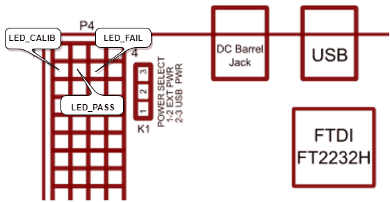
FPGA pins A14, A13 and D13 which are in the 2nd row of GPIO Header P4 are connected to led_calib, led_pass and led_fail signals respectively. After programming, make sure that led_calib (calibration done) signal goes HIGH, indicating that initial calibration was completed successfully. Also, led_pass it should go HIGH, indicating that data was written to memory and read back successfully. led_fail should stay LOW since led_fail Being HIGH indicates a failed attempt to write and read data from memory. The picture below illustrates the FPGA pins on the Neso Artix 7 FPGA Module GPIO header used for status indication.
You can use either an LED with a series resistor or a multimeter to measure the output of led_calib, led_pass and led_fail signals. If you observe led_calib and led_pass LEDs high and led_fail LED stays low, then your Neso Artix 7 DDR3 example design worked. Congratulations!