Introduction
USB 3.0 has revolutionized the world of desktops and mobile devices by bringing much higher bandwidth and better power delivery compared to its predecessor USB 2.0. USB 3.0 (later renamed as USB 3.1 Gen 1) offers data rate of 5Gb/s or a whopping theoretical bandwidth of 625MB/s[1]. This is more than 10 times the theoretical maximum bandwidth of USB 2.0.[2] While practically available bandwidth for end user applications can be lower depending on the hardware and firmware solutions chosen(will discuss this later in this document), USB 3.0 offers a great value proposition that cannot be ignored. Other host interface solutions available in the market such as PCI Express, Thunderbolt and Ethernet can outperform USB 3.0 in many scenarios, but all these interfaces are relatively more expensive to implement especially in low volume segments. Also, USB 3.0 offers better power delivery compared to the other available solutions. This can further reduce the total cost of the solution/end product.
![Figure 1 - A Rendering of Callisto K7 USB3.0 Kintex 7 FPGA Module from Numato Lab [Courtesy Numato Systems Pvt. Ltd.]](https://numato.com/wp-content/uploads/2018/06/CallistoK7-3D.png)
Figure 1 – A Rendering of Callisto K7 USB3.0 Kintex 7 FPGA Module from Numato Lab [Courtesy Numato Systems Pvt. Ltd.]
This whitepaper assumes a Xilinx FPGA is used in the solution. But the principles can be applied to most commercially available FPGA with certain exclusions.
A USB Primer
Universal Serial Bus also known popularly as USB is a standard developed by USB Implementers Forum (USB-IF). Released in 1996, the standard specifies Cables, Connectors, Protocols and Power Delivery between Personal Computers/Mobile Devices and Peripheral Devices. USB was designed from the ground up to eventually replace legacy peripheral connectivity solutions such as Serial Ports and Printer Ports. This is achieved by defining several Device Classes such as Human Interface Device Class (HID), Printer class etc. USB defines four types of transfers – Control, Isochronous, Bulk and Interrupt. Each transfer type offers varying bandwidth and different delivery guarantees, usually trading one with the other. Transfers happen between logical data source/sink pairs established in host and peripheral known as Endpoints. The concept of Endpoint offers easy segregation of traffic and allows multiple agents on the Host and Device communicate transparently despite the fact that USB has only one pair of RX/TX physical channels to share. A logical connection between a pair of corresponding Endpoints on Host and Device is known as a Pipe. Host agents such as applications and drivers can open a Pipe to the peripheral device and do reads and write to move data. Endpoints are grouped in to Interfaces that represent part of a device function. For example, USB CDC class devices use control Endpoints for enumeration and device management, Interrupt Endpoints for event notifications and Bulk Endpoints for data transfer. Certain devices support more than one function and are called composite devices.
USB 3.0 is the third revision of USB specification rolled out by USB Implementers Forum which supersedes USB 2.0. USB 3.0 offers lots of improvements in bandwidth, power management and delivery, efficient bus usage etc. USB 3.0 connector defines a pair of USB2.0 compatible signals (D+/D-) to ensure that USB 3.0 hosts are compatible with USB2.0 legacy devices. The SuperSpeed transmitter and receiver differential pairs provides the 5.0Gbps channel for USB3.0 “SuperSpeed” data transfers. As one can see later in the document, availability of a USB 2.0 interface on the same connector is very useful for designs containing FPGA device as it provides a sideband mechanism to provide other services such as FPGA configuration, Board health monitoring services, Power supply configuration etc… without sacrificing bandwidth on the USB3.0 channel. USB 2.0 can also be used as a fallback channel when the upstream host or hub that does not support USB3.0. Examples of utilizing the USB2.0 channel for other purposes is explained elsewhere in this document. USB 3.0 was renamed to USB 3.1 Gen 1 in July 2013. USB 3.1 Gen 2 specification defines a “SuperSpeed+” transfer mode at a rate of 10Gbps. USB 3.2 is in the horizon that offers up to 20Gbps over two lanes on a USB Type C connector.
Why Choose USB 3.0
Of all the potentially available host interface options, why should a system designer choose USB 3.0? Some of the reasons for and against USB3.0 are summarized in the table below.
| Technology | Good | Not so good |
|---|---|---|
| USB 3.0 | – High bandwidth at disposal – USB 2.0 available on same connector and can be used as sideband – Relatively inexpensive – Off-the-shelf solutions available – Better power delivery | – Superspeed differential signals are quite fast and special care must be taken while designing hardware |
| USB 2.0 | – Large variety of off-the-shelf solutions available – Very inexpensive – Power delivery available | – Limited bandwidth |
| PCI Express | – Very high bandwidth – Flexible bandwidth by adding additional lanes | – Very careful hardware design required – Not very mobile |
| Thunderbolt | – Very high bandwidth | – No off-the-shelf solutions available |
| Ethernet | – Large number of off-the-shelf solutions available | – Higher latency – Power delivery only available through specialized equipment (PoE) |
| Wi-Fi | – Wireless | – Higher latency – Limited bandwidth – No power delivery |
As the table summarizes, USB 3.0 stands out in the crowd as one of the best solutions available today for low latency, high bandwidth, low cost FPGA host interface.
Selecting an Optimal USB 3.0 Solution
As of writing this document, there are several USB 3.0 options to choose from. Depending on the needs of the system, cost and other factors one or the other may be better suited for a specific design. A few of the options are listed below.
- Use USB 3.0 Physical Layer transceiver with PIPE interface such as TI TUSB1310
- Use a FPGA with dedicated USB 3.0 peripheral device (Example, Xilinx Zynq Ultrascale+ [3])
- Use a general-purpose USB 3.0 peripheral controller such as Cypress EZ-USB® FX3™
- Use a USB 3.0 FIFO bridge solution such as FTDI FT60X
We continue analyzing option 4 (using an off-the-shelf USB 3.0 FIFO bridge) for the reasons listed below. Readers may find other options better suited for their specific scenarios based on the specific design, cost and time to market needs. Researching those options are left to the reader.
- USB 3.0 FIFO bridges works transparently. Usually no knowledge of underlying USB protocol is required.
- Available off-the-shelf and inexpensive
- Takes up minimal resources on the FPGA. Thus, making most of the FPGA resources available to user design.
- USB 3.0 FIFO bridges are fully stand alone and no firmware development efforts required
A Proposed Solution using FTDI FT601 and FT2232H
A fully functional FPGA Host Interface solution can be designed by using the following devices.
- FTDI FT601 USB 3.0 FIFO Bridge as the main data pipe
- FTDI FT2232H connected to the USB 2.0 interface through a USB hub as sideband bridge
- Microchip USB2422 USB 2.0 hub for making the USB2.0 link available to both FT601 and FT2232H
FTDI FT600 offers an easy to use USB 3.0 FIFO bridge interface that can be integrated to designs with minimal complexity. It has two upstream interfaces, a USB 3.0 interface and a USB2.0 interface. In normal configurations, the USB 2.0 upstream interface is connected to the USB2.0 signals (D+/D-) of the upstream USB C connector as shown in figure 2.
![Figure 2 - Suggested FT60x upstream connection by manufacturer (Courtesy Future Technology Devices International Ltd [4])](https://numato.com/wp-content/uploads/2018/06/FT60x-upstreamconnection.png)
Figure 2 – Suggested FT60x upstream connection by manufacturer (Courtesy Future Technology Devices International Ltd [4])
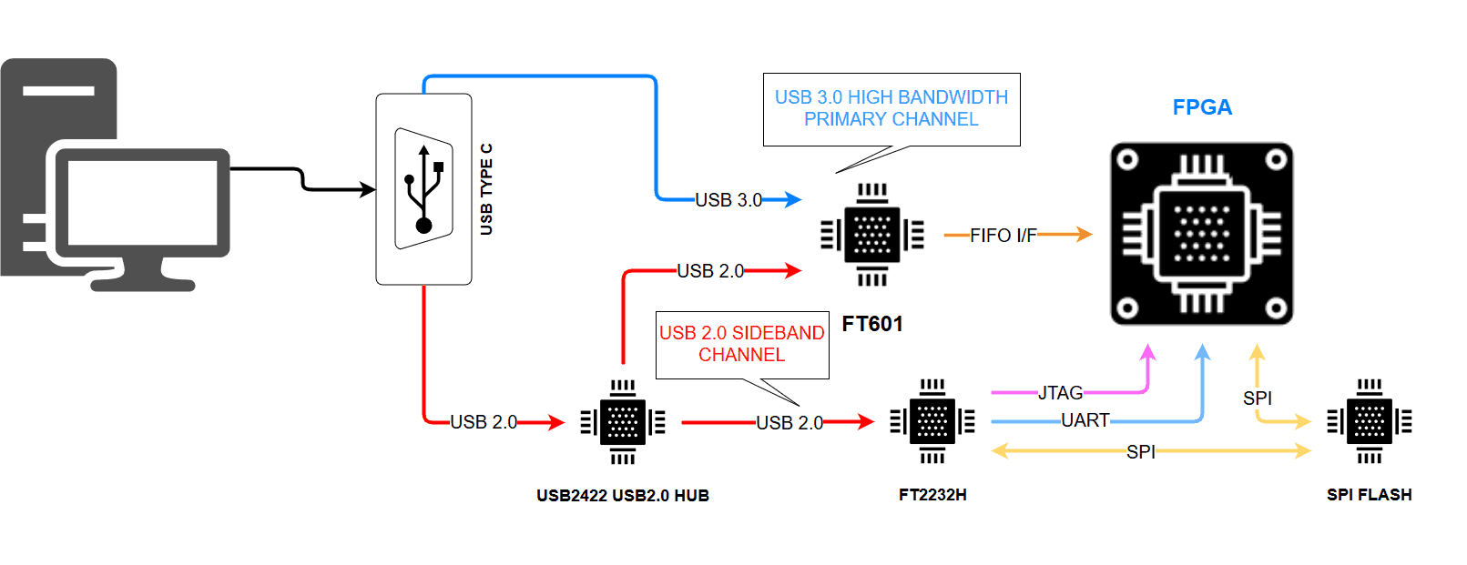
Figure 3 – A proposed USB3.0 Host Interface Solution using FT601
Another possibility is to connect FT2232 Bus A to JTAG interface of FPGA to access the FPGA’s JTAG state machine directly. This way, a host software/script can use this interface to program and test the solution. The FT2232H Bus B could be used for UART interface for debugging or user interface which can be very useful during development phase.
As for the USB 3.0 side of the picture, the FT601 provides a 32-bit FIFO interface to the FPGA which can run at maximum of 100MHz. So, the theoretical maximum bandwidth which can be extracted using FT601 would be 100 MHz * 32 bits / 8 bits-per-byte = 400 MB/s, assuming a 4-byte transfer every clock cycle. The FTDI have practically tested the maximum bandwidth using FT601 up to 363.93 MB/s[5]. This amount of bandwidth enables many applications such as Full HD video streaming to/from FPGA, Data Acquisition, Software Defined Radio etc.
FT601 offers two main options for interfacing with FPGA: the 245 FIFO protocol and the Multi-channel FIFO protocol. The Multi-channel FIFO protocol provides 4 independent bulk IN/OUT endpoints to transfer. FT601 arbitrates fairly between the 4 channels so users can implement their designs without worrying about multiplexing data from multiple channels into a single USB bus themselves. Two general purpose I/Os are also available for any side-band usage, such as LED notifications, configuration signals etc. The D3XX driver and API provided by FTDI makes host software development easier [6].
Conclusion
With wider market adoption, high usable bandwidth and great power delivery, USB 3.0 is a great choice when considering host interface options for your next FPGA solution design. Off the shelf solutions available from vendors such as FTDI and Cypress Semiconductors makes design and manufacturing much easier. Numato Lab has selected USB 3.0 as the host interface for several of their FPGA products due to aforementioned reasons. A list of Numato Lab’s FPGA products can be found at https://numato.com/.
References
- https://en.wikipedia.org/wiki/USB_3.0
- http://sdphca.ucsd.edu/Lab_Equip_Manuals/usb_20.pdf
- https://www.xilinx.com/support/documentation/data_sheets/ds891-zynq-ultrascale-plus-overview.pdf
- http://www.ftdichip.com/Support/Documents/DataSheets/ICs/DS_FT600Q-FT601Q%20IC%20Datasheet.pdf
- http://www.ftdichip.com/Support/Documents/AppNotes/AN_386%20FTDI%20FT600%20Maximize%20Performance.pdf
- http://www.ftdichip.com/Drivers/D3XX.htm
Trademarks
- NUMATO LAB® is a trademark of Numato Systems Pvt. Ltd.
- EZ-USB® and FX3™ are trademarks of Cypress Semiconductor Corporation
- Xilinx, UltraScale+, Zynq and Kintex are trademarks of Xilinx, Inc
All other trademarks are property of their registered owners.