Introduction
The purpose of this article is to help readers understand how to use LPDDR memory available on Waxwing using Xilinx MIG 6 IP core easily. The MIG 6 IP core provides users with two interface options: User Interface (a wrapper over Native memory interface) and the AXI4 Interface. This article will demonstrate how to write to the LPDDR memory on Waxwing using simple Verilog code and then read back the data. The design will compare the data written to LPDDR and the data read back from it. The verification results and LPDDR calibration results are indicated using onboard LEDs on Waxwing.
Prerequisites
To follow this article, you would require following:
- Hardware:
- Waxwing Spartan 6 FPGA Development Board
- Xilinx Platform Cable USB II JTAG debugger (optional).
- Software:
- Xilinx ISE Design Suite 14.7
Let’s get started
The following steps will walk you through the process of creating simple LPDDR project for Waxwing using Xilinx ISE.
Step 1:
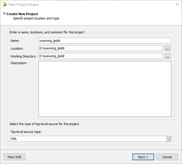
Open Xilinx ISE Design Suite and select “New Project” from “File” menu. “New Project” dialog will open. Type in a project name and select a convenient project location. In this article, author has used “waxwing_lpddr” as a project name. Click “Next” to proceed.
Step 2:
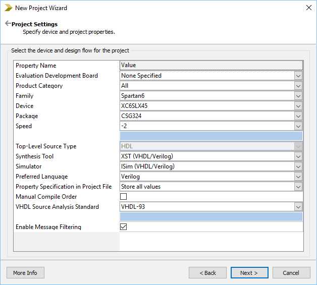
Specify the device and project settings (Family: Spartan 6, Device: XC6SLX45, Package: CSG324 and Speed grade: -2) as shown below in the “Project Settings” tab. Click “Next” and “Finish”. A new ISE project will open with the selected settings.
Step 3:
Under the “Design” tab, right click and select “New Source”. “New Source Wizard” dialog will open. Select “IP (CORE Generator & Architecture Wizard)”, type in “File Name” as “mem” and click “Next” to proceed. Select “MIG 6” IP core, click “Next” and “Finish”. “Xilinx Memory Interface Generator” wizard will open. Click “Next” three consecutive times, select “LPDDR” as “Memory Type” and de-select “Enable AXI interface for All MCBs”. Click “Next” to proceed.
Step 4:
Select the “Frequency” as “10000 ps (100MHz)” and “MT46H32M16XXXX-5” as Memory Part. Click “Next” twice and select port configuration as “One 128-bit bidirectional port”, under “Configuration Selection” tab. Leave the other options as default. Click “Next” twice and choose “System Clock” as “Single-Ended”. Accept the license by clicking on the “Next” twice. Click “Next” and “Generate”. The MIG 6 IP core is generated.
Step 5:
Create a Verilog file with .v extension and copy paste the following code in “waxwing_lpddr.v” to run simple LPDDR project with the user interface.
The RTL code uses MIG 6 IP core and the input clock for the MIG is directly provided from the 100MHz onboard oscillator on Waxwing.
To interface with memory controller IP core, a simple FSM is implemented with six states. The states are IDLE, WR_CMD, WRITE, RD_CMD, READ and PARK. Initially, the FSM is in the IDLE state. The state machine waits for the calibration to complete in the IDLE state. When the calibration completes successfully (led_calib goes HIGH), the state machine changes to WR_CMD state.
In WR_CMD state, the state machine waits for the MIG to be ready to accept commands. When the c3_p0_cmd_full signal gets de-asserted, the core is ready to accept the write command. The state machine writes the command to the MIG IP core and changes its state to WRITE. In WRITE state, the state machine de-asserts command enable (c3_p0_cmd_en) and waits for the MIG to become ready to accept new data to be written to memory. When the c3_p0_wr_full signal is de-asserted by the MIG core, the write enable signal (c3_p0_wr_en) is asserted and the data is captured into the write FIFO of MIG 6 core. The state machine goes to RD_CMD state to read back the data from MIG.
In RD_CMD state, the state machine again waits for the MIG to become ready to accept commands. When the c3_p0_cmd_full signal is de-asserted by the MIG IP core, it indicates that the core is ready to accept the command for reading. The state machine de-asserts the write enable (c3_p0_wr_en) signal, writes the command to the MIG IP core and changes its state to READ. In READ state, the state machine de-asserts the command enable (c3_p0_cmd_en) signal and waits for the read empty signal from the MIG 6 IP core to go low. If the read empty signal is low, it indicates that data, as requested by the design from LPDDR, is now available in the MIG core’s read FIFOto be read from it. So, when c3_p0_rd_empty gets de-asserted by the MIG, the state machine asserts the read enable signal (c3_p0_rd_en) and data is captured from the MIG IP core’s FIFO to data_read_from_memory register. The state machine changes to PARK state where the data written to the memory is compared with the data read back from memory.
In the PARK state, if the data written to the memory and the data read back from it match, thenled_pass goes HIGH otherwise led_fail goes HIGH.
module waxwing_lpddr(
   input         clk_in,
   input         reset,
   inout  [15:0] mcb3_dram_dq,
   output [12:0] mcb3_dram_a,
   output [1:0]  mcb3_dram_ba,
   output        mcb3_dram_ras_n,
   output        mcb3_dram_cas_n,
   output        mcb3_dram_we_n,
   output        mcb3_dram_cke,
   output        mcb3_dram_dm,
   inout         mcb3_dram_udqs,
   inout         mcb3_rzq,
   output        mcb3_dram_udm,
   inout         mcb3_dram_dqs,
   output        mcb3_dram_ck,
   output        mcb3_dram_ck_n,
   output        led_calib,
   output  reg   led_pass,
   output  reg   led_fail
   );

 wire                c3_clk0;
 wire                c3_rst0;
 // Command Signals
 wire                c3_p0_cmd_clk;
 reg                 c3_p0_cmd_en;
 reg    [2:0]        c3_p0_cmd_instr;
 reg    [5:0]        c3_p0_cmd_bl;
 reg    [29:0]       c3_p0_cmd_byte_addr;
 wire                c3_p0_cmd_empty;
 wire                c3_p0_cmd_full;
 // Write Signals
 wire                c3_p0_wr_clk;
 reg                 c3_p0_wr_en;
 wire   [15:0]       c3_p0_wr_mask;
 reg    [127:0]      c3_p0_wr_data;
 wire                c3_p0_wr_full;
 wire                c3_p0_wr_empty;
 wire   [6:0]        c3_p0_wr_count;
 wire                c3_p0_wr_underrun;
 wire                c3_p0_wr_error;
 // Read Signals
 wire                c3_p0_rd_clk;
 reg                 c3_p0_rd_en;
 wire   [127:0]      c3_p0_rd_data;
 wire                c3_p0_rd_full;
 wire                c3_p0_rd_empty;
 wire   [6:0]        c3_p0_rd_count;
 wire                c3_p0_rd_overflow;
 wire                c3_p0_rd_error;

 reg  [2:0]  state;
 reg  [127:0]data_read_from_memory = 128'd0;
 wire [127:0]data_to_write = {32'hcafebabe, 32'h12345678,
                              32'hAA55AA55, 32'h55AA55AA};

assign c3_p0_cmd_clk = c3_clk0;
assign c3_p0_wr_clk  = c3_clk0;
assign c3_p0_rd_clk  = c3_clk0;

// Instantiation of memory
 mem u_mem (
   .c3_sys_clk         (clk_in),
   .c3_sys_rst_i       (reset),

   .mcb3_dram_dq       (mcb3_dram_dq),
   .mcb3_dram_a        (mcb3_dram_a),
   .mcb3_dram_ba       (mcb3_dram_ba),
   .mcb3_dram_ras_n    (mcb3_dram_ras_n),
   .mcb3_dram_cas_n    (mcb3_dram_cas_n),
   .mcb3_dram_we_n     (mcb3_dram_we_n),
   .mcb3_dram_cke      (mcb3_dram_cke),
   .mcb3_dram_ck       (mcb3_dram_ck),
   .mcb3_dram_ck_n     (mcb3_dram_ck_n),
   .mcb3_dram_dqs      (mcb3_dram_dqs),
   .mcb3_dram_udqs     (mcb3_dram_udqs), // for X16 parts
   .mcb3_dram_udm      (mcb3_dram_udm), // for X16 parts
   .mcb3_dram_dm       (mcb3_dram_dm),
   .c3_clk0            (c3_clk0),
   .c3_rst0            (c3_rst0),
   .c3_calib_done      (led_calib),
   .mcb3_rzq           (mcb3_rzq),
   .c3_p0_cmd_clk      (c3_p0_cmd_clk),
   .c3_p0_cmd_en       (c3_p0_cmd_en),
   .c3_p0_cmd_instr    (c3_p0_cmd_instr),
   .c3_p0_cmd_bl       (c3_p0_cmd_bl),
   .c3_p0_cmd_byte_addr(c3_p0_cmd_byte_addr),
   .c3_p0_cmd_empty    (c3_p0_cmd_empty),
   .c3_p0_cmd_full     (c3_p0_cmd_full),
   .c3_p0_wr_clk       (c3_p0_wr_clk),
   .c3_p0_wr_en        (c3_p0_wr_en),
   .c3_p0_wr_mask      (c3_p0_wr_mask),
   .c3_p0_wr_data      (c3_p0_wr_data),
   .c3_p0_wr_full      (c3_p0_wr_full),
   .c3_p0_wr_empty     (c3_p0_wr_empty),
   .c3_p0_wr_count     (c3_p0_wr_count),
   .c3_p0_wr_underrun  (c3_p0_wr_underrun),
   .c3_p0_wr_error     (c3_p0_wr_error),
   .c3_p0_rd_clk       (c3_p0_rd_clk),
   .c3_p0_rd_en        (c3_p0_rd_en),
   .c3_p0_rd_data      (c3_p0_rd_data),
   .c3_p0_rd_full      (c3_p0_rd_full),
   .c3_p0_rd_empty     (c3_p0_rd_empty),
   .c3_p0_rd_count     (c3_p0_rd_count),
   .c3_p0_rd_overflow  (c3_p0_rd_overflow),
   .c3_p0_rd_error     (c3_p0_rd_error)
   );

localparam IDLE    = 3'h0,
           WR_CMD  = 3'h1,
           WRITE   = 3'h2,
           RD_CMD  = 3'h3,
           READ    = 3'h4,
           PARK    = 3'h5;
assign c3_p0_wr_mask = 16'h0000;
//****************** State Machine start here ****************************//
always@(posedge c3_clk0)
begin
   if(c3_rst0) begin
      c3_p0_cmd_byte_addr <= 0;
      c3_p0_cmd_bl    <= 1;
      state           <= IDLE;
      c3_p0_cmd_instr <= 3'b000;
      c3_p0_cmd_en    <= 1'b0;
      c3_p0_wr_en     <= 1'b0;
      c3_p0_rd_en     <= 1'b0;
      led_pass        <= 1'b0;
      led_fail        <= 1'b0;
   end
   else begin
      case(state)
         IDLE : begin
           if(led_calib) begin
              state <= WR_CMD;
           end
         end

         WR_CMD : begin
            if(~c3_p0_cmd_full) begin
               c3_p0_cmd_byte_addr <= 0;
               c3_p0_cmd_bl    <= 1;
               c3_p0_cmd_instr <= 3'b000;
               c3_p0_cmd_en    <= 1'b1;
               state           <= WRITE;
            end
         end

         WRITE : begin
            c3_p0_cmd_en     <= 1'b0;
            if(~c3_p0_wr_full) begin
               c3_p0_wr_en   <= 1'b1;
               c3_p0_wr_data <= data_to_write;
               state         <= RD_CMD;
            end
         end


         RD_CMD : begin
            if(~c3_p0_cmd_full) begin
               c3_p0_wr_en         <= 1'b0;
               c3_p0_cmd_byte_addr <= 0;
               c3_p0_cmd_bl        <= 1;
               c3_p0_cmd_instr     <= 3'b001;
               c3_p0_cmd_en        <= 1'b1;
               state               <= READ;
            end
         end

         READ : begin
            c3_p0_cmd_en   <= 1'b0;
            if(~c3_p0_rd_empty) begin
               c3_p0_rd_en <= 1'b1;
               data_read_from_memory <= c3_p0_rd_data;
               state       <= PARK;
            end
         end

         PARK : begin
            c3_p0_rd_en <= 1'b0;
            if (data_to_write == data_read_from_memory) begin
               led_pass <= 1;
           end else if (data_to_write != data_read_from_memory) begin
               led_fail <= 1;
           end
        end

        default: state <= IDLE;
      endcase
   end
end

endmodule
Step 6:
Create a constraints file and copy-paste the following constraints.
CONFIG VCCAUX = "3.3" ;

NET "clk_in" LOC = V10 | IOSTANDARD = LVCMOS33 | PERIOD = 100MHz;
NET "reset" LOC = A11 | IOSTANDARD = LVCMOS33 | DRIVE = 8 | SLEW = FAST | PULLDOWN;

###################################################################################################################################################
#                                                              LPDDR MT46H32M16XXXX-5                                                             #
###################################################################################################################################################
NET "mcb3_dram_a[0]"   LOC = "J7" | IOSTANDARD = MOBILE_DDR;
NET "mcb3_dram_a[1]"   LOC = "J6" | IOSTANDARD = MOBILE_DDR;
NET "mcb3_dram_a[2]"   LOC = "H5" | IOSTANDARD = MOBILE_DDR;
NET "mcb3_dram_a[3]"   LOC = "L7" | IOSTANDARD = MOBILE_DDR;
NET "mcb3_dram_a[4]"   LOC = "F3" | IOSTANDARD = MOBILE_DDR;
NET "mcb3_dram_a[5]"   LOC = "H4" | IOSTANDARD = MOBILE_DDR;
NET "mcb3_dram_a[6]"   LOC = "H3" | IOSTANDARD = MOBILE_DDR;
NET "mcb3_dram_a[7]"   LOC = "H6" | IOSTANDARD = MOBILE_DDR;
NET "mcb3_dram_a[8]"   LOC = "D2" | IOSTANDARD = MOBILE_DDR;
NET "mcb3_dram_a[9]"   LOC = "D1" | IOSTANDARD = MOBILE_DDR;
NET "mcb3_dram_a[10]"  LOC = "F4" | IOSTANDARD = MOBILE_DDR;
NET "mcb3_dram_a[11]"  LOC = "D3" | IOSTANDARD = MOBILE_DDR;
NET "mcb3_dram_a[12]"  LOC = "G6" | IOSTANDARD = MOBILE_DDR;
NET "mcb3_dram_dq[0]"  LOC = "L2" | IOSTANDARD = MOBILE_DDR;
NET "mcb3_dram_dq[1]"  LOC = "L1" | IOSTANDARD = MOBILE_DDR;
NET "mcb3_dram_dq[2]"  LOC = "K2" | IOSTANDARD = MOBILE_DDR;
NET "mcb3_dram_dq[3]"  LOC = "K1" | IOSTANDARD = MOBILE_DDR;
NET "mcb3_dram_dq[4]"  LOC = "H2" | IOSTANDARD = MOBILE_DDR;
NET "mcb3_dram_dq[5]"  LOC = "H1" | IOSTANDARD = MOBILE_DDR;
NET "mcb3_dram_dq[6]"  LOC = "J3" | IOSTANDARD = MOBILE_DDR;
NET "mcb3_dram_dq[7]"  LOC = "J1" | IOSTANDARD = MOBILE_DDR;
NET "mcb3_dram_dq[8]"  LOC = "M3" | IOSTANDARD = MOBILE_DDR;
NET "mcb3_dram_dq[9]"  LOC = "M1" | IOSTANDARD = MOBILE_DDR;
NET "mcb3_dram_dq[10]" LOC = "N2" | IOSTANDARD = MOBILE_DDR;
NET "mcb3_dram_dq[11]" LOC = "N1" | IOSTANDARD = MOBILE_DDR;
NET "mcb3_dram_dq[12]" LOC = "T2" | IOSTANDARD = MOBILE_DDR;
NET "mcb3_dram_dq[13]" LOC = "T1" | IOSTANDARD = MOBILE_DDR;
NET "mcb3_dram_dq[14]" LOC = "U2" | IOSTANDARD = MOBILE_DDR;
NET "mcb3_dram_dq[15]" LOC = "U1" | IOSTANDARD = MOBILE_DDR;
NET "mcb3_dram_ba[0]"  LOC = "F2" | IOSTANDARD = MOBILE_DDR;
NET "mcb3_dram_ba[1]"  LOC = "F1" | IOSTANDARD = MOBILE_DDR;
NET "mcb3_dram_ras_n"  LOC = "L5" | IOSTANDARD = MOBILE_DDR;
NET "mcb3_dram_cas_n"  LOC = "K5" | IOSTANDARD = MOBILE_DDR;
NET "mcb3_dram_we_n"   LOC = "E3" | IOSTANDARD = MOBILE_DDR;
NET "mcb3_dram_ck"     LOC = "G3" | IOSTANDARD = DIFF_MOBILE_DDR;
NET "mcb3_dram_ck_n"   LOC = "G1" | IOSTANDARD = DIFF_MOBILE_DDR;
NET "mcb3_dram_cke"    LOC = "H7" | IOSTANDARD = MOBILE_DDR;
NET "mcb3_dram_dm"     LOC = "K3" | IOSTANDARD = MOBILE_DDR;
NET "mcb3_dram_dqs"    LOC = "L4" | IOSTANDARD = MOBILE_DDR;
NET "mcb3_dram_udm"    LOC = "K4" | IOSTANDARD = MOBILE_DDR;
NET "mcb3_dram_udqs"   LOC = "P2" | IOSTANDARD = MOBILE_DDR;
NET "mcb3_rzq"         LOC = "N4" | IOSTANDARD = MOBILE_DDR;

NET "led_fail"   LOC = V5 | IOSTANDARD = LVCMOS33 | DRIVE = 8 | SLEW = FAST ;
NET "led_pass"   LOC = V7 | IOSTANDARD = LVCMOS33 | DRIVE = 8 | SLEW = FAST ;
NET "led_calib"  LOC = U7 | IOSTANDARD = LVCMOS33 | DRIVE = 8 | SLEW = FAST ;
Step 7:
Synthesize the design and generate bitstream by clicking “Generate Bitstream” in ISE. Once the bitstream is generated successfully, power up Waxwing and program it using the Xilinx Platform Cable USB II JTAG hardware.
FPGA pins U7, V7 and V5 which are connected to onboard LEDs D1, D2 and D3 on Waxwing are used for led_calib, led_pass and led_fail signals respectively. After programming make sure that led_calib (calibration done) signal goes HIGH indicating that initial calibration finished successfully. Also, led_pass should go HIGH indicating that data was written to memory and read back successfully. The led_fail should stay LOW since led_fail being HIGH indicates failed attempt to write and read data from memory.
If you observe led_calib and led_pass LEDs glowing and led_fail LED stays low, then your Waxwing LPDDR example design worked. Congratulations!
Hi,
Nice example, it really helped me make sense of the MIG and how to use it. I implemented this on my Saturn XC6SLX45 and encountered a few issues.
1. The setting for
c3_p0_cmd_bl <= 1
is wrong. The manual (UG388, P.26) describes this setting as meaning a burst length of 2. We only write one 128-bit word and only read one 128-bit word. So the write fifo underruns because the burst setting indicates two words are to be written, this sets the c3_p0_wr_underrun flag. Similarly, after the read completes the flag c3_p0_rd_empty is not set, indicating that we have a read still in the fifo.
2. When I implement this it fails to meet timing. The maximum frequency is 40.206MHz. It runs on the hardware and seems to work fine.
I am new to this and any comments would be appreciated.
As a final comment, your products are great!
Cheers,
November 14, 2018 at 2:47 amDerek
Hi Derek,
Thanks for your encouraging appreciation and feedback. Your point on burst length seems valid. I’ve requested our team to check and confirm your findings. Once they confirm this, I’ll request them to update this article with correct burst length.
Thanks
November 22, 2018 at 7:56 am