Introduction
The purpose of this article is to help readers understand how to use DDR3 memory available on Nereid using Xilinx MIG 7 easily. MIG 7 IP core provides users with two interface options: User Interface (a wrapper over Native interface) and the AXI4 Interface.This article will demonstrate how to write to the DDR3 memory on Nereid using simple verilog code and then read back the data. The design will compare whether the data written to DDR3 and the data read back from it. The verification results and DDR3 calibration results are indicated using RGB LEDs on Nereid. RGB LEDs are connected to the following signals
- Red LED =>
led_calib(initial calibration completed successfully) - Green LED =>
led_pass(Data written into memory and read back successfully) - Blue LED =>
led_fail(Data writing into memory and reading it back failed)
Prerequisites
To follow this article, you will need the following:
- Hardware:
- Nereid Kintex 7 PCI Express FPGA Development Board
- Xilinx Platform Cable USB II JTAG debugger
- Software:
- Xilinx Vivado Suite 2017.3 or newer
Let’s get started
The following steps will walk you through the process of creating simple DDR3 project with user interface.
Step 1:
Download and install Vivado Board Support Package files for Nereid from here. Follow the README.md file on how to install Vivado Board Support Package files for Numato Lab’s boards.
Step 2:
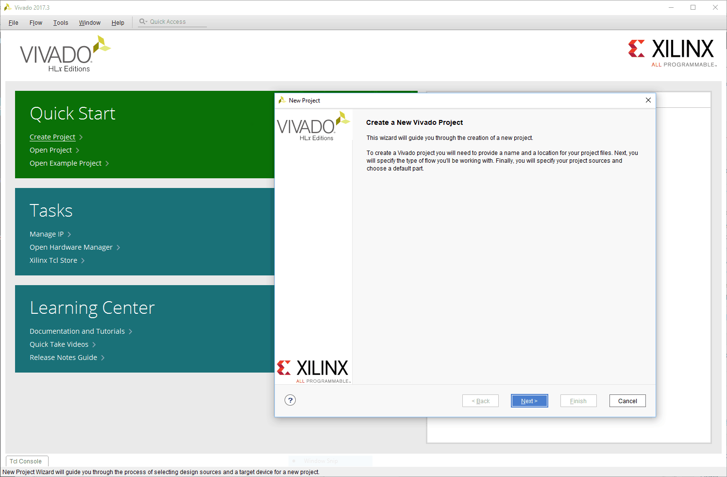
Start Xilinx Vivado Design Suite and select “New Project” from “File” menu. A “New Project” dialog will open. Click “Next” to proceed.
Step 3:
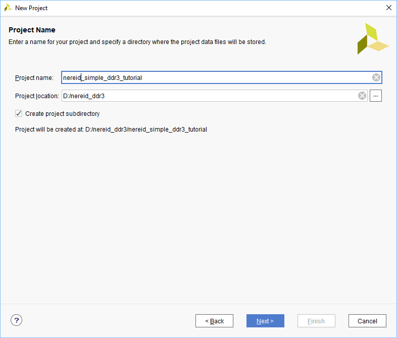
Type in a project name, select a convenient project location and choose “Create project subdirectory” to keep all project files in a single folder. In this article, author has used “nereid-simple-ddr3-tutorial” as a project name. Click “Next”, select “RTL Project” as project type and select “Do not specify sources at this time”. Click “Next” to proceed.
Step 4:
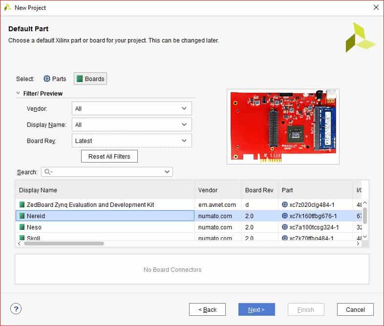
Select “Boards” from “Default Part” tab, choose “numato.com” as a Vendor. Select “Nereid” and click “Next”. If Nereid is not listed, make sure board support files are installed correctly. Click “Finish”. A new Vivado project will open with the selected settings.
Step 5:
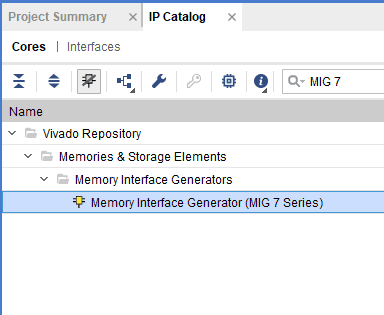
Under the “Flow Navigator”, double click on “IP Catalogue” to add necessary IP cores. Search for MIG 7 and double click on “Memory Interface Generator (MIG 7 Series)” to customise it.
Step 6:
The “Xilinx Memory Interface Generator” configuration window will open. Click “Next”, select component name and de-select “AXI4 Interface”. For this example, “mem” is used as component name. After clicking on “Next” twice, select “DDR3 SDRAM” as Memory. Click “Next”. Click “Create Custom Part” to create custom memory. A dialog will open, enter new memory part name, select base part as “MT8KTF51264HZ-1G9” and use the timing parameters shown below. Click “Save”. 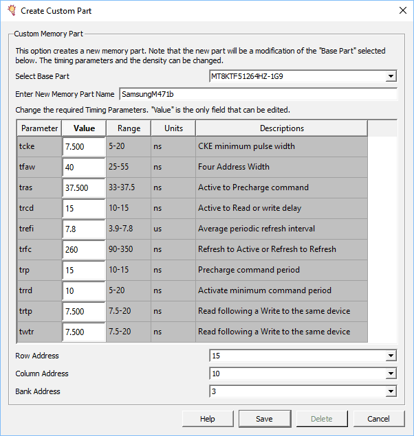
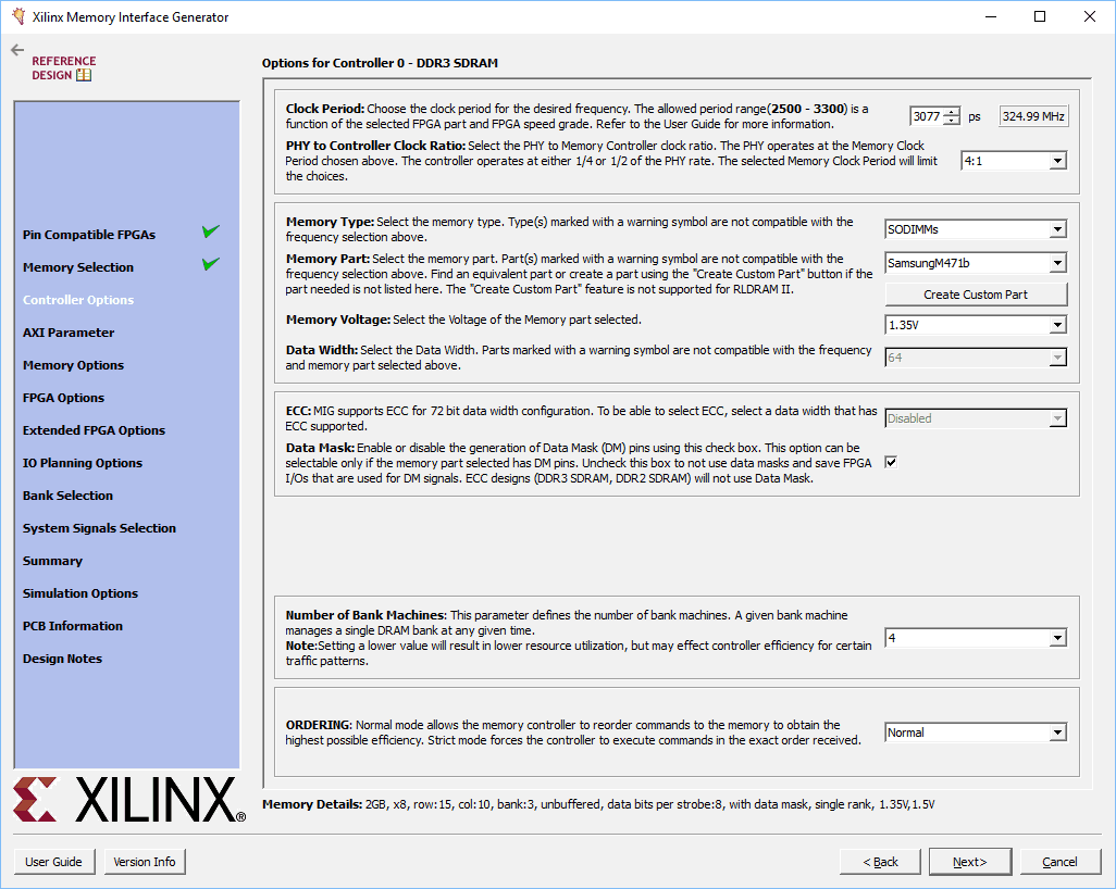
Select the ‘Controller Options’ as shown below and Click “Next”. Select “Input Clock Period” as “5000 ps (200MHz) “, remaining settings are default. Click “Next” to proceed.
Step 7:
Select “FPGA options” as shown below.
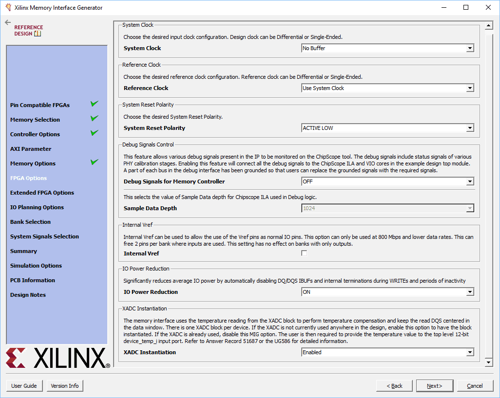
Click Next, choose “Internal Termination Impedance” as “OFF”. Select “Fixed Pin Out” in the next tab and click “Next”. Assign DDR pins as mentioned in nereid constraint file and validate it by clicking “Validate”. If the pinout is valid click “OK” and “Next” to proceed. Accept the license and click “Next” to proceed. Click “Generate” after clicking “Next” to generate IP core with our customised settings.
Step 8:
Search for “Clocking Wizard” IP and double click on it to customise. Choose component name as “clk_wiz”, select “CLK_IN1” board interface to sys_clock and “EXT_RESET_IN” to reset in the “Board” tab. In “Clocking Options” choose primary clock port name as “clk_in”. Choose clk_out1 port name as “clk_200”, requested frequency as “200.000”, de-select locked signal and select “Reset Type” as “Active Low”. Click “OK”.
Step 9 :
Create a verilog file with .v extension and copy paste the following code in “nereid_ddr3.v” to run simple DDR3 with user interface.
The following code uses the clock wizard IP core and Xilinx MIG 7 IP core along with its own logic for interfacing with the MIG 7 IP core. The clock wizard IP core is used to provide the input clock for MIG 7 which is 200MHz, derived from the 100MHz system clock.
The RTL code basically implements a simple FSM with six states to interface with the memory controller. Initially, the FSM is in IDLE state waiting for the memory calibration to complete. When the memory calibration completes successfully, the state machine changes to WRITE state. In WRITE state, the state machine waits for the ready signals from the MIG IP core to accept command and data. Once the app_rdy and app_wdf_rdy signals from the MIG IP go HIGH, the core is ready to accept commands and the data to write to DDR3. The state machine writes data and command to MIG IP core and changes its state to WRITE_DONE. In this state, the command enable (app_en) and data enable (app_wdf_en) are de-asserted by the state machine. Whenever command and data enable signals become LOW, the state proceeds to READ state to read data back from memory. In READ state, state machine waits for the ready signal from MIG IP to accept command. When the app_rdy is asserted from MIG, the command is accepted and the state changes to READ_DONE. In READ_DONE state, the state machine de-asserts the command enable and waits for the app_rd_data_valid to get asserted. Whenever app_rd_data_valid signal gets asserted, the data is read back from memory to data_read_from_memory register and the state changes to PARK. In PARK state, the machine compares the data written to DDR3 with the data read back from DDR3. The RGB LEDs are Active-Low, soled_calib, led_pass and led_fail signals have to be driven low when asserted. If the data match, then led_pass goes LOW otherwise led_fail goes LOW. The memory calibration is inverted and assigned to led_calib.
module nereid_ddr3 (
 input clk_in,

 // DDR3 Physical Interface Signals
 //Inouts
 inout [15:0] ddr3_dq,
 inout [1:0]  ddr3_dqs_n,
 inout [1:0]  ddr3_dqs_p,
 // Outputs
 output [13:0] ddr3_addr,
 output [2:0]  ddr3_ba,
 output ddr3_ras_n,
 output ddr3_cas_n,
 output ddr3_we_n,
 output ddr3_reset_n,
 output [0:0] ddr3_ck_p,
 output [0:0] ddr3_ck_n,
 output [0:0] ddr3_cke,
 output [0:0] ddr3_cs_n,
 output [1:0] ddr3_dm,
 output [0:0] ddr3_odt,

 // LEDs to signal pass/fail
 output reg  led_pass,
 output reg  led_fail,
 output wire led_calib
 );

wire calib_done;

 reg  [27:0] app_addr = 0;
 reg  [2:0]  app_cmd = 0;
 reg  app_en;
 wire app_rdy;

 reg  [127:0] app_wdf_data;
 wire app_wdf_end = 1;
 reg  app_wdf_wren;
 wire app_wdf_rdy;

 wire [127:0] app_rd_data;
 wire [15:0]  app_wdf_mask = 0;
 wire app_rd_data_end;
 wire app_rd_data_valid;

 wire app_sr_req = 0;
 wire app_ref_req = 0;
 wire app_zq_req = 0;
 wire app_sr_active;
 wire app_ref_ack;
 wire app_zq_ack;

 wire ui_clk;
 wire ui_clk_sync_rst;

 wire sys_clk_i;

 reg [127:0] data_to_write = {32'hcafebabe, 32'h12345678,
                              32'hAA55AA55, 32'h55AA55AA};
 reg [127:0] data_read_from_memory = 128'd0;

// Power-on-reset generator circuit.
 // Asserts resetn for 1023 cycles, then deasserts
 // `resetn` is Active low reset
 reg [9:0] por_counter = 1023;
 always @ (posedge clk_in) begin
   if (por_counter) begin
     por_counter <= por_counter - 1 ;
   end
 end

wire resetn = (por_counter == 0);

// Clock Wizard
 // DDR3 core requires 200MHz input clock
 // We generate this clock using Xilinx Clocking Wizard IP Core
 clk_wiz clk_wiz (
   .clk_in  (clk_in),
   .clk_200 (sys_clk_i),
   .resetn  (resetn)
   );

// Instatiation of MIG core named `mem`
 mem mem (
   // DDR3 Physical interface ports
   .ddr3_addr    (ddr3_addr),
   .ddr3_ba      (ddr3_ba),
   .ddr3_cas_n   (ddr3_cas_n),
   .ddr3_ck_n    (ddr3_ck_n),
   .ddr3_ck_p    (ddr3_ck_p),
   .ddr3_cke     (ddr3_cke),
   .ddr3_ras_n   (ddr3_ras_n),
   .ddr3_reset_n (ddr3_reset_n),
   .ddr3_we_n    (ddr3_we_n),
   .ddr3_dq      (ddr3_dq),
   .ddr3_dqs_n   (ddr3_dqs_n),
   .ddr3_dqs_p   (ddr3_dqs_p),
   .ddr3_cs_n    (ddr3_cs_n),
   .ddr3_dm      (ddr3_dm),
   .ddr3_odt     (ddr3_odt),

   .init_calib_complete (calib_done),

   // User interface ports
   .app_addr     (app_addr),
   .app_cmd      (app_cmd),
   .app_en       (app_en),
   .app_wdf_data (app_wdf_data),
   .app_wdf_end  (app_wdf_end),
   .app_wdf_wren (app_wdf_wren),
   .app_rd_data  (app_rd_data),
   .app_rd_data_end (app_rd_data_end),
   .app_rd_data_valid (app_rd_data_valid),
   .app_rdy      (app_rdy),
   .app_wdf_rdy  (app_wdf_rdy),
   .app_sr_req   (app_sr_req),
   .app_ref_req  (app_ref_req),
   .app_zq_req   (app_zq_req),
   .app_sr_active(app_sr_active),
   .app_ref_ack  (app_ref_ack),
   .app_zq_ack   (app_zq_ack),
   .ui_clk       (ui_clk),
   .ui_clk_sync_rst (ui_clk_sync_rst),
   .app_wdf_mask (app_wdf_mask),
   // Clock and Reset input ports
   .sys_clk_i    (sys_clk_i),
   .sys_rst      (resetn)
   );

 localparam IDLE       = 3'd0;
 localparam WRITE      = 3'd1;
 localparam WRITE_DONE = 3'd2;
 localparam READ       = 3'd3;
 localparam READ_DONE  = 3'd4;
 localparam PARK       = 3'd5;
 reg [2:0] state = IDLE;

 localparam CMD_WRITE = 3'b000;
 localparam CMD_READ  = 3'b001;

assign led_calib = ~calib_done;

always @ (posedge ui_clk) begin
  if (ui_clk_sync_rst) begin
    state <= IDLE;
    app_en <= 0;
    app_wdf_wren <= 0;
  end else begin

    case (state)
      IDLE: begin
        if (calib_done) begin
          state <= WRITE;
        end
      end

      WRITE: begin
        if (app_rdy & app_wdf_rdy) begin
          state <= WRITE_DONE;
          app_en <= 1;
          app_wdf_wren <= 1;
          app_addr <= 0;
          app_cmd <= CMD_WRITE;
          app_wdf_data <= data_to_write;
        end
      end

      WRITE_DONE: begin
        if (app_rdy & app_en) begin
          app_en <= 0;
        end

        if (app_wdf_rdy & app_wdf_wren) begin
          app_wdf_wren <= 0;
        end

        if (~app_en & ~app_wdf_wren) begin
          state <= READ;
        end
      end

      READ: begin
        if (app_rdy) begin
          app_en <= 1;
          app_addr <= 0;
          app_cmd <= CMD_READ;
          state <= READ_DONE;
        end
      end

      READ_DONE: begin
        if (app_rdy & app_en) begin
          app_en <= 0;
        end

        if (app_rd_data_valid) begin
          data_read_from_memory <= app_rd_data;
          state <= PARK;
        end
      end

      PARK: begin
        if (data_to_write == data_read_from_memory) begin
          led_pass <= 0;
        end else if (data_to_write != data_read_from_memory) begin
          led_fail <= 0;
        end
      end

      default: state <= IDLE;
    endcase
  end
end

endmodule // nereid_ddr3
Step 10:
Create a constraint file and copy-paste the following constraints.
set_property -dict { PACKAGE_PIN “J26” IOSTANDARD LVCMOS33 SLEW FAST} [get_ports { led_calib }] ;
set_property -dict { PACKAGE_PIN “H26” IOSTANDARD LVCMOS33 SLEW FAST} [get_ports { led_pass }] ;
set_property -dict { PACKAGE_PIN “G26” IOSTANDARD LVCMOS33 SLEW FAST} [get_ports { led_fail }] ;
Step 11:
Generate Bitstream by clicking on “Generate Bitstream”. Once Bitstream generated successfully, power up Nereid and program the device.
If RAM Module inserted,
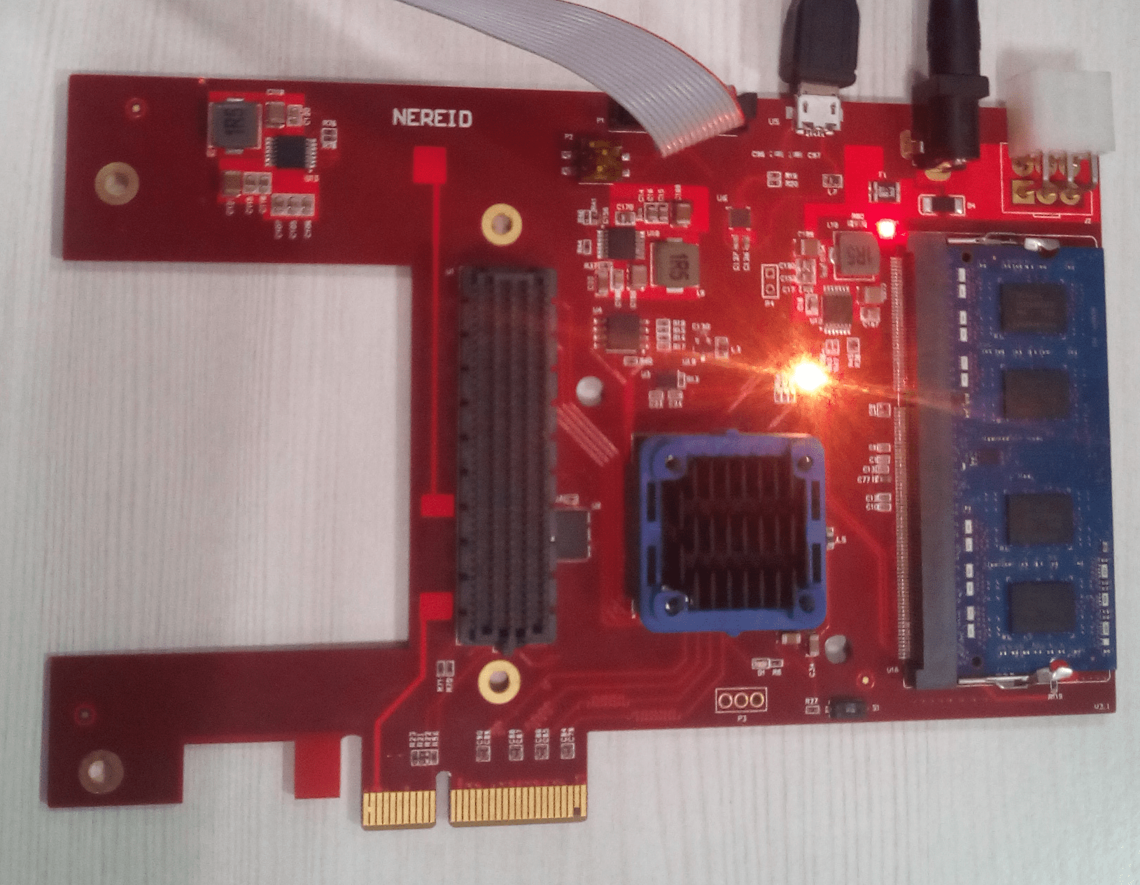
- DDR3 is working properly, Red and Green LEDs both will glow (As a result, combined color will be visible as yellow as shown in image above).
- DDR3 is not working properly, Blue LED will glow.
If RAM Module is not inserted properly, none of the LEDs will glow. If you observe Red and Green LEDs glowing for a while, then your Nereid Kintex 7 DDR3 Example Design worked. Congratulations!
Thank you very much! This was very helpful.
July 19, 2018 at 4:23 am