Introduction
The purpose of this article is to help readers understand how to use DDR3 memory available on Galatea using Xilinx MIG 6 IP core easily. The MIG 6 IP core provides users with two options to interface with memory: User Interface (a wrapper over Native interface) and the AXI4 Interface. This article will demonstrate how to write to the DDR3 memory on Galatea using simple Verilog code and then read back the data. The design will compare the data written to DDR3 and the data read back from it. The verification and DDR3 calibration results are indicated using GPIO pins on Galatea header P4.
Prerequisites
- Hardware:
- Galatea PCI Express Spartan 6 FPGA Development Board
- Xilinx Platform Cable USB II JTAG debugger
- Software:
- Xilinx ISE Design Suite 14.7
Let’s get started
The following steps will walk you through the process of creating a simple DDR3 project using Xilinx ISE Design Suite.
Step 1:
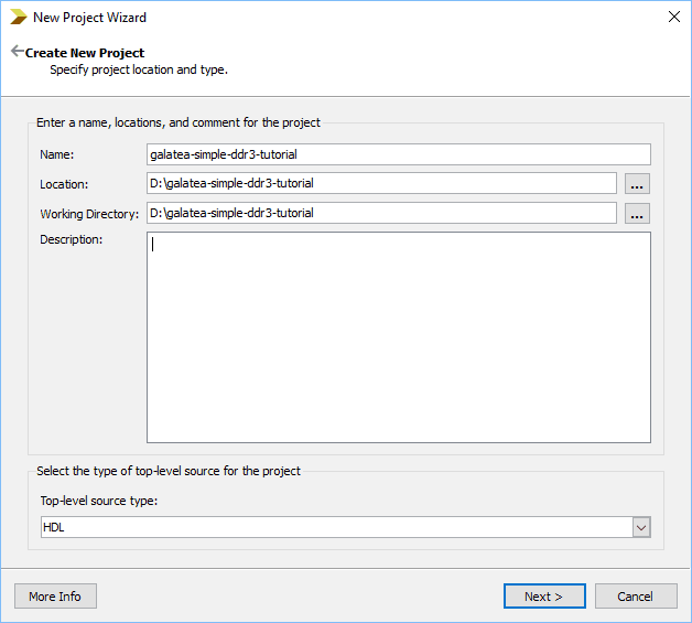
Open Xilinx ISE Design Suite and select “New Project” from “File” menu. The “New Project Wizard” window will open. Type in a project name and select a convenient project location. In this article, author used “galatea-simple-ddr3-tutorial” as the project name. Click “Next” to proceed.
Step 2:
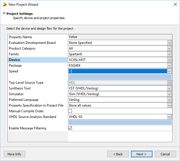
Specify the device and project settings (Family: Spartan 6, Device: XC6SLX45T, Package: FGG484 and Speed grade: -3) in “Project Settings” step as shown below. Click “Next” and “Finish”. A new ISE project will open with the selected settings.
Step 3:
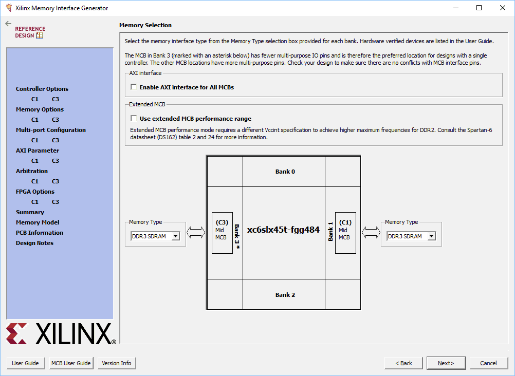
Under “Design” tab, right click and click “New Source”. Select “IP (CORE Generator & Architecture Wizard)”, type “File Name” as “mem” and click “Next” to proceed. Select the “MIG IP” from “Select IP” tab, click “Next” and “Finish”. The “Xilinx Memory Interface Generator” dialog will open. Click “Next” for three consecutive times and select the “Memory Type” as “DDR3 SDRAM” on both banks (1 & 3) as shown below. Galatea features two on-board DDR3 SDRAM memories, one of Bank 1 and the other on Bank 3. As shown below, C3 is controller for Bank 3 and C1 is controller for Bank 1. Click “Next”.
Step 4:
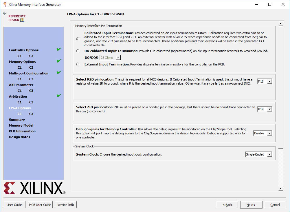
In the “Options for C1”, select “Frequency” as “3000 ps” and “Memory Type” as “MT41J128M16XX-125” . Click “Next” and select the same settings in case of “Options for C3”. Click “Next” and keep the default settings. Again leave the settings to default by clicking on the “Next”. Select Port Configuration for C1 as “one 128-bit bi-directional port”, click “Next” and select the same for C3 Port configuration. Click “Next” further three times. Select the FPGA options for C1 as follows and click “Next” to proceed.
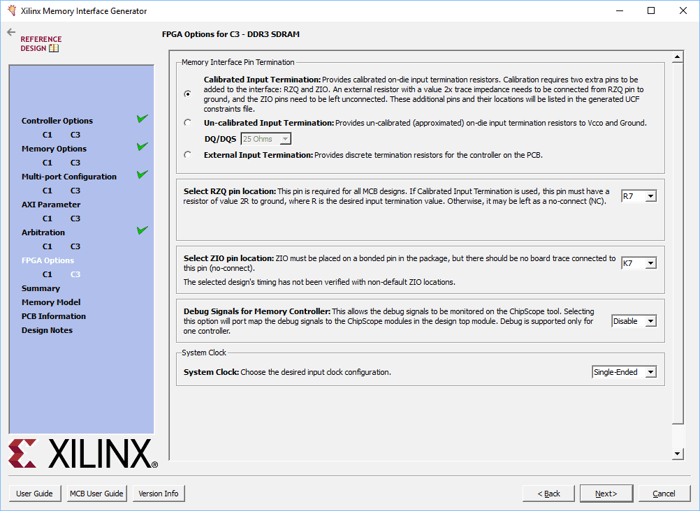
Select the FPGA options for C3 as follows and click “Next” to proceed.
Accept the license by clicking on the “Next” twice. Click “Next” twice and “Generate” to create MIG IP core.
Step 5:
Create a Verilog file with .v extension and copy paste the following code in “galatea_ddr3.v” to run simple DDR3 with the user interface.
The following code uses MIG 6 IP core and the input clock for the MIG is provided by the system clock directly which is 100MHz. The two separate system clocks (100MHz) are provided for two DDR3 memories which are available on Bank 1 and Bank 3 of Galatea.
In the following Verilog code, user design and the MIG IP core are instantiated. The user design is instantiated twice to interface with the two DDR3 memory interface controllers which are C1 (for DDR3 memory available on Bank1) and C3 (for DDR3 memory available on Bank3).
////////////////////////////////////////////////////////////////////
// File Name: galate_ddr3.v
// Description: Instantiation of MIG and user design for C1 and C3
////////////////////////////////////////////////////////////////////
module galatea_ddr3(
 input   c3_sys_clk,
 input   c1_sys_clk,
 input   c_sys_rst_i,
 inout   [15:0] mcb3_dram_dq,
 output  [13:0] mcb3_dram_a,
 output  [2:0]  mcb3_dram_ba,
 output  mcb3_dram_ras_n,
 output  mcb3_dram_cas_n,
 output  mcb3_dram_we_n,
 output  mcb3_dram_odt,
 output  mcb3_dram_reset_n,
 output  mcb3_dram_cke,
 output  mcb3_dram_dm,
 inout   mcb3_dram_udqs,
 inout   mcb3_dram_udqs_n,
 inout   mcb3_rzq,
 inout   mcb3_zio,
 output  mcb3_dram_udm,
 inout   mcb3_dram_dqs,
 inout   mcb3_dram_dqs_n,
 output  mcb3_dram_ck,
 output  mcb3_dram_ck_n,

 inout   [15:0] mcb1_dram_dq,
 output  [13:0] mcb1_dram_a,
 output  [2:0] mcb1_dram_ba,
 output  mcb1_dram_ras_n,
 output  mcb1_dram_cas_n,
 output  mcb1_dram_we_n,
 output  mcb1_dram_odt,
 output  mcb1_dram_reset_n,
 output  mcb1_dram_cke,
 output  mcb1_dram_dm,
 inout   mcb1_dram_udqs,
 inout   mcb1_dram_udqs_n,
 inout   mcb1_rzq,
 inout   mcb1_zio,
 output  mcb1_dram_udm,
 inout   mcb1_dram_dqs,
 inout   mcb1_dram_dqs_n,
 output  mcb1_dram_ck,
 output  mcb1_dram_ck_n,

 output  led1_calib,
 output  led1_pass,
 output  led1_fail,
 output  led3_calib,
 output  led3_pass,
 output  led3_fail
 );

 // Command Signals
 wire [2:0]  c3_p0_cmd_instr;
 wire [5:0]  c3_p0_cmd_bl;
 wire [29:0] c3_p0_cmd_byte_addr;
 wire [2:0]  c1_p0_cmd_instr;
 wire [5:0]  c1_p0_cmd_bl;
 wire [29:0] c1_p0_cmd_byte_addr;
 // Write Signals
 wire [15:0] c3_p0_wr_mask;
 wire [127:0]c3_p0_wr_data;
 wire [6:0]  c3_p0_wr_count;
 wire [15:0] c1_p0_wr_mask;
 wire [127:0]c1_p0_wr_data;
 wire [6:0]  c1_p0_wr_count;
 // Read Signals
 wire [127:0]c3_p0_rd_data;
 wire [6:0]  c3_p0_rd_count;
 wire [127:0]c1_p0_rd_data;
 wire [6:0]  c1_p0_rd_count;

// Instantiation of memory
 mem u_mem (
   .c3_sys_clk        (c3_sys_clk),
   .c3_sys_rst_i      (c_sys_rst_i),

   .mcb3_dram_dq      (mcb3_dram_dq),
   .mcb3_dram_a       (mcb3_dram_a),
   .mcb3_dram_ba      (mcb3_dram_ba),
   .mcb3_dram_ras_n   (mcb3_dram_ras_n),
   .mcb3_dram_cas_n   (mcb3_dram_cas_n),
   .mcb3_dram_we_n    (mcb3_dram_we_n),
   .mcb3_dram_odt     (mcb3_dram_odt),
   .mcb3_dram_cke     (mcb3_dram_cke),
   .mcb3_dram_ck      (mcb3_dram_ck),
   .mcb3_dram_ck_n    (mcb3_dram_ck_n),
   .mcb3_dram_dqs     (mcb3_dram_dqs),
   .mcb3_dram_dqs_n   (mcb3_dram_dqs_n),
   .mcb3_dram_udqs    (mcb3_dram_udqs),   // for X16 parts
   .mcb3_dram_udqs_n  (mcb3_dram_udqs_n), // for X16 parts
   .mcb3_dram_udm     (mcb3_dram_udm), // for X16 parts
   .mcb3_dram_dm      (mcb3_dram_dm),
   .mcb3_dram_reset_n (mcb3_dram_reset_n),
   .c3_clk0           (c3_clk0),
   .c3_rst0           (c3_rst0),
   .c3_calib_done     (led3_calib),
   .mcb3_rzq          (mcb3_rzq),
   .mcb3_zio          (mcb3_zio),
   .c3_p0_cmd_clk     (c3_p0_cmd_clk),
   .c3_p0_cmd_en      (c3_p0_cmd_en),
   .c3_p0_cmd_instr   (c3_p0_cmd_instr),
   .c3_p0_cmd_bl      (c3_p0_cmd_bl),
   .c3_p0_cmd_byte_addr(c3_p0_cmd_byte_addr),
   .c3_p0_cmd_empty   (c3_p0_cmd_empty),
   .c3_p0_cmd_full    (c3_p0_cmd_full),
   .c3_p0_wr_clk      (c3_p0_wr_clk),
   .c3_p0_wr_en       (c3_p0_wr_en),
   .c3_p0_wr_mask     (c3_p0_wr_mask),
   .c3_p0_wr_data     (c3_p0_wr_data),
   .c3_p0_wr_full     (c3_p0_wr_full),
   .c3_p0_wr_empty    (c3_p0_wr_empty),
   .c3_p0_wr_count    (c3_p0_wr_count),
   .c3_p0_wr_underrun (c3_p0_wr_underrun),
   .c3_p0_wr_error    (c3_p0_wr_error),
   .c3_p0_rd_clk      (c3_p0_rd_clk),
   .c3_p0_rd_en       (c3_p0_rd_en),
   .c3_p0_rd_data     (c3_p0_rd_data),
   .c3_p0_rd_full     (c3_p0_rd_full),
   .c3_p0_rd_empty    (c3_p0_rd_empty),
   .c3_p0_rd_count    (c3_p0_rd_count),
   .c3_p0_rd_overflow (c3_p0_rd_overflow),
   .c3_p0_rd_error    (c3_p0_rd_error),

   .c1_sys_clk        (c1_sys_clk),
   .c1_sys_rst_i      (c_sys_rst_i),

   .mcb1_dram_dq      (mcb1_dram_dq),
   .mcb1_dram_a       (mcb1_dram_a),
   .mcb1_dram_ba      (mcb1_dram_ba),
   .mcb1_dram_ras_n   (mcb1_dram_ras_n),
   .mcb1_dram_cas_n   (mcb1_dram_cas_n),
   .mcb1_dram_we_n    (mcb1_dram_we_n),
   .mcb1_dram_odt     (mcb1_dram_odt),
   .mcb1_dram_cke     (mcb1_dram_cke),
   .mcb1_dram_ck      (mcb1_dram_ck),
   .mcb1_dram_ck_n    (mcb1_dram_ck_n),
   .mcb1_dram_dqs     (mcb1_dram_dqs),
   .mcb1_dram_dqs_n   (mcb1_dram_dqs_n),
   .mcb1_dram_udqs    (mcb1_dram_udqs), // for X16 parts
   .mcb1_dram_udqs_n  (mcb1_dram_udqs_n), // for X16 parts
   .mcb1_dram_udm     (mcb1_dram_udm), // for X16 parts
   .mcb1_dram_dm      (mcb1_dram_dm),
   .mcb1_dram_reset_n (mcb1_dram_reset_n),
   .c1_clk0           (c1_clk0),
   .c1_rst0           (c1_rst0),
   .c1_calib_done     (led1_calib),
   .mcb1_rzq          (mcb1_rzq),
   .mcb1_zio          (mcb1_zio),
   .c1_p0_cmd_clk     (c1_p0_cmd_clk),
   .c1_p0_cmd_en      (c1_p0_cmd_en),
   .c1_p0_cmd_instr   (c1_p0_cmd_instr),
   .c1_p0_cmd_bl      (c1_p0_cmd_bl),
   .c1_p0_cmd_byte_addr (c1_p0_cmd_byte_addr),
   .c1_p0_cmd_empty   (c1_p0_cmd_empty),
   .c1_p0_cmd_full    (c1_p0_cmd_full),
   .c1_p0_wr_clk      (c1_p0_wr_clk),
   .c1_p0_wr_en       (c1_p0_wr_en),
   .c1_p0_wr_mask     (c1_p0_wr_mask),
   .c1_p0_wr_data     (c1_p0_wr_data),
   .c1_p0_wr_full     (c1_p0_wr_full),
   .c1_p0_wr_empty    (c1_p0_wr_empty),
   .c1_p0_wr_count    (c1_p0_wr_count),
   .c1_p0_wr_underrun (c1_p0_wr_underrun),
   .c1_p0_wr_error    (c1_p0_wr_error),
   .c1_p0_rd_clk      (c1_p0_rd_clk),
   .c1_p0_rd_en       (c1_p0_rd_en),
   .c1_p0_rd_data     (c1_p0_rd_data),
   .c1_p0_rd_full     (c1_p0_rd_full),
   .c1_p0_rd_empty    (c1_p0_rd_empty),
   .c1_p0_rd_count    (c1_p0_rd_count),
   .c1_p0_rd_overflow (c1_p0_rd_overflow),
   .c1_p0_rd_error    (c1_p0_rd_error)
 );

// Uer Interface instantiation for Bank1 DDR3
galatea_ui ui_c1 (
   .c_clk0            (c1_clk0),
   .c_rst0            (c1_rst0),
   .c_p0_cmd_clk      (c1_p0_cmd_clk),
   .c_p0_cmd_en       (c1_p0_cmd_en),
   .c_p0_cmd_instr    (c1_p0_cmd_instr),
   .c_p0_cmd_bl       (c1_p0_cmd_bl),
   .c_p0_cmd_byte_addr(c1_p0_cmd_byte_addr),
   .c_p0_cmd_empty    (c1_p0_cmd_empty),
   .c_p0_cmd_full     (c1_p0_cmd_full),
   .c_p0_wr_clk       (c1_p0_wr_clk),
   .c_p0_wr_en        (c1_p0_wr_en),
   .c_p0_wr_mask      (c1_p0_wr_mask),
   .c_p0_wr_data      (c1_p0_wr_data),
   .c_p0_wr_full      (c1_p0_wr_full),
   .c_p0_wr_empty     (c1_p0_wr_empty),
   .c_p0_wr_count     (c1_p0_wr_count),
   .c_p0_wr_underrun  (c1_p0_wr_underrun),
   .c_p0_wr_error     (c1_p0_wr_error),
   .c_p0_rd_clk       (c1_p0_rd_clk),
   .c_p0_rd_en        (c1_p0_rd_en),
   .c_p0_rd_data      (c1_p0_rd_data),
   .c_p0_rd_full      (c1_p0_rd_full),
   .c_p0_rd_empty     (c1_p0_rd_empty),
   .c_p0_rd_count     (c1_p0_rd_count),
   .c_p0_rd_overflow  (c1_p0_rd_overflow),
   .c_p0_rd_error     (c1_p0_rd_error),
   .led_calib         (led1_calib),
   .led_pass          (led1_pass),
   .led_fail          (led1_fail)
   );

// Uer Interface instantiation for Bank3 DDR3
galatea_ui ui_c3 (
   .c_clk0            (c3_clk0),
   .c_rst0            (c3_rst0),
   .c_p0_cmd_clk      (c3_p0_cmd_clk),
   .c_p0_cmd_en       (c3_p0_cmd_en),
   .c_p0_cmd_instr    (c3_p0_cmd_instr),
   .c_p0_cmd_bl       (c3_p0_cmd_bl),
   .c_p0_cmd_byte_addr(c3_p0_cmd_byte_addr),
   .c_p0_cmd_empty    (c3_p0_cmd_empty),
   .c_p0_cmd_full     (c3_p0_cmd_full),
   .c_p0_wr_clk       (c3_p0_wr_clk),
   .c_p0_wr_en        (c3_p0_wr_en),
   .c_p0_wr_mask      (c3_p0_wr_mask),
   .c_p0_wr_data      (c3_p0_wr_data),
   .c_p0_wr_full      (c3_p0_wr_full),
   .c_p0_wr_empty     (c3_p0_wr_empty),
   .c_p0_wr_count     (c3_p0_wr_count),
   .c_p0_wr_underrun  (c3_p0_wr_underrun),
   .c_p0_wr_error     (c3_p0_wr_error),
   .c_p0_rd_clk       (c3_p0_rd_clk),
   .c_p0_rd_en        (c3_p0_rd_en),
   .c_p0_rd_data      (c3_p0_rd_data),
   .c_p0_rd_full      (c3_p0_rd_full),
   .c_p0_rd_empty     (c3_p0_rd_empty),
   .c_p0_rd_count     (c3_p0_rd_count),
   .c_p0_rd_overflow  (c3_p0_rd_overflow),
   .c_p0_rd_error     (c3_p0_rd_error),
   .led_calib         (led3_calib),
   .led_pass          (led3_pass),
   .led_fail          (led3_fail)
   );
endmodule //galatea_ddr3
Create a Verilog file with .v extension and copy paste the following code in “galatea_ui.v”
In the following RTL code, a simple FSM is implemented with six states. The six states are IDLE, WR_CMD, WRITE, RD_CMD, READ and PARK.
Initially, the state machine is in the IDLE state. In this state, the FSM waits for the calibration (led_calib) to complete. Once the calibration completes, the state machine changes to WR_CMD state.
In WR_CMD state, the state machine waits for the MIG controller to be ready to accept new commands by checking whether the signal c_p0_cmd_full is deasserted. Once the controller is ready to accept the command, the state machine writes the command to the controller and changes its state to WRITE.
In WRITE state, the FSM de-asserts the command enable and waits for the controller to be ready to accept data to be written to DDR3 by checking whether c_p0_wr_full signal is de-asserted. Once c_p0_wr_full signal is de-asserted, the MIG controller is ready to accept new data to be written to DDR3. The state machine asserts the write enable (c_p0_wr_en) and writes a fixed data (stored in data_to_write register) to controller’s write FIFO. The machine proceeds to RD_CMD state to read back the data from memory.
In RD_CMD state, the state machine waits for the MIG controller to be ready to accept new commands by checking whether the signal c_p0_cmd_full is deasserted, similar to as in WR_CMD state. Whenever the MIG de-asserts the c_p0_cmd_full signal, it is ready to accept the read command. The state machine de-asserts the write enable signal (c_p0_wr_en), writes the “read” command to the MIG IP and changes its state to READ state.
In READ state, the FSM de-asserts the command enable (c_p0_cmd_en) and waits for the read empty signal (c_p0_rd_empty) from MIG to go low. Once the read empty signal gets de-asserted by MIG, the state machine captures data from MIG’s FIFO to data_read_from_memory register and changes its state to PARK.
The PARK state is used to compare the data written to the memory with the data read back from memory. If both match, then led_pass goes HIGH otherwise led_fail goes HIGH.
////////////////////////////////////////////////////////////////////////////
// File Name: galatea_ui
// Description: Simple FSM to write data to memory and read back from it
////////////////////////////////////////////////////////////////////////////
module galatea_ui(
 input   c_clk0,
 input   c_rst0,
 // Command Signals
 output  c_p0_cmd_clk,
 output  reg c_p0_cmd_en,
 output  reg [2:0]  c_p0_cmd_instr,
 output  reg [5:0]  c_p0_cmd_bl,
 output  reg [29:0] c_p0_cmd_byte_addr,
 input   c_p0_cmd_empty,
 input   c_p0_cmd_full,
 // Write Signals
 output  c_p0_wr_clk,
 output  reg c_p0_wr_en,
 output  [15:0] c_p0_wr_mask,
 output  reg [127:0]c_p0_wr_data,
 input   c_p0_wr_full,
 input   c_p0_wr_empty,
 input   [6:0] c_p0_wr_count,
 input   c_p0_wr_underrun,
 input   c_p0_wr_error,
 // Read Signals
 output  c_p0_rd_clk,
 output  reg c_p0_rd_en,
 input   [127:0]c_p0_rd_data,
 input   c_p0_rd_full,
 input   c_p0_rd_empty,
 input   [6:0]  c_p0_rd_count,
 input   c_p0_rd_overflow,
 input   c_p0_rd_error,
 input   led_calib,
 output  reg led_pass,
 output  reg led_fail
 );

reg  [2:0]  state;
reg  [127:0]data_read_from_memory = 128'd0;
wire [127:0]data_to_write = {32'hcafebabe, 32'h12345678,
                             32'hAA55AA55, 32'h55AA55AA};

assign c_p0_cmd_clk = c_clk0;
assign c_p0_wr_clk  = c_clk0;
assign c_p0_rd_clk  = c_clk0;

localparam IDLE   = 3'h0,
           WR_CMD = 3'h1,
           WRITE  = 3'h2,
           RD_CMD = 3'h3,
           READ   = 3'h4,
           PARK   = 3'h5;
assign c_p0_wr_mask = 16'h0000;
//****************** State Machine start here ****************************//
always@(posedge c_clk0)
begin
  if(c_rst0) begin
    c_p0_cmd_byte_addr <= 0;
    c_p0_cmd_bl   <= 1;
    state         <= IDLE;
    c_p0_cmd_instr<= 3'b000;
    c_p0_cmd_en   <= 1'b0;
    c_p0_wr_en    <= 1'b0;
    c_p0_rd_en    <= 1'b0;
    led_pass      <= 1'b0;
    led_fail      <= 1'b0;
   end
   else begin
     case(state)
       IDLE : begin
         if(led_calib) begin
           state <= WR_CMD;
         end
       end

       WR_CMD : begin
         if(~c_p0_cmd_full) begin
           c_p0_cmd_byte_addr <= 0;
           c_p0_cmd_bl    <= 1;
           c_p0_cmd_instr <= 3'b000;
           c_p0_cmd_en    <= 1'b1;
           state          <= WRITE;
          end
       end

       WRITE : begin
         c_p0_cmd_en    <= 1'b0;
         if(~c_p0_wr_full) begin
           c_p0_wr_en   <= 1'b1;
           c_p0_wr_data <= data_to_write;
           state        <= RD_CMD;
         end
       end

       RD_CMD : begin
         if(~c_p0_cmd_full) begin
           c_p0_wr_en     <= 1'b0;
           c_p0_cmd_byte_addr <= 0;
           c_p0_cmd_bl    <= 1;
           c_p0_cmd_instr <= 3'b001;
           c_p0_cmd_en    <= 1'b1;
           state          <= READ;
         end
       end

       READ : begin
         c_p0_cmd_en  <= 1'b0;
         if(~c_p0_rd_empty) begin
           c_p0_rd_en <= 1'b1;
           data_read_from_memory <= c_p0_rd_data;
           state      <= PARK;
         end
       end

       PARK : begin
         c_p0_rd_en <= 1'b0;
         if (data_to_write == data_read_from_memory) begin
           led_pass <= 1;
         end else if (data_to_write != data_read_from_memory) begin
           led_fail <= 1;
         end
       end

       default: state <= IDLE;
     endcase
   end
end
endmodule
Step 6:
Create a constraints file and copy-paste the following constraints.
CONFIG VCCAUX = "3.3" ;

NET "c3_sys_clk"  LOC = G9  | IOSTANDARD = LVCMOS33 | PERIOD = 100MHz;
NET "c1_sys_clk"  LOC = Y13 | IOSTANDARD = LVCMOS33 | PERIOD = 100MHz;
NET "c_sys_rst_i" LOC = G11 | IOSTANDARD = LVCMOS33 | DRIVE = 8 | SLEW = FAST | PULLDOWN;

NET "led3_fail"   LOC = B18 | IOSTANDARD = LVCMOS33 | DRIVE = 8 | SLEW = FAST;
NET "led3_pass"   LOC = D19 | IOSTANDARD = LVCMOS33 | DRIVE = 8 | SLEW = FAST;
NET "led3_calib"  LOC = D18 | IOSTANDARD = LVCMOS33 | DRIVE = 8 | SLEW = FAST;

NET "led1_fail"   LOC = A19 | IOSTANDARD = LVCMOS33 | DRIVE = 8 | SLEW = FAST;
NET "led1_pass"   LOC = C19 | IOSTANDARD = LVCMOS33 | DRIVE = 8 | SLEW = FAST;
NET "led1_calib"  LOC = A18 | IOSTANDARD = LVCMOS33 | DRIVE = 8 | SLEW = FAST;

NET "mcb3_dram_a[0]"    LOC = "K2" | IOSTANDARD = SSTL15_II;
NET "mcb3_dram_a[1]"    LOC = "K1" | IOSTANDARD = SSTL15_II;
NET "mcb3_dram_a[2]"    LOC = "K5" | IOSTANDARD = SSTL15_II;
NET "mcb3_dram_a[3]"    LOC = "M6" | IOSTANDARD = SSTL15_II;
NET "mcb3_dram_a[4]"    LOC = "H3" | IOSTANDARD = SSTL15_II;
NET "mcb3_dram_a[5]"    LOC = "M3" | IOSTANDARD = SSTL15_II;
NET "mcb3_dram_a[6]"    LOC = "L4" | IOSTANDARD = SSTL15_II;
NET "mcb3_dram_a[7]"    LOC = "K6" | IOSTANDARD = SSTL15_II;
NET "mcb3_dram_a[8]"    LOC = "G3" | IOSTANDARD = SSTL15_II;
NET "mcb3_dram_a[9]"    LOC = "G1" | IOSTANDARD = SSTL15_II;
NET "mcb3_dram_a[10]"   LOC = "J4" | IOSTANDARD = SSTL15_II;
NET "mcb3_dram_a[11]"   LOC = "E1" | IOSTANDARD = SSTL15_II;
NET "mcb3_dram_a[12]"   LOC = "F1" | IOSTANDARD = SSTL15_II;
NET "mcb3_dram_a[13]"   LOC = "J6" | IOSTANDARD = SSTL15_II;

NET "mcb3_dram_dq[0]"   LOC = "R3" | IOSTANDARD = SSTL15_II;
NET "mcb3_dram_dq[1]"   LOC = "R1" | IOSTANDARD = SSTL15_II;
NET "mcb3_dram_dq[2]"   LOC = "P2" | IOSTANDARD = SSTL15_II;
NET "mcb3_dram_dq[3]"   LOC = "P1" | IOSTANDARD = SSTL15_II;
NET "mcb3_dram_dq[4]"   LOC = "L3" | IOSTANDARD = SSTL15_II;
NET "mcb3_dram_dq[5]"   LOC = "L1" | IOSTANDARD = SSTL15_II;
NET "mcb3_dram_dq[6]"   LOC = "M2" | IOSTANDARD = SSTL15_II;
NET "mcb3_dram_dq[7]"   LOC = "M1" | IOSTANDARD = SSTL15_II;
NET "mcb3_dram_dq[8]"   LOC = "T2" | IOSTANDARD = SSTL15_II;
NET "mcb3_dram_dq[9]"   LOC = "T1" | IOSTANDARD = SSTL15_II;
NET "mcb3_dram_dq[10]"  LOC = "U3" | IOSTANDARD = SSTL15_II;
NET "mcb3_dram_dq[11]"  LOC = "U1" | IOSTANDARD = SSTL15_II;
NET "mcb3_dram_dq[12]"  LOC = "W3" | IOSTANDARD = SSTL15_II;
NET "mcb3_dram_dq[13]"  LOC = "W1" | IOSTANDARD = SSTL15_II;
NET "mcb3_dram_dq[14]"  LOC = "Y2" | IOSTANDARD = SSTL15_II;
NET "mcb3_dram_dq[15]"  LOC = "Y1" | IOSTANDARD = SSTL15_II;

NET "mcb3_dram_ba[0]"   LOC = "J3" | IOSTANDARD = SSTL15_II;
NET "mcb3_dram_ba[1]"   LOC = "J1" | IOSTANDARD = SSTL15_II;
NET "mcb3_dram_ba[2]"   LOC = "H1" | IOSTANDARD = SSTL15_II;
NET "mcb3_dram_ras_n"   LOC = "M5" | IOSTANDARD = SSTL15_II;
NET "mcb3_dram_cas_n"   LOC = "M4" | IOSTANDARD = SSTL15_II;
NET "mcb3_dram_we_n"    LOC = "H2" | IOSTANDARD = SSTL15_II;
NET "mcb3_dram_ck"      LOC = "K4" | IOSTANDARD = DIFF_SSTL15_II;
NET "mcb3_dram_ck_n"    LOC = "K3" | IOSTANDARD = DIFF_SSTL15_II;
NET "mcb3_dram_cke"     LOC = "F2" | IOSTANDARD = SSTL15_II;
NET "mcb3_dram_dm"      LOC = "N4" | IOSTANDARD = SSTL15_II;
NET "mcb3_dram_dqs"     LOC = "N3" | IOSTANDARD = DIFF_SSTL15_II;
NET "mcb3_dram_dqs_n"   LOC = "N1" | IOSTANDARD = DIFF_SSTL15_II;
NET "mcb3_dram_udqs"    LOC = "V2" | IOSTANDARD = DIFF_SSTL15_II;
NET "mcb3_dram_udqs_n"  LOC = "V1" | IOSTANDARD = DIFF_SSTL15_II;
NET "mcb3_dram_udm"     LOC = "P3" | IOSTANDARD = SSTL15_II;
NET "mcb3_dram_odt"     LOC = "L6" | IOSTANDARD = SSTL15_II;
NET "mcb3_dram_reset_n" LOC = "E3" | IOSTANDARD = LVCMOS15;
NET "mcb3_zio" IOSTANDARD = SSTL15_II;
NET "mcb3_rzq" IOSTANDARD = SSTL15_II;

NET "mcb1_dram_a[0]"    LOC = "H21" | IOSTANDARD = SSTL15_II;
NET "mcb1_dram_a[1]"    LOC = "H22" | IOSTANDARD = SSTL15_II;
NET "mcb1_dram_a[2]"    LOC = "G22" | IOSTANDARD = SSTL15_II;
NET "mcb1_dram_a[3]"    LOC = "J20" | IOSTANDARD = SSTL15_II;
NET "mcb1_dram_a[4]"    LOC = "H20" | IOSTANDARD = SSTL15_II;
NET "mcb1_dram_a[5]"    LOC = "M20" | IOSTANDARD = SSTL15_II;
NET "mcb1_dram_a[6]"    LOC = "M19" | IOSTANDARD = SSTL15_II;
NET "mcb1_dram_a[7]"    LOC = "G20" | IOSTANDARD = SSTL15_II;
NET "mcb1_dram_a[8]"    LOC = "E20" | IOSTANDARD = SSTL15_II;
NET "mcb1_dram_a[9]"    LOC = "E22" | IOSTANDARD = SSTL15_II;
NET "mcb1_dram_a[10]"   LOC = "J19" | IOSTANDARD = SSTL15_II;
NET "mcb1_dram_a[11]"   LOC = "H19" | IOSTANDARD = SSTL15_II;
NET "mcb1_dram_a[12]"   LOC = "F22" | IOSTANDARD = SSTL15_II;
NET "mcb1_dram_a[13]"   LOC = "G19" | IOSTANDARD = SSTL15_II;

NET "mcb1_dram_dq[0]"   LOC = "R20" | IOSTANDARD = SSTL15_II;
NET "mcb1_dram_dq[1]"   LOC = "R22" | IOSTANDARD = SSTL15_II;
NET "mcb1_dram_dq[2]"   LOC = "P21" | IOSTANDARD = SSTL15_II;
NET "mcb1_dram_dq[3]"   LOC = "P22" | IOSTANDARD = SSTL15_II;
NET "mcb1_dram_dq[4]"   LOC = "L20" | IOSTANDARD = SSTL15_II;
NET "mcb1_dram_dq[5]"   LOC = "L22" | IOSTANDARD = SSTL15_II;
NET "mcb1_dram_dq[6]"   LOC = "M21" | IOSTANDARD = SSTL15_II;
NET "mcb1_dram_dq[7]"   LOC = "M22" | IOSTANDARD = SSTL15_II;
NET "mcb1_dram_dq[8]"   LOC = "T21" | IOSTANDARD = SSTL15_II;
NET "mcb1_dram_dq[9]"   LOC = "T22" | IOSTANDARD = SSTL15_II;
NET "mcb1_dram_dq[10]"  LOC = "U20" | IOSTANDARD = SSTL15_II;
NET "mcb1_dram_dq[11]"  LOC = "U22" | IOSTANDARD = SSTL15_II;
NET "mcb1_dram_dq[12]"  LOC = "W20" | IOSTANDARD = SSTL15_II;
NET "mcb1_dram_dq[13]"  LOC = "W22" | IOSTANDARD = SSTL15_II;
NET "mcb1_dram_dq[14]"  LOC = "Y21" | IOSTANDARD = SSTL15_II;
NET "mcb1_dram_dq[15]"  LOC = "Y22" | IOSTANDARD = SSTL15_II;

NET "mcb1_dram_ba[0]"   LOC = "K17" | IOSTANDARD = SSTL15_II;
NET "mcb1_dram_ba[1]"   LOC = "L17" | IOSTANDARD = SSTL15_II;
NET "mcb1_dram_ba[2]"   LOC = "K18" | IOSTANDARD = SSTL15_II;
NET "mcb1_dram_ras_n"   LOC = "K21" | IOSTANDARD = SSTL15_II;
NET "mcb1_dram_cas_n"   LOC = "K22" | IOSTANDARD = SSTL15_II;
NET "mcb1_dram_we_n"    LOC = "K19" | IOSTANDARD = SSTL15_II;
NET "mcb1_dram_ck"      LOC = "K20" | IOSTANDARD = DIFF_SSTL15_II;
NET "mcb1_dram_ck_n"    LOC = "L19" | IOSTANDARD = DIFF_SSTL15_II;
NET "mcb1_dram_cke"     LOC = "F21" | IOSTANDARD = SSTL15_II;
NET "mcb1_dram_dm"      LOC = "N19" | IOSTANDARD = SSTL15_II;
NET "mcb1_dram_dqs"     LOC = "N20" | IOSTANDARD = DIFF_SSTL15_II;
NET "mcb1_dram_dqs_n"   LOC = "N22" | IOSTANDARD = DIFF_SSTL15_II;
NET "mcb1_dram_udqs"    LOC = "V21" | IOSTANDARD = DIFF_SSTL15_II;
NET "mcb1_dram_udqs_n"  LOC = "V22" | IOSTANDARD = DIFF_SSTL15_II;
NET "mcb1_dram_udm"     LOC = "P20" | IOSTANDARD = SSTL15_II;
NET "mcb1_dram_odt"     LOC = "J22" | IOSTANDARD = SSTL15_II;
NET "mcb1_dram_reset_n" LOC = "H18" | IOSTANDARD = LVCMOS15;
NET "mcb1_zio" IOSTANDARD = SSTL15_II;
NET "mcb1_rzq" IOSTANDARD = SSTL15_II;
Step 7:
Generate Bitstream by clicking on “Generate Bitstream”. Once the Bitstream is generated successfully, power up Galatea and program it using Xilinx Platform Cable USB II.
FPGA pins A18, C19 and A19 are connected to led_calib1, led_pass1 and led_fail1 signals respectively, corresponding to controller C1 for DRR3 on Bank 1. FPGA pins D18, D19 and B18 are connected to led_calib3, led_pass3 and led_fail3 respectively, corresponding to controller C3 for DRR3 on Bank 3. After programming make sure that led_calib1 and led_calib3 (calibration done) signals go HIGH indicating that initial calibration completed successfully for both DDR3 memories which are available on Bank 1 and Bank 3 of the FPGA. Also, led_pass1 and led_pass3 should go HIGH indicating that data written to memory and read back successfully and led_fail1 and led_fail3 should stay LOW since led_fail1 and led_fail3 being HIGH indicates failed attempt to write to and read data from memory.
You can use either LED and resistor or Multimeter to measure the output of these signals. If you observe led_calib1, led_calib3, led_pass1 and led_pass3 LEDs high and led_fail1and led_fail3 LEDs stay low, then your Galatea PCI Express Spartan 6 DDR3 example design worked. Congratulations!