Introduction:
Ethernet is a Link Layer Protocol in the TCP/IP protocol stack between the physical and data link layer. It is the most widely used protocol for Local Area Networks (LANs). Every device on Ethernet is assigned a unique MAC address for communication. Gigabit Ethernet refers to various technologies developed for transmitting Ethernet frames at the rate of gigabits per second. The Reduced Gigabit Media-Independent Interface (RGMII) is used to interface the Ethernet IP core on FPGA with the Gigabit Ethernet PHY chip (RTL8211E) on Mimas A7. The Media Access Layer converts the packets into a stream of data to be sent while the Physical Layer converts the stream of data into electrical signals. RGMII provides a media-independent interface so that MAC and PHY can be compatible, irrespective of the hardware used. In this tutorial, the Numato Lab Mimas A7 FPGA Development Board is used to demonstrate a TCP/IP echo server application. The echo server application runs on lightweight IP (lwIP) TCP/IP stack.
Prerequisites:
-
Hardware:
- Mimas A7 FPGA Development Board
- Cat 6 Ethernet Cable
- Xilinx Platform Cable USB II JTAG
- USB 2.0 B-type cable
- 5V-12V DC Power Supply
-
Software:
- Xilinx Vivado Design Suite 2023.2.1
- Telnet Application
- Serial Terminal (PuTTY, Tera Term, etc.)
Let’s get Started
Step 1:
Download and install Vivado Board Support Package files for Mimas A7 from here.
Step 2:
Open Vivado Design Suite, go to File->Project->New. The New Project window will open. Click Next.
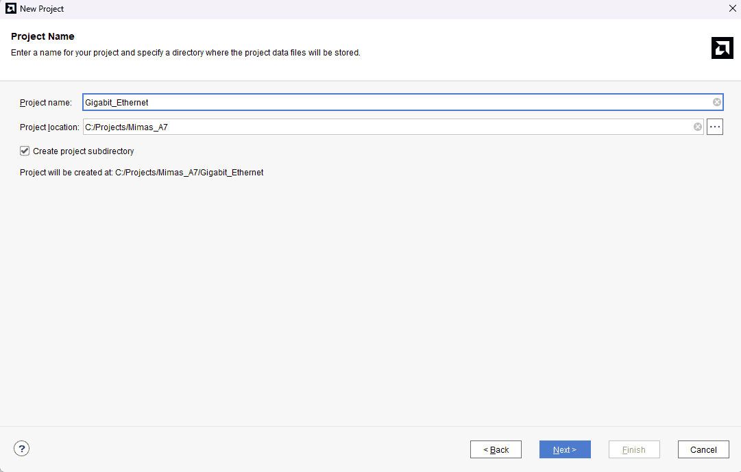
Enter a name for the project and save it at a suitable location. Check the option “Create project subdirectory”. Click Next to continue.
Step 3:
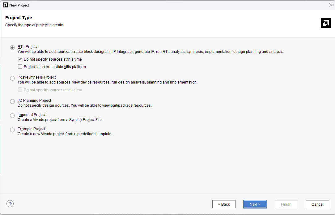
In the Project Type window, select RTL Project and check the “Do not specify sources at this time” option. Click Next.
Step 4:
In the Default Part window, select “Mimas_A7_50T” from the Boards option. Click Next to continue.
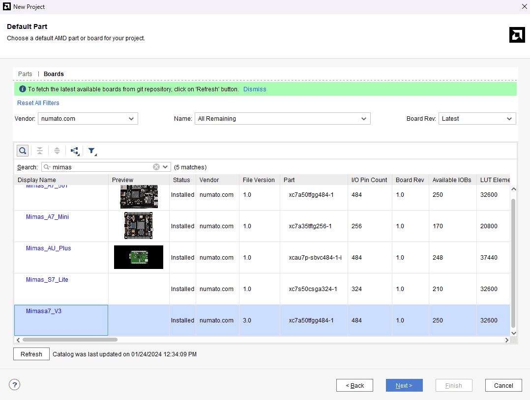
Click Finish to complete creating a new project. Vivado will create a new project with the selected settings.
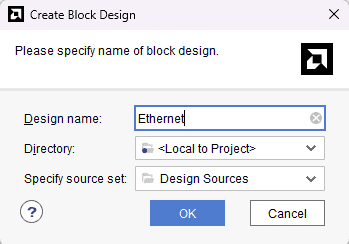
Step 5:
In the Flow Navigator panel, select Create Block Design under IP INTEGRATOR. Enter a name for the block design and click OK. An empty block design will be created
Step 6:
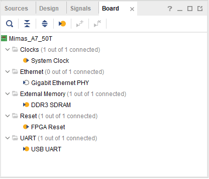
Click the Board tab. The default peripherals available for the Mimas A7 board will be displayed.
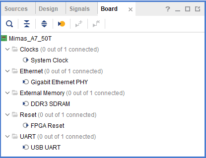
Drag and drop DDR3 SDRAM, USB UART, and System Clock into IPI Canvas.
Step 7:
Double click on Clocking Wizard IP block and change the settings as shown below. In the Output Clocks section, set:
- clk_out1 frequency to 100 MHz
- clk_out2 frequency to 200 MHz
- clk_out3 frequency to 125 MHz
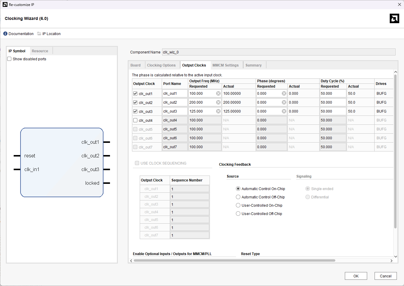
Click OK to customize the IP.
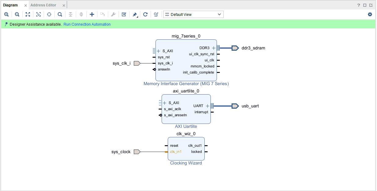
Ensure that sys_clk_i of Memory Interface Generator is connected to clk_out2.
Step 8:
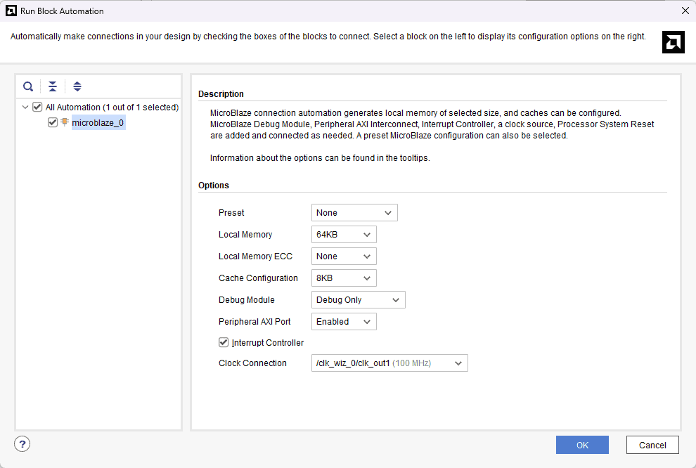
Click Add IP, search for MicroBlaze, and Add it.
Click Run Block Automation with 64 KB of local memory and interrupt controller enabled.
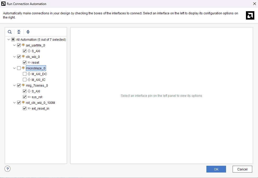
Click Run Connection Automation and select all to connect AXI interfaces of MIG, Uartlite IPs, and their clocks and resets. Uncheck the microblaze_0 part in it and click OK.
Step 9:
Drag & Drop Gigabit Ethernet PHY interface into IPI Canvas.
Note: Click on the “Report IP Status” section under the “Reports” tab to review the status of all IPs. If the status indicates “design linking” for the Ethernet IP, it is necessary to download and incorporate the corresponding hardware evaluation license (tri_mode_eth_mac@2015.4) to enable the proper functioning of the Ethernet IP.
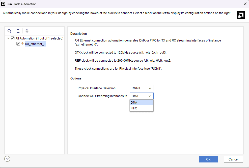
Step 10:
Run Block Automation for AXI Ethernet and select “DMA/FIFO” for the AXI Streaming interface.
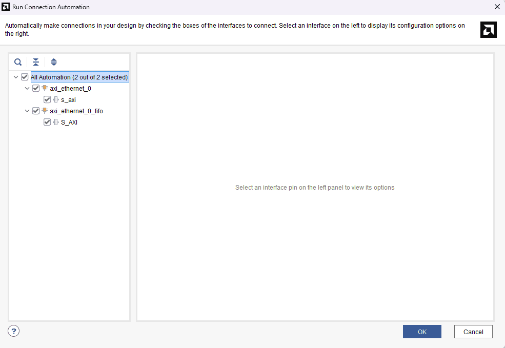
Step 11:
Click Run Connection Automation. Select the All Automation option and click OK.
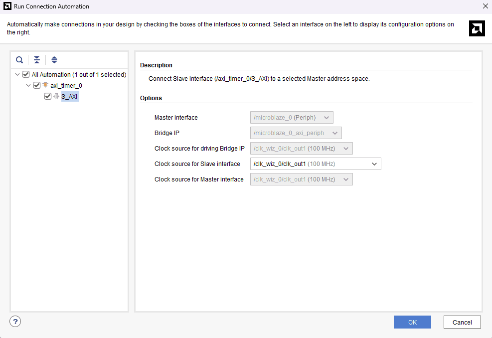
Step 12:
Add AXI Timer into IPI Canvas and click Run Connection Automation.
Step 13:
Customize the Concat IP block as shown below.
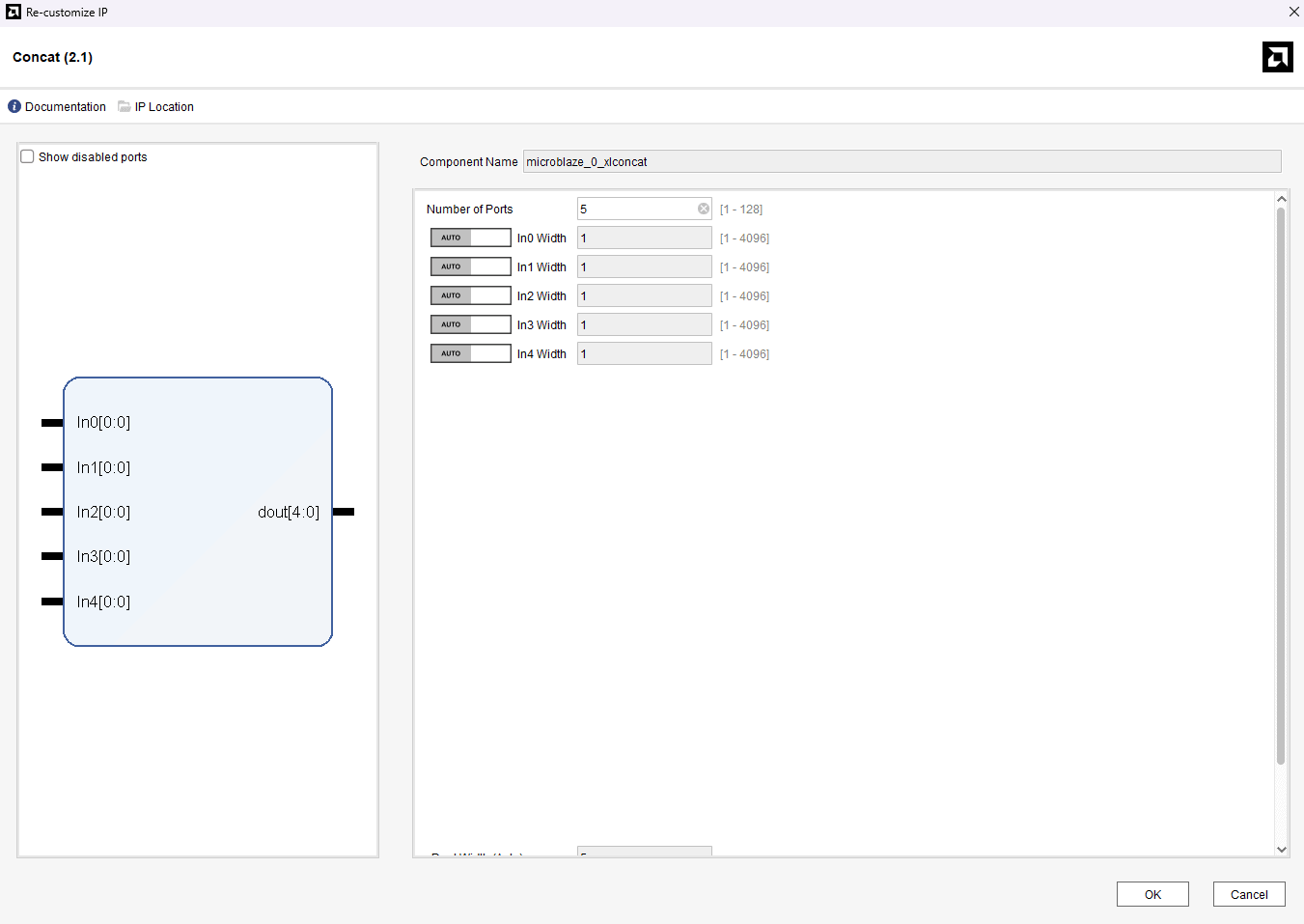
Route the following connections to the inputs of the Concat block:
- interrupt on AXI Uartlite block
- interrupt on AXI Timer block
- interrupt on AXI-Stream FIFO
- interrupt and mac_irq on AXI 1G/2.5G Ethernet Subsystem
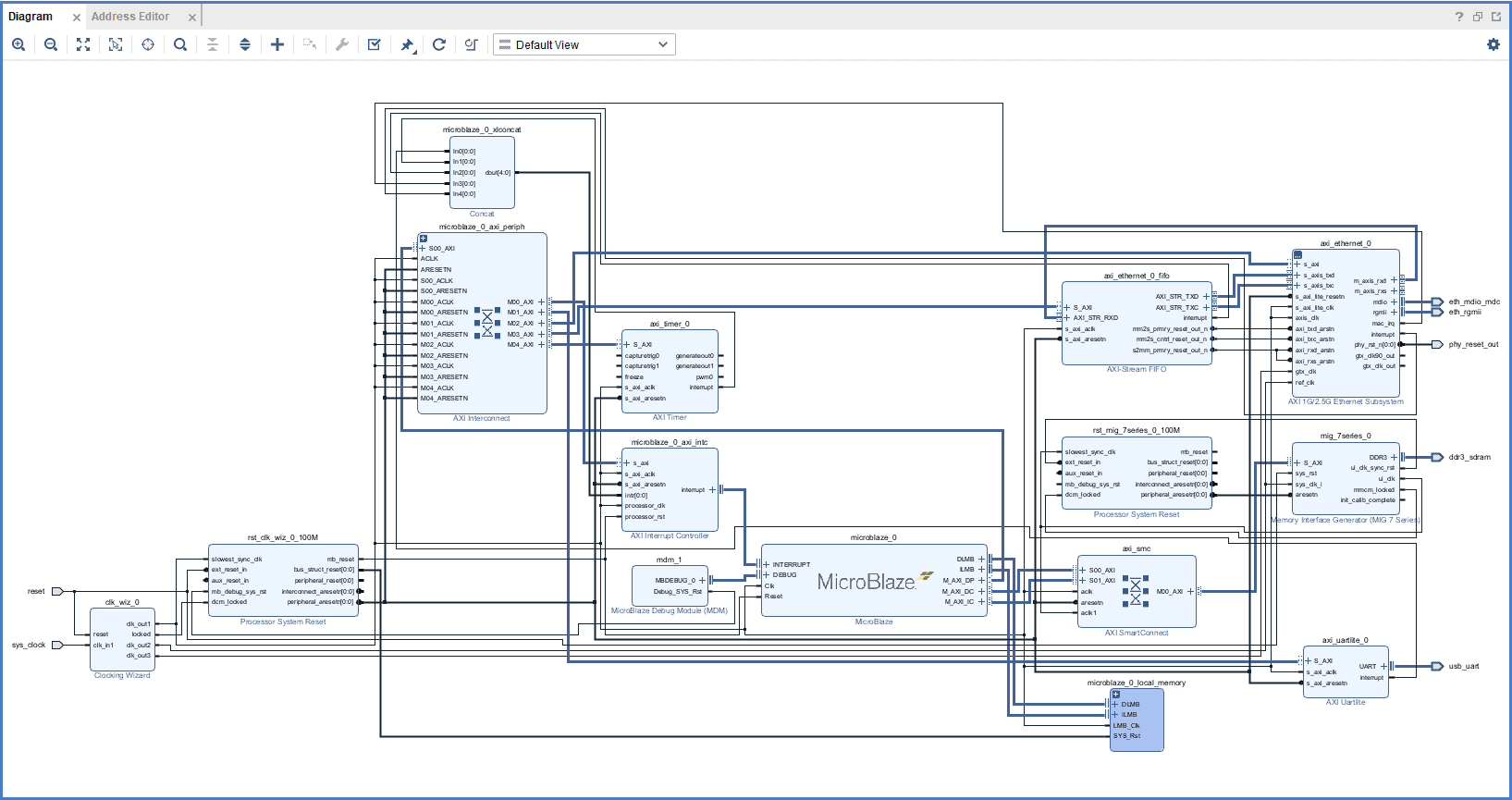
Make sure that the final design looks as shown above.
Step 14:
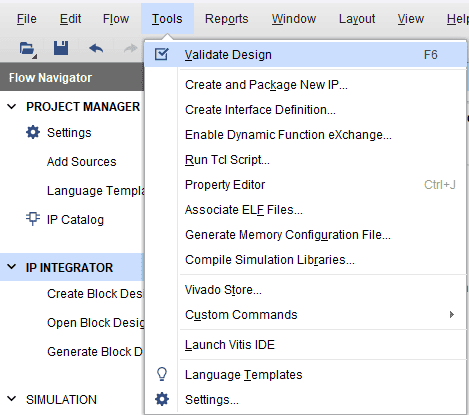
Select the Validate Design option from the Tools menu to ensure that connections are correct.
Step 15:
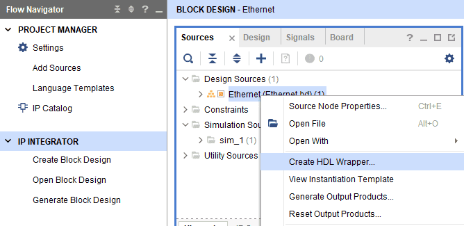
In the Sources window, right-click on the design and select Create HDL Wrapper. Click OK in the dialog box that appears.
Step 16:
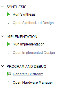
Click Generate Bitstream under the PROGRAM AND DEBUG section of Vivado to synthesize, implement and generate the bitstream.
Step 17:
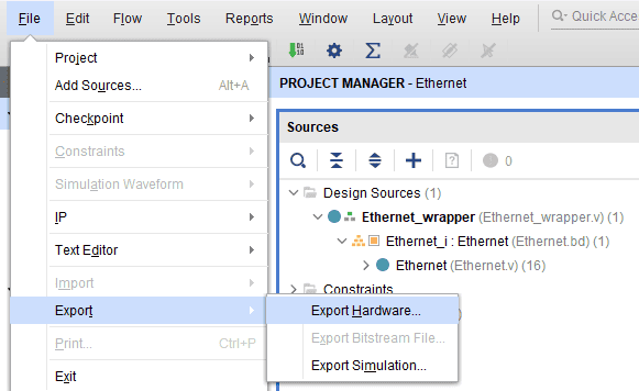
After generating the bitstream successfully, select Export -> Export Hardware from the File menu. Click Next.
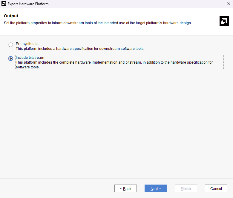
Select the “include bitstream” checkbox and click Next.
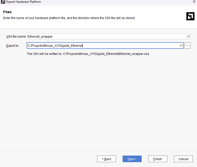
Provide the XSA file name and save it at a suitable location. Click Next and click Finish in the next dialog box.
Step 18:
Launch Vitis classic.
Note: In Vivado 2023.2, accessing Vitis via the tools menu inadvertently launches Vitis Unified instead of Vitis Classic, which is our preferred tool for project creation. To utilize Vitis Classic, it is necessary to launch it separately. This differentiation is applicable exclusively to versions released from 2023.2 onwards.
Step 19:
In Vitis, IDE window select Create Application Project and click Next in the dialog box that appears.
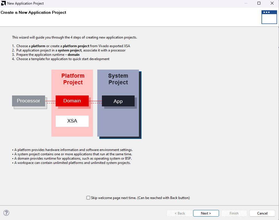
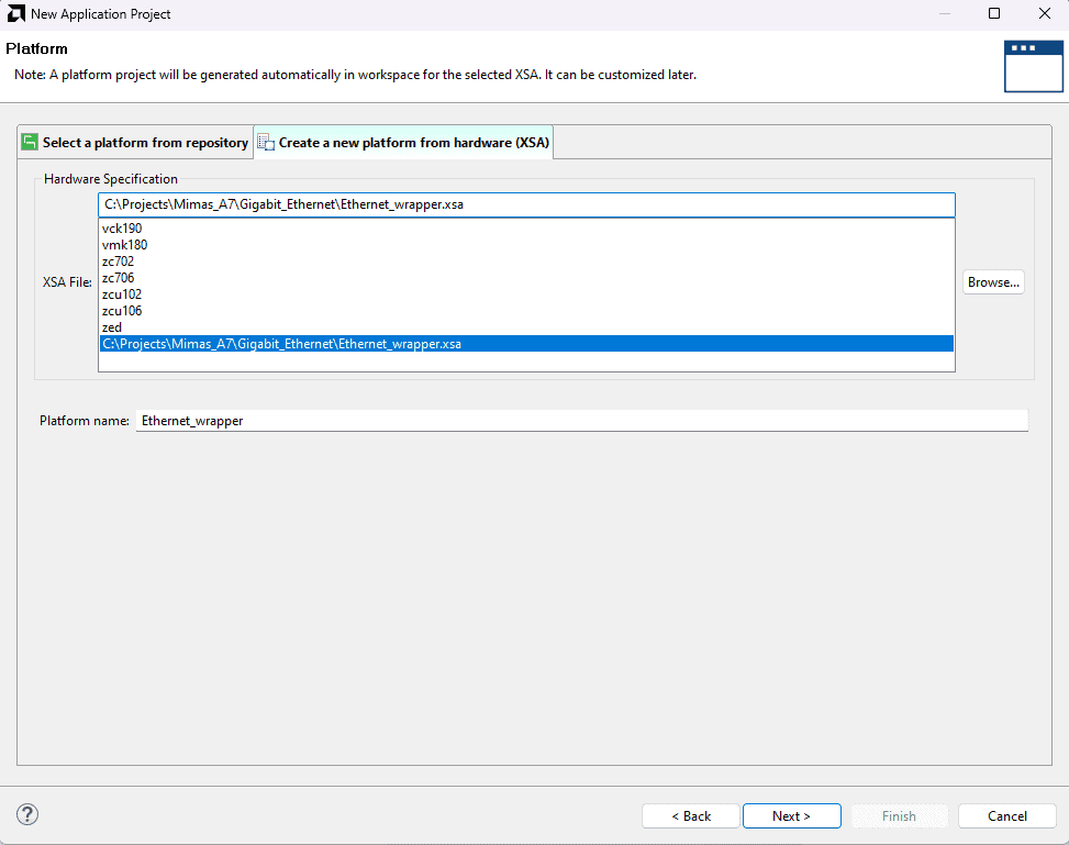
In the Platform, window select Create a new platform from the hardware Tab and import the XSA file which is already created (Provide XSA file location). Click Next.
In the Application Project Details window, give an appropriate name for the Vitis Project and click Next. Click Next in the Domain window.
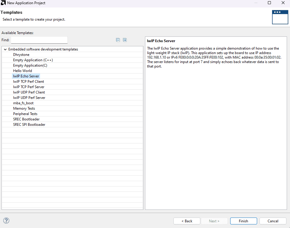
Select the lwIP Echo Server template from the list of available templates and click Finish.
Step 20:
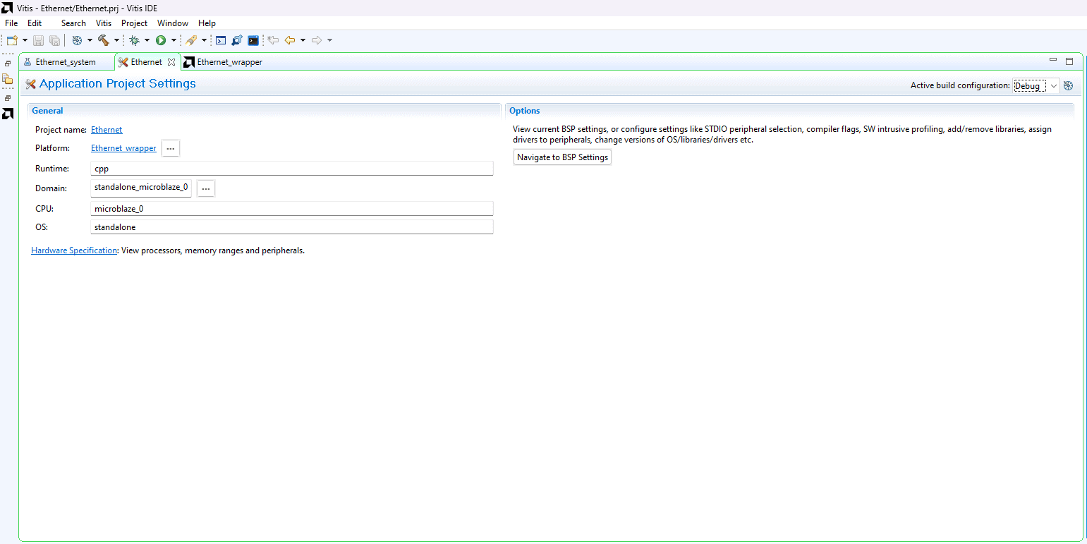
Select Navigate to BSP Settings from Application Project Settings.
Select Board Support Package and click on Modify BSP Settings option.
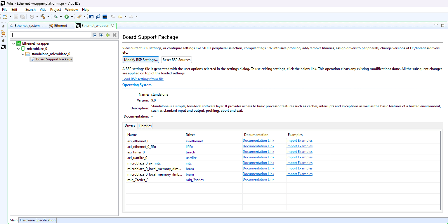
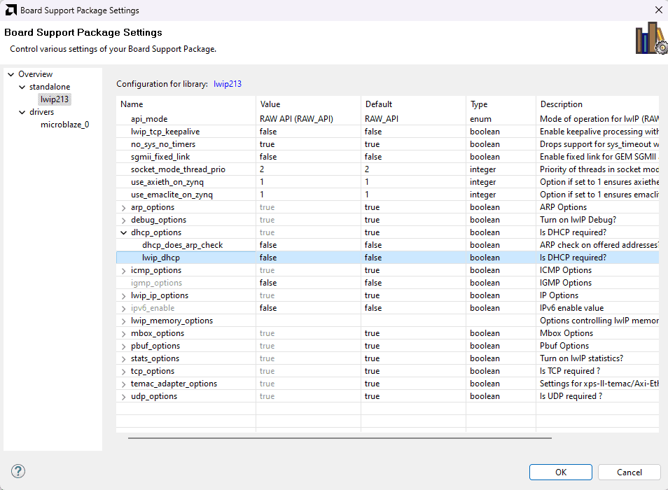
In the Board Support Package Settings window, select lwip (Iwip211) library, change the dhcp_options to “false” and ensure that “debug options” are “false”.
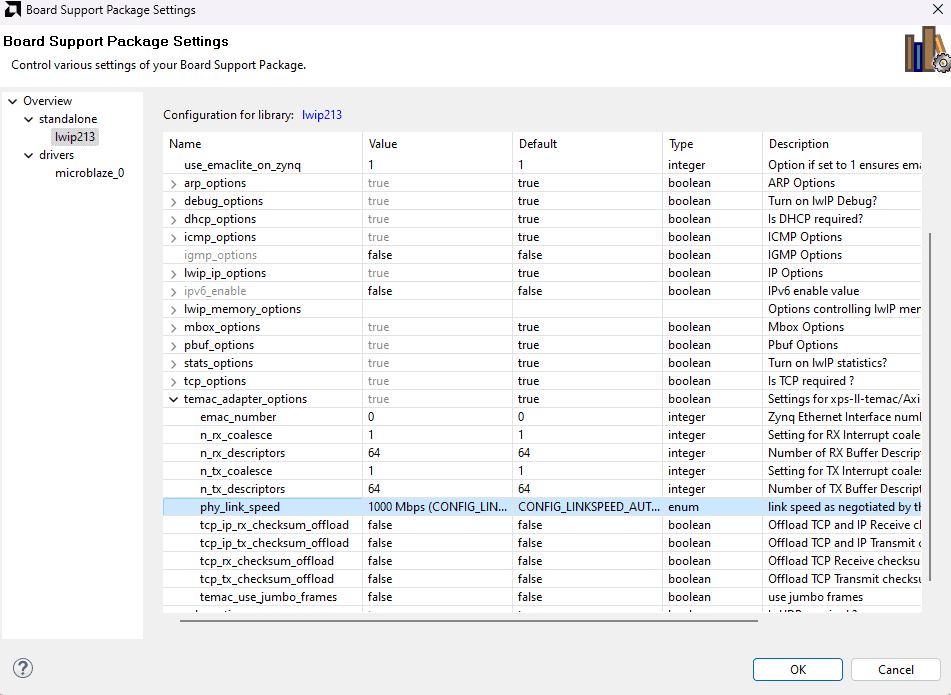
Select phy_link_speed in temac_adapter_options as CONFIG_LINKSPEED1000.
After changing the library settings, click OK. SDK will update the BSP automatically. If that didn’t happen for any reason, run a build manually.
Step 21:
Once the build is completed successfully, power up Mimas A7 FPGA Development Board using an external DC power supply and connect the Xilinx Platform USB cable to the board.
Step 22:
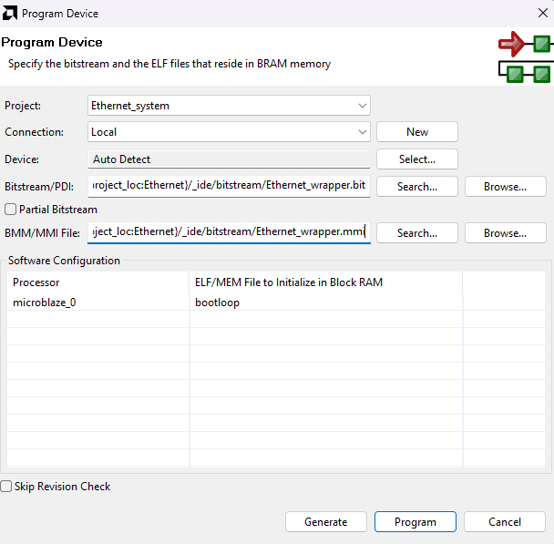
Program the FPGA on Mimas A7 with a simple boot loop program by selecting the Program FPGA option from the Xilinx menu.
Step 23:
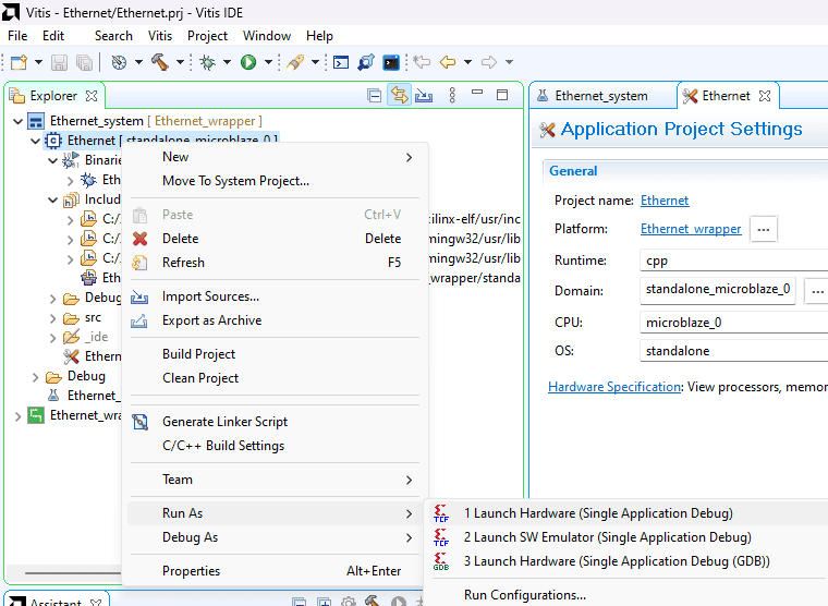
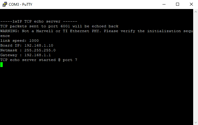
Open the COM port corresponding to Mimas A7 in any serial terminal (PuTTY, Tera Term, etc.) with a 115200 baud rate (if the UART IP baud rate is given 9600). Now, right-click on the .elf file in Project Explorer and select “Launch on Hardware” as shown below.
Observe the details displayed on the serial terminal.
Step 24:
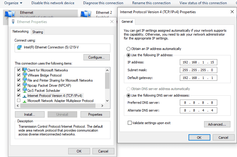
Connect the Ethernet cable to the board and the other end to the PC Ethernet port. Go to Control Panel. Go to Network and Internet -> Network and Sharing Centre -> Change adapter settings. Select “Change adapter settings”. Right-click on Ethernet, click properties, and select “IPv4”. Change the IPv4 address to 192.168.1.15 (any IP address can be used) and the default gateway to 192.168.1.1.
Step 25:
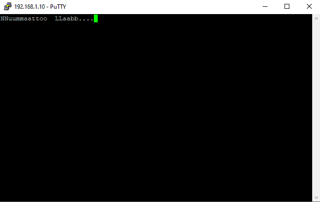
Open a telnet session with IP Address 192.168.1.10 (IP address as per main.c) at port 7, give input through the keyboard and observe the output. If you enter a character from the keyboard, you can observe the transmitted and echoed characters on telnet as shown.