Introduction:
The FTDI FT2232H USB 2.0 chip available on-board Styx provides users with a FIFO interface for data transfer between FPGA and host PC. The FT2232H chip features two channels or ports, which can be configured into various modes like UART, FIFO, JTAG, etc. On Styx, channel B is used for FPGA configuration and flash programming whereas Channel A is available for custom usage. This article demonstrates communication between the host and the board using Synchronous FIFO mode via channel A of FT2232H. The Channel A of FT2232H, when configured as FIFO, acts as a USB-FIFO bridge between host and FPGA. Synchronization is done using the 60 MHz clock available on FT2232H. Let’s get started!
Prerequisites:
- Hardware:
- Styx Xilinx Zynq FPGA Module
- Xilinx Platform Cable USB II (optional)
- Software:
- Vivado 2017.3 or later
- Python 2.7
Step 1:
Download and install Vivado Board Support Package files for your Styx from here. Follow the README.md file on how to install Vivado Board Support Package files for Numato Lab boards.
Step 2:
Open Vivado and select ‘Create Project’

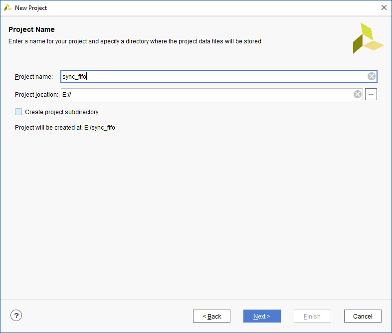
Step 3:
Click ‘Next’, In Project Name tab, give appropriate project name and select the directory where you want to save the project.
Step 4:
Click Next without making any changes until you see the ‘Default Part’ tab and select your ‘Styx’ from the ‘Boards’ option. If it is not listed, make sure board support files are installed correctly.

Step 5:
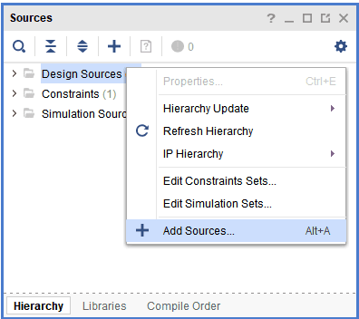
Right-Click ‘Design Sources’ select ‘Add Sources’. It will open a configuration window for adding Verilog file.
Step 6:
Download and extract the RTL Code files from here. Now Click ‘Add Files’, select all files and add them to the project.
Here, FTDI’s Synchronous FIFO interface is used to perform data transfer between FPGA and host PC. As the operation is Synchronous, the data transfers occur in synchronization with clock. The speed is much higher than that of asynchronous FIFO. To use the synchronous FIFO transfer mode available on FT2232H, its hardware and driver must be configured as 245 FIFO and D2XX respectively. In this article, Channel A of FT2232H is configured as FIFO, which provides the following signals:
data: It is a bi-directional bus carrying the 8-bit FIFO data.
rxf_n: It is an active low signal. When de-asserted, does not read data from FIFO. When it is enabled, it indicates that there is some data available in FIFO, the data is read after asserting rd_n.
txe_n: It is an active low signal. When de-asserted, does not write data to FIFO. When it is asserted, data can be written to FIFO if wr_n is asserted.
rd_n: It is an active low signal. When asserted, data is driven onto data bus from FIFO.
wr_n: It is an active low signal. When asserted, data written on data bus is driven into FIFO.
oe_n: it is an active low output enable input signal. When asserted, data is driven ondata bus, then rd_n is enable after 1 clock period.
In the RTL code, FSM is implemented, it checks whether there is some data in FIFO for reading (indicated by pending_read), if so, oe_n is asserted, followed by an assertion of rd_n, data is read. After this, oe_n and rd_n signals are de-asserted. If there is data to be written (indicated by pending_write), wr_n is enabled and data is written into FPGA.

Step 7:
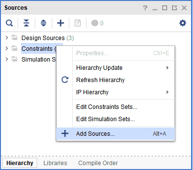
Right-Click Constraints and select ‘Add sources’.
Step 8:
Click Next and then ‘Create File’. Give a File name and Click Finish.
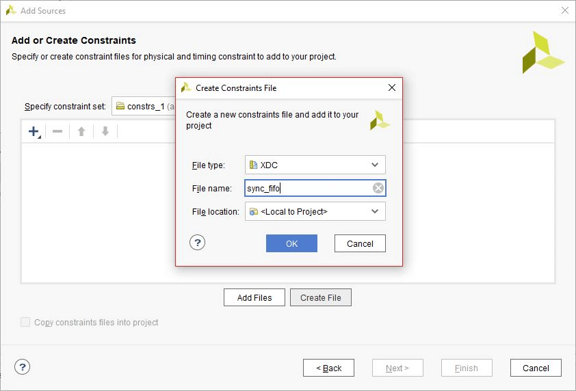
Step 9:
Copy the following constraints in .xdc file.
set_property IOSTANDARD LVCMOS33 [get_ports clk]
set_property PACKAGE_PIN Y6 [get_ports clk]
set_property IOSTANDARD LVCMOS33 [get_ports rst]
set_property PACKAGE_PIN H18 [get_ports rst]
set_property PULLUP true [get_ports rst]

set_property IOSTANDARD LVCMOS33 [get_ports {data[7]}]
set_property IOSTANDARD LVCMOS33 [get_ports {data[6]}]
set_property IOSTANDARD LVCMOS33 [get_ports {data[5]}]
set_property IOSTANDARD LVCMOS33 [get_ports {data[4]}]
set_property IOSTANDARD LVCMOS33 [get_ports {data[3]}]
set_property IOSTANDARD LVCMOS33 [get_ports {data[2]}]
set_property IOSTANDARD LVCMOS33 [get_ports {data[1]}]
set_property IOSTANDARD LVCMOS33 [get_ports {data[0]}]

set_property PACKAGE_PIN AB22 [get_ports {data[7]}]
set_property PACKAGE_PIN AA22 [get_ports {data[6]}]
set_property PACKAGE_PIN W22 [get_ports {data[5]}]
set_property PACKAGE_PIN V22 [get_ports {data[4]}]
set_property PACKAGE_PIN U21 [get_ports {data[3]}]
set_property PACKAGE_PIN U22 [get_ports {data[2]}]
set_property PACKAGE_PIN T21 [get_ports {data[1]}]
set_property PACKAGE_PIN T22 [get_ports {data[0]}]

set_property IOSTANDARD LVCMOS33 [get_ports txe_n]
set_property PACKAGE_PIN Y21 [get_ports txe_n]

set_property IOSTANDARD LVCMOS33 [get_ports rxf_n]
set_property PACKAGE_PIN W20 [get_ports rxf_n]

set_property IOSTANDARD LVCMOS33 [get_ports wr_n]
set_property PACKAGE_PIN W21 [get_ports wr_n]

set_property IOSTANDARD LVCMOS33 [get_ports rd_n]
set_property PACKAGE_PIN Y20 [get_ports rd_n]

set_property IOSTANDARD LVCMOS33 [get_ports oe_n]
set_property PACKAGE_PIN U20 [get_ports oe_n]

set_property IOSTANDARD LVCMOS33 [get_ports siwu]
set_property PACKAGE_PIN V20 [get_ports siwu]

set_property IOSTANDARD LVCMOS33 [get_ports clkout]
set_property PACKAGE_PIN L18 [get_ports clkout]
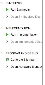
Step 10:
In Project Manager Tab, Click ‘Run Synthesis’. If Synthesis is successful, Click ‘Run Implementation’ and on successful implementation select ‘Generate Bitstream’.
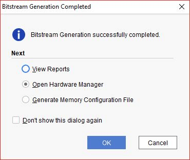
Step 11:
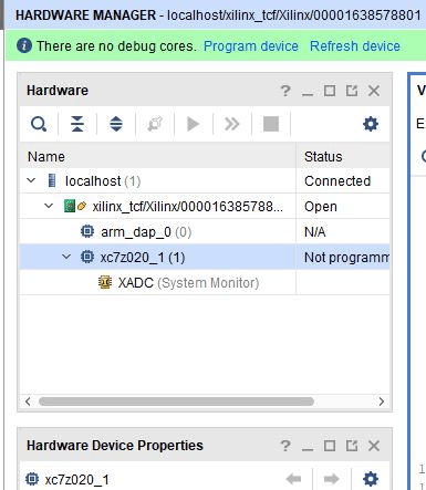
After the successful generation of the bitstream, Open Hardware Manager.
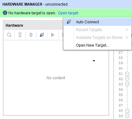
Step 12:
Click ‘Open target’ and ‘Auto Connect’. It will connect to the Module. Make sure you have connected the board to JTAG, Power supply, and USB.
Step 13:
Click ‘Program Device’. It will pop up a new window. Program the bit file by Clicking ‘Program’.
Step 14:
Once the device is programmed, program proper FTDI Settings for FIFO to work.
Change FTProg settings as follows. Go to Device:0 -> Hardware Specific -> Port A -> Hardware and select RS245 FIFO. Now go to Hardware Specific -> Port A -> Driver and select D2XX.
Step 15:
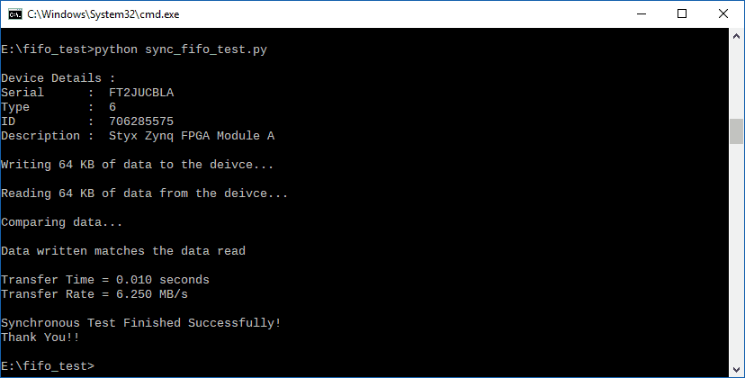
Now, To check if Asynchronous FIFO is working as expected, write some data through FIFO, read it back and compare it. If the data written matches the data that is read then it is successfully implemented.
To check this, copy the following python code in a text editor and save it as ‘sync_fifo_test.py’
from __future__ import print_function
import time
import random

import ftd2xx

BLOCK_LEN = 2048 * 32

def init():
 dev = ftd2xx.openEx('Styx Zynq FPGA Module A',2)
 time.sleep(0.1)
 dev.setTimeouts(5000, 5000)
 time.sleep(0.1)
 dev.setBitMode(0xff, 0x00)
 time.sleep(0.1)
 dev.setBitMode(0xff, 0x40)
 time.sleep(0.1)
 dev.setUSBParameters(0x10000, 0x10000)
 time.sleep(0.1)
 dev.setLatencyTimer(2)
 time.sleep(0.1)
 dev.setFlowControl(ftd2xx.defines.FLOW_RTS_CTS, 0, 0)
 time.sleep(0.1)
 dev.purge(ftd2xx.defines.PURGE_RX)
 time.sleep(0.1)
 dev.purge(ftd2xx.defines.PURGE_TX)
 time.sleep(0.1)
 return dev

tx_data = str(bytearray([ random.randrange(0, 256) for i in range(BLOCK_LEN)]))

dev = init()
print("\nDevice Details :")
print("Serial : " , dev.getDeviceInfo()['serial'])
print("Type : " , dev.getDeviceInfo()['type'])
print("ID : " , dev.getDeviceInfo()['id'])
print("Description : " , dev.getDeviceInfo()['description'])
print("\nWriting %d KB of data to the deivce..." % (BLOCK_LEN / 1024))
ts = time.time()
written = dev.write(tx_data)
print("\nReading %d KB of data from the deivce..." % (BLOCK_LEN / 1024))
rx_data = dev.read(BLOCK_LEN)
te = time.time()

p = te - ts
print("\nComparing data...\n")
if (tx_data == rx_data):
 print("Data written matches the data read\n")
else:
 print("Data verification failed\n")

dev.close()
print("Transfer Time = %.3f seconds" % p)
speed = (BLOCK_LEN / 1024./1024 / p)
print("Transfer Rate = %.3f MB/s" % speed)

print("\nSynchronous Test Finished Successfully!\nThank You!!")
Open command prompt in the file directory and give the following command
python sync_fifo_test.py