Introduction
HDMI (High Definition Multimedia Interface) is used to transfer digital audio and video data between devices with high-quality and high-bandwidth. The pixel data is serially transferred at ten times of pixel clock frequency using TMDS (Transition Minimized Differential Signalling) to minimize the transitions between 1s and 0s. This article actually demonstrates DVI-D (subset of HDMI) output using Galatea PCI Express Spartan 6 FPGA Development Board. Both DVI-D and HDMI uses the same video format standard. So, all HDMI monitors should be capable of receiving the DVI-D signals transported over HDMI cable. The Galatea IP4776CZ38 HDMI Expansion Module features dual HDMI buffered output ports. This article demonstrates generating dual, independent HDMI output from the Galatea PCI Express Spartan 6 FPGA Development Board.
Prerequisites
- Hardware:
- Galatea PCI Express Spartan6 FPGA Development Board
- Galatea IP4776CZ38 HDMI Expansion Module
- Xilinx Platform Cable USB II JTAG
- HDMI monitors: x2
- HDMI Cables: x2
- Galatea 12V ATX Power Supply
- Software:
- Xilinx ISE Design Suite 14.7
Let’s get started
The following steps will walk you through the process of creating the dual-HDMI output project using Xilinx ISE Design Suite.
Step 1:
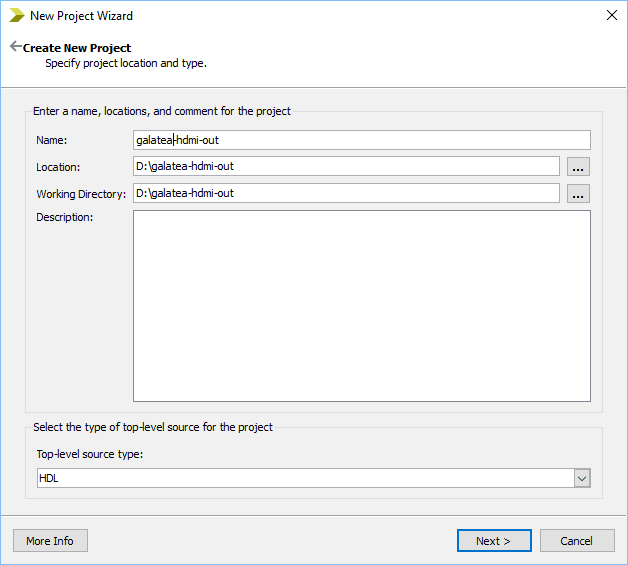
Open Xilinx ISE Design Suite and select “New Project” from “File” menu. The “New Project Wizard” configuration window will open. Select a convenient project location and enter a name for the project. In this article, the author is used “galatea-hdmi-out” as the project name. Click “Next” to proceed.
Step 2:
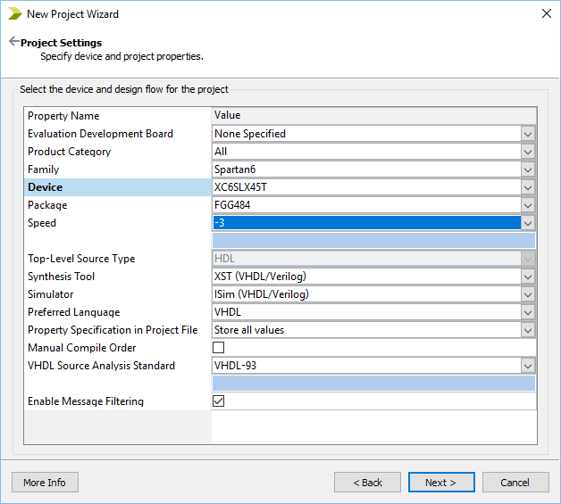
Specify the device and project settings (Family: Spartan 6, Device: XC6SLX45T, Package: FGG484 and Speed: -3) in the “Project Settings” tab as shown below. Click “Next” and “Finish” to create a new ISE project with the selected settings.
Step 3:
Download and extract the RTL source files from here. Under “Design” tab, right click and click “Add Source…” to add the RTL source files from the extracted folder.
The HDMI interface has three pairs of differential data signals (One pair for each color i.e Red, Green and Blue) and one pair of differential clock signals. The signals are:
data_p[2:0] & data_n[2:0]: These are HDMI/DVI-D differential signals carrying the video data to be displayed on the screen.clk_p & clk_n: HDMI pixel clock differential pair of signals.
First, VGA signals are generated inside vga module. Then the VGA signals are encoded to 10-bits per channel and the data is then serialized to 10x of pixel clock rate. Finally, the three channels along with pixel clock are driven out using TMDS differential drivers.
In the top module (topmodule), the main dvid generation module (dvid_test) is instantiated twice to generate two HDMI streams for the dual-HDMI outputs available on Galatea HDMI expansion module. The clock generation module (clocking) also instantiated along with dvid generation module to generate the required clocks for VGA and DVI-D. The submodules clocking and dvid_test are explained below.
clocking: This module is used to generate the required clocks for VGA and DVI-D. It takes 100MHz system clock from the onboard oscillator of Galatea as input and derives other DVI-D and VGA clocks from it. The project uses the following clocks
- CLK_IN = 100MHz: The clocking module run on this clock.
- CLK_DVI = 125MHz: This clock is 5 times of pixel clock frequency and its frequency for 640×480@60Hz resolution is 125MHz. This clock is generated along with its inverted version (180 degrees out of phase) to serialize the pixel data at 10 times of its pixel clock frequency.
- CLK_DVIn= 125MHz: This clock is an inverted version of
CLK_DVIand is used to serialize the pixel data at 10 times of its pixel clock frequency. - CLK_VGA = 25MHz : This is a primary pixel clock frequency based on the resolution. In this article, 640×480@60Hz resolution is used so, the pixel clock frequency is 25MHz.
dvid_test: In this submodule, dvid and vga submodules are instantiated. Each of the submodules are explained below.
vga: VGA signals are generated with 640×480@60Hz resolution at 25 MHz pixel clock frequency.
dvid: Clock signals generated from the clocking module and the VGA signals from vga module are given as input to this module and the DVI-D TMDS signals are generated as the output. It uses TMDS_encoder module to generate TMDS signals. TMDS uses 8b/10b encoding in which the 8-bit color data (red, green & blue) generated in VGA module and is converted to 10 bits. Then this data is serialized using ODDR2 (Double Data Rate primitive). The 10-bit TMDS data is generated at 25 MHz. ODDR2 uses 5 times the frequency of pixel clock (i.e. 125MHz) to serialize the 10-bit encoded data. Note that ODDR2 serializes 2-bits in 1 clock cycle of 125MHz clock. This serialized data is converted into differential signals in the top module (dvid_test) using OBUFDS drivers.
Step 4:
Create a constraint file and copy paste the following constraints.
CONFIG VCCAUX = "3.3" ;
# Clock 100 MHz
NET "clk_in" LOC = "G9" | IOSTANDARD = LVCMOS33 | Period = 100 MHz;
NET "reset"               IOSTANDARD = LVCMOS33 | DRIVE = 8 | SLEW = FAST | PULLDOWN;
#
# hdmi 0
#
NET "data0_p[0]" LOC = "C5"  | IOSTANDARD = "TMDS_33" | DRIVE = 8 | SLEW = FAST ;
NET "data0_n[0]" LOC = "A5"  | IOSTANDARD = "TMDS_33" | DRIVE = 8 | SLEW = FAST ;
NET "data0_p[1]" LOC = "G8"  | IOSTANDARD = "TMDS_33" | DRIVE = 8 | SLEW = FAST ;
NET "data0_n[1]" LOC = "F9"  | IOSTANDARD = "TMDS_33" | DRIVE = 8 | SLEW = FAST ;
NET "data0_p[2]" LOC = "H10" | IOSTANDARD = "TMDS_33" | DRIVE = 8 | SLEW = FAST ;
NET "data0_n[2]" LOC = "H11" | IOSTANDARD = "TMDS_33" | DRIVE = 8 | SLEW = FAST ;
NET "clk0_p"     LOC = "H12" | IOSTANDARD = "TMDS_33" | DRIVE = 8 | SLEW = FAST ;
NET "clk0_n"     LOC = "G11" | IOSTANDARD = "TMDS_33" | DRIVE = 8 | SLEW = FAST ;

#
# hdmi 1
#
NET "data1_p[0]" LOC = "C17" | IOSTANDARD = "TMDS_33" | DRIVE = 8 | SLEW = FAST ;
NET "data1_n[0]" LOC = "A17" | IOSTANDARD = "TMDS_33" | DRIVE = 8 | SLEW = FAST ;
NET "data1_p[1]" LOC = "G16" | IOSTANDARD = "TMDS_33" | DRIVE = 8 | SLEW = FAST ;
NET "data1_n[1]" LOC = "F17" | IOSTANDARD = "TMDS_33" | DRIVE = 8 | SLEW = FAST ;
NET "data1_p[2]" LOC = "D18" | IOSTANDARD = "TMDS_33" | DRIVE = 8 | SLEW = FAST ;
NET "data1_n[2]" LOC = "D19" | IOSTANDARD = "TMDS_33" | DRIVE = 8 | SLEW = FAST ;
NET "clk1_p"     LOC = "E16" | IOSTANDARD = "TMDS_33" | DRIVE = 8 | SLEW = FAST ;
NET "clk1_n"     LOC = "F16" | IOSTANDARD = "TMDS_33" | DRIVE = 8 | SLEW = FAST ;
Step 5:
Go to “Design” tab and double-click “Generate Programming File” to generate the bitstream.
Step 6:
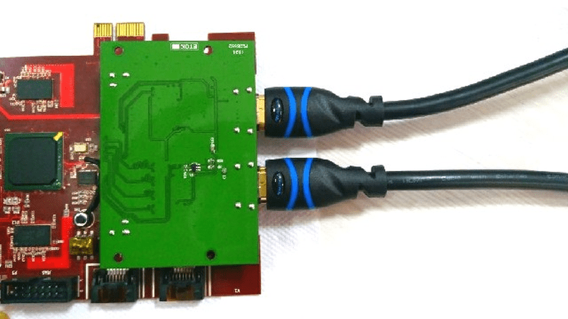
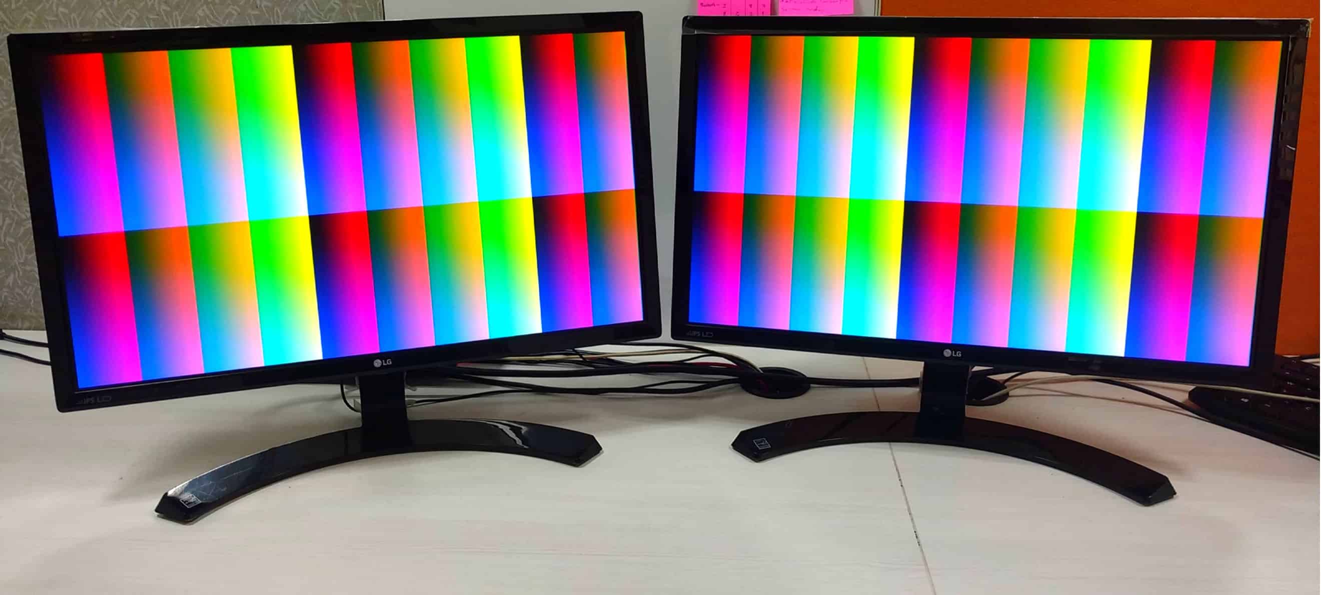
Once the bitstream is generated successfully, connect the Galatea IP4776CZ38 HDMI expansion module to header P4 of Galatea PCI Express Spartan 6 FPGA Development Board and connect two HDMI cables from HDMI expansion module to the two HDMI-capable monitors. Power up the Galatea board and program the generated bit file. Once the bitstream is programmed, both the monitors should display a color pattern at 640×480@60Hz resolution as shown below.
That’s it! Congratulations if you got the design working. There are a number of avenues for improvement and experimenting such as trying resolutions, patterns, framebuffer etc. You are encouraged to go ahead and try those.