Introduction
The purpose of this article is to help readers understand how to use DDR3 memory available on Callisto K7 using Xilinx MIG 7 IP core easily. The MIG 7 IP core provides users with two interface options: User Interface (a wrapper over Native interface) and the AXI4 Interface. This article will demonstrate how to test the DDR3 memory on Callisto K7 using Memory tests template.
Prerequisites:
Hardware:
- Callisto Kintex 7 USB 3.1 FPGA Module
- Xilinx Platform Cable USB II JTAG debugger.
- USB A to USB Type C cable
Software:
- Vivado Design Suite with Vitis installed (Version 2023.2.1).
Creating Microblaze based Hardware Platform for Callisto K7
The following steps will walk you through the process of creating a new project with Vivado and building a hardware platform with a Microblaze soft processor using the Vivado IP integrator. This article uses the Callisto K7 USB 3.1 FPGA Module but any compatible FPGA platform can be used with minor changes to the steps. Screenshots are added wherever possible to make the process easier for the reader.
Step 1:
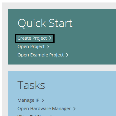
Open Vivado and select “Create Project” from the “Quick Start” section.
Step 2:
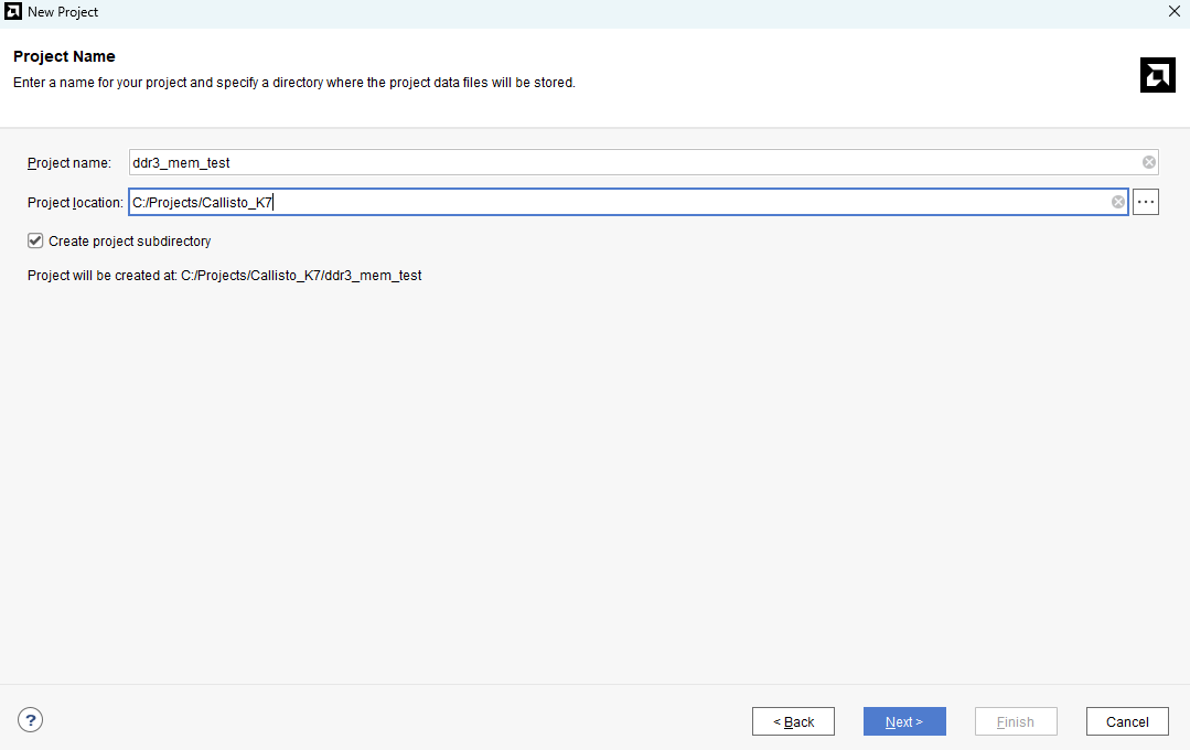
Click “Next” and enter a name for the project in the “Project Name” section. Click “Next” till you reach the “Default Part” page.
Step 3:
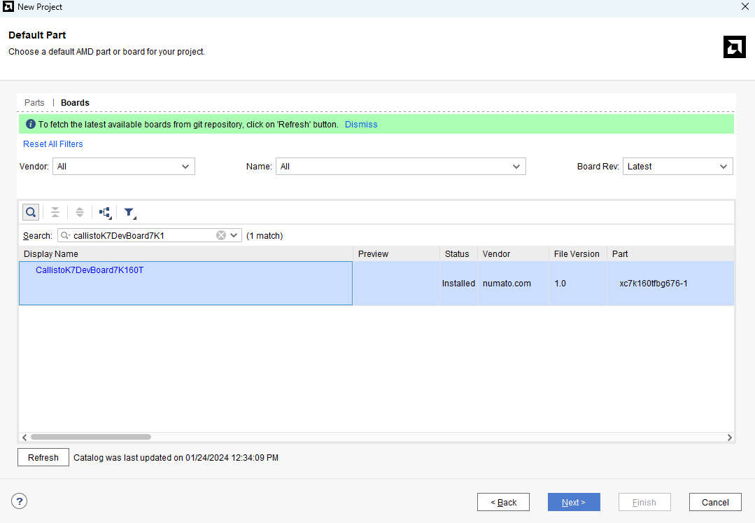
Select the “Boards” tab in the “Default Part” page and choose “numato.com” as Vendor. Select “CallistoK7DevBoard7K160T” from the boards’ list and click “Next”. If the Callisto K7 is not listed, make sure the board support files are installed correctly.
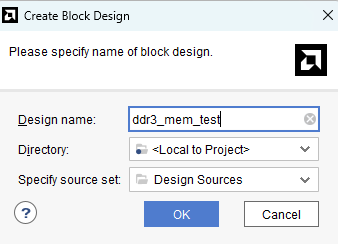
Step 4:
Click “Next” and then “Finish” to create the project. Click “Create Block Diagram” from the IP integrator section on left in the Xilinx Vivado window, enter a name for block design and click OK.
Step 5:
Select “Board” in the “Block Design” block. The default peripherals available for the Callisto K7 Board will be listed as shown in the image below.
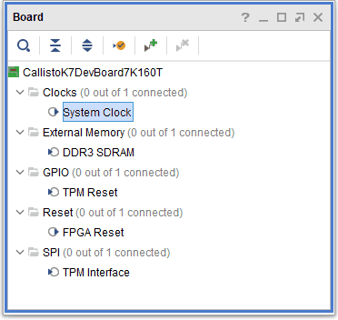
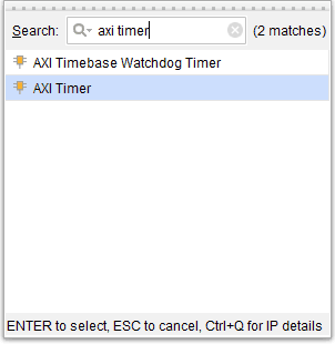
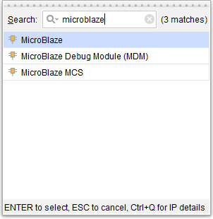
Step 6:
Add the System Clock and the DDR3 SDRAM peripherals to the design by double-clicking on the corresponding peripherals. In the design window, right-click and select “Add IP” from the popup menu. Search for “Microblaze” and “AXI timer” and add them to the design by double-clicking on them.
Step 7:
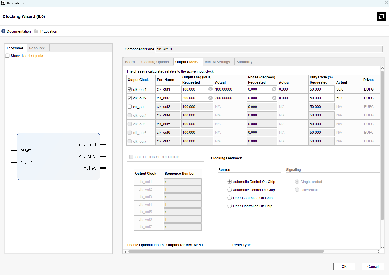
Double-click on the Clock IP block and configure it as shown below.
Step 8
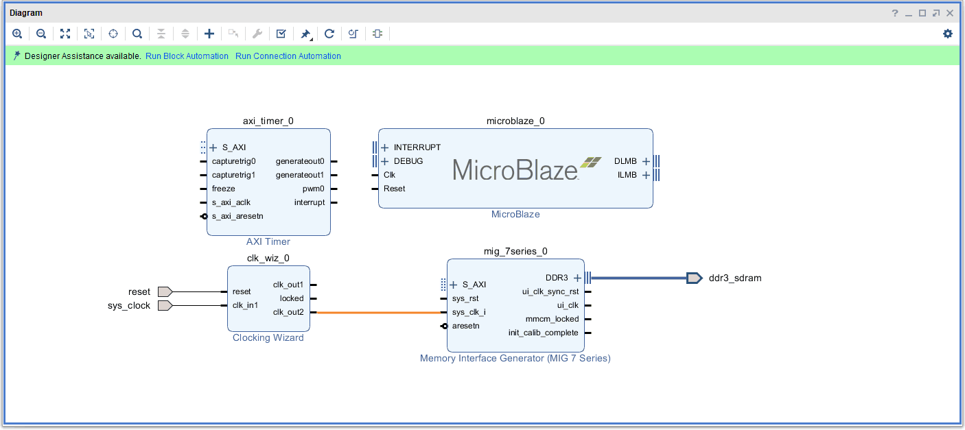
Remove the existing connection to “sys_clk_i” and connect “clk_out2” from the clocking Wizard to the “sys_clk_i” port of the “MIG 7 Series” block as shown in the image below.
Step 9:
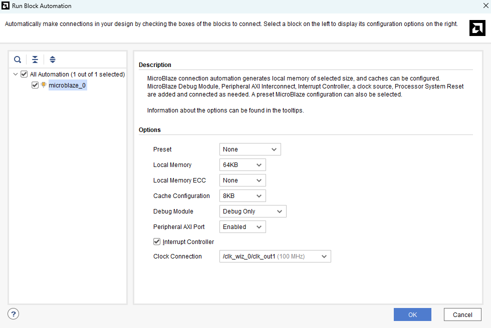
Click “Run Block Automation” in the top left corner of the window to complete the design. Select the settings as shown in the below image. Click “OK” for Vivado to automatically configure the blocks for you. Once Block Automation is complete, “Run Connection Automation” so Vivado can connect the blocks together to make a complete system.
Step 10:
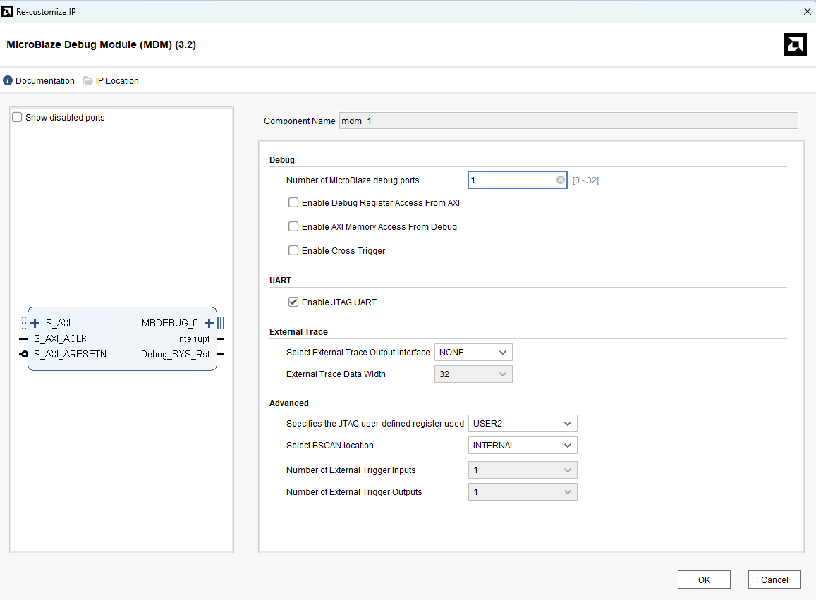
Double-click on the MicroBlaze Debug Module (MDM) IP block and select the “Enable JTAG UART” option as shown in the image below.
Next, connect the interrupt output from AXI Timer and MicroBlaze Debug Module to the Concat block as shown in the picture below. The relevant blocks are highlighted in red and the connections are highlighted in orange.
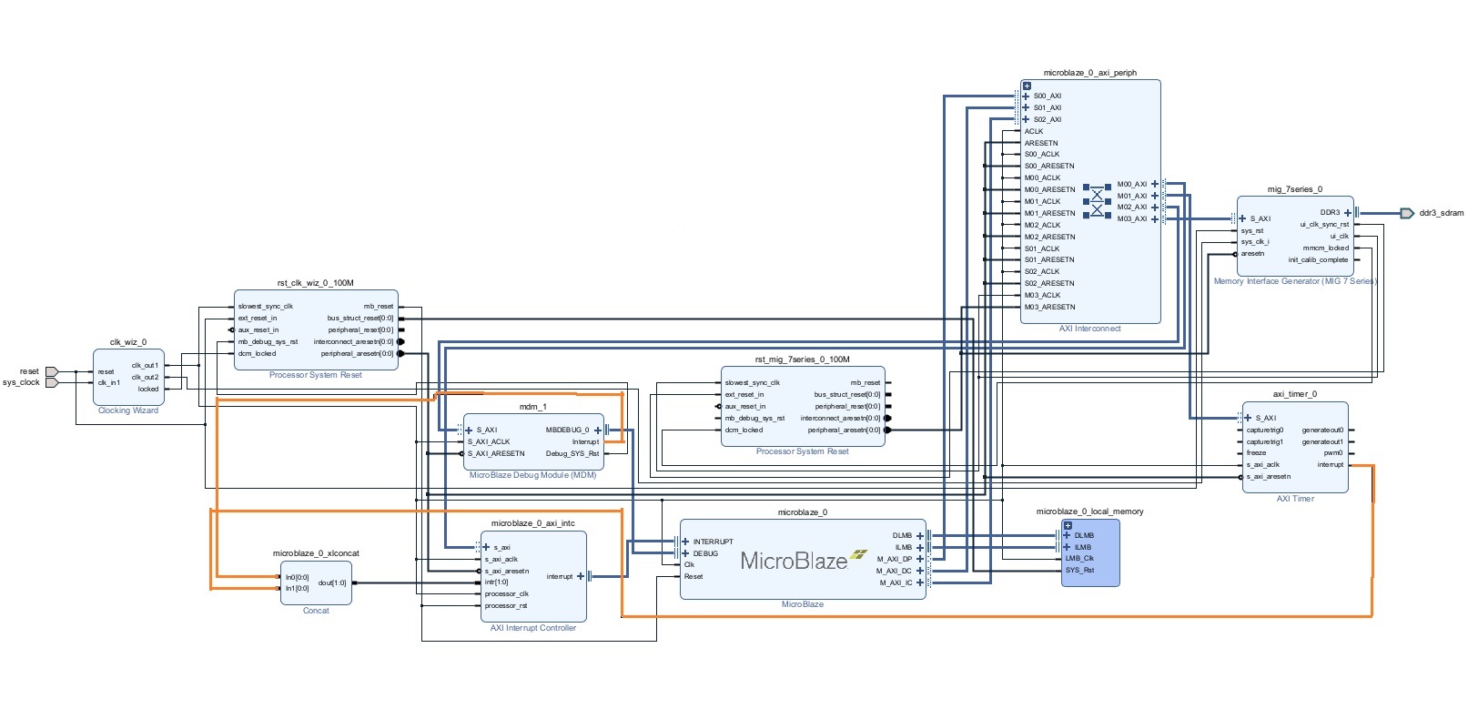
Run connection automation once again for Vivado to complete the remaining connections.
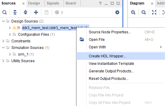
Step 11:
Save the design and then right-click on the block design file (.bd extension) in the “Sources” window, and select “Create HDL Wrapper” from the popup menu. Click “OK” on the window that appears to finish generating the wrapper.
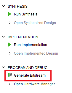
Step 12:
Click “Generate Bitstream” under the “PROGRAM AND DEBUG” section of Vivado to synthesize, implement and generate the bitstream.
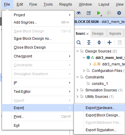
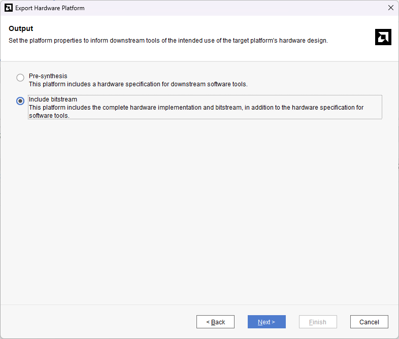
Step 13:
After the implementation and generation of the bitstream are successfully completed, we need to export the hardware along with bitstream. Go to the “File” menu, and select “Export -> Export Hardware”. Select “Include bitstream” and click “OK”.
Step 14:
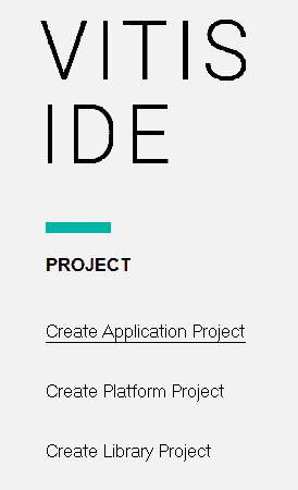
Launch Vitis IDE. In the Vitis window, select “Create Application Project” and click “Next” in the dialog box that appears.
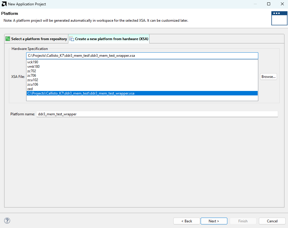
In the “Platform” window, select “Create a new platform from hardware” tab and import the “XSA file” which is already created (Provide XSA file location). Click “Next“.
Step 15:
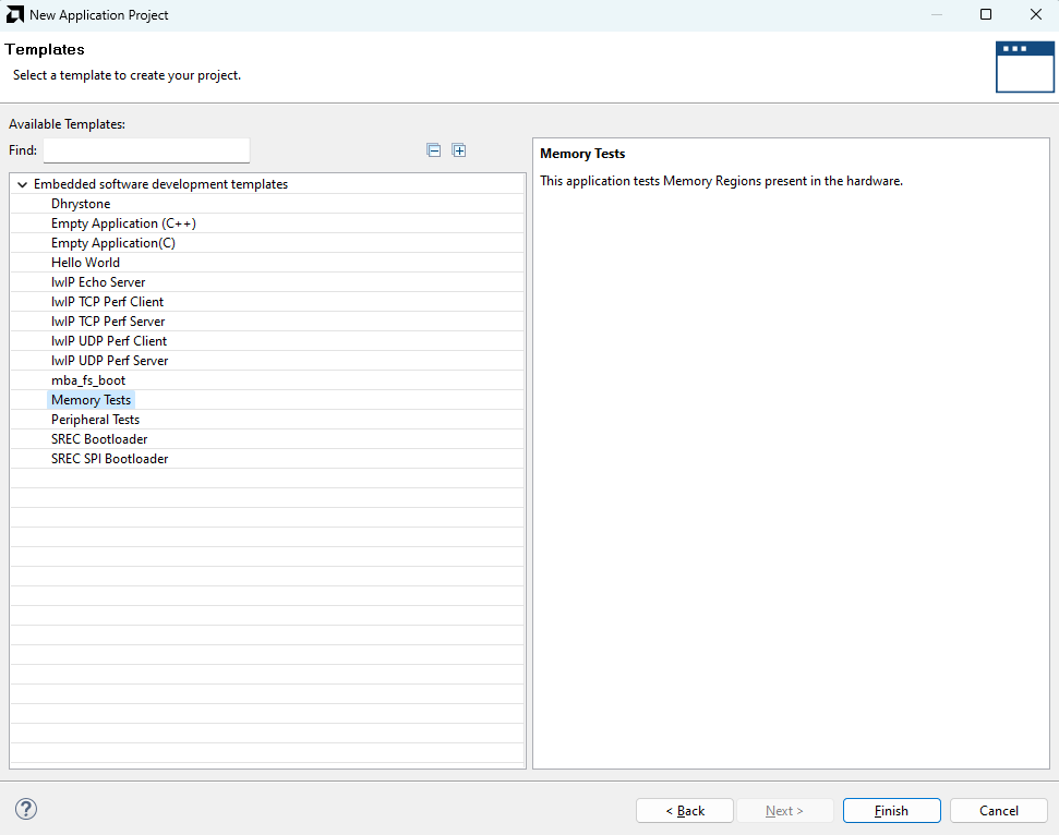
In the “Application Project Details” window, give an appropriate name for the Vitis Project and click “Next“. Click “Next” in the “Domain” window. Select the “Memory Tests” template from the list of available templates and click “Finish“.
Step 16:
Once the project is created, the Vitis will automatically run a build. If that didn’t happen for any reason, run the build manually. Once the build is completed successfully, power up Callisto Kintex 7 USB 3.1 FPGA Module and connect Xilinx Platform USB II JTAG cable and USB 3.0 Type-A to Type-C cable to the board.
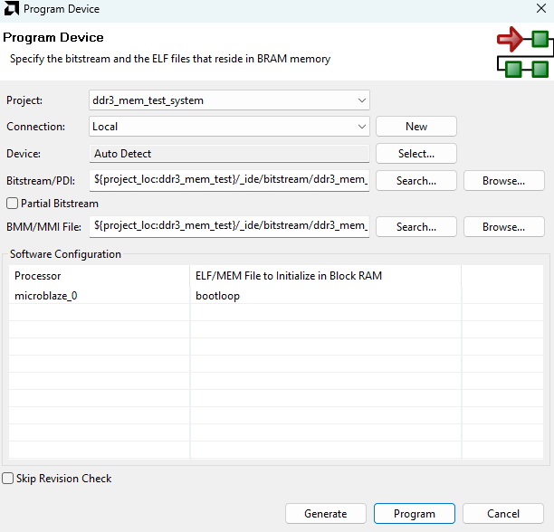
Step 17:
Program the FPGA on Mimas A7 Mini with a simple boot loop program by selecting the “Program Device” option from the “Vitis” menu.
Step 18:
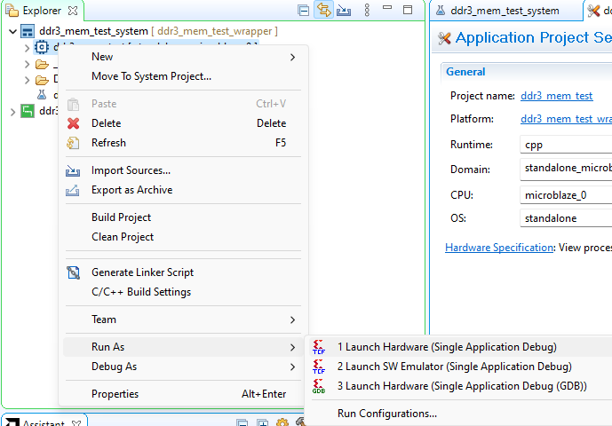
Now, right-click on the “.elf file” in Project Explorer and select “Launch Hardware” as shown below.
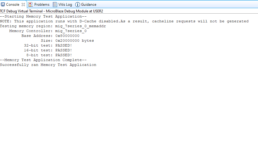
If everything went well, the memory tests application running on the board should start printing the memory tests over the JTAG UART and the output should be displayed in the Vitis Console terminal as shown in the image below.