Introduction:
Direct memory access (DMA) is a method that allows an input/output (I/O) device to send or receive data directly to or from the main memory, bypassing the CPU to speed up memory operations. Thus DMA enables more efficient use of interrupts, increases data throughput, and potentially reduces hardware costs by eliminating the need for peripheral-specific FIFO buffers. This article implements a simple design to demonstrate how to write and read data to Nereid Kintex 7 PCI Express Development Board which acts as a PCI Express endpoint device. Let’s get started!
Hardware required:
- Host PC with Linux or Windows (Linux preferred)
- Nereid Kintex 7 PCI Express FPGA Development Board
- Xilinx Platform Cable USB II (JTAG cable)
Software required:
- Vivado 2018.2 or higher
- RW-Everything (for Windows host)
Step 1:
Download and install Vivado Board Support Package files for Nereid from here. Follow the README.md file on how to install Vivado Board Support Package files for Numato Lab’s boards.
Step 2:
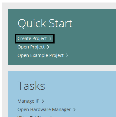
Open Vivado and select “Create Project” from the “Quick Start” section.
Step 3:
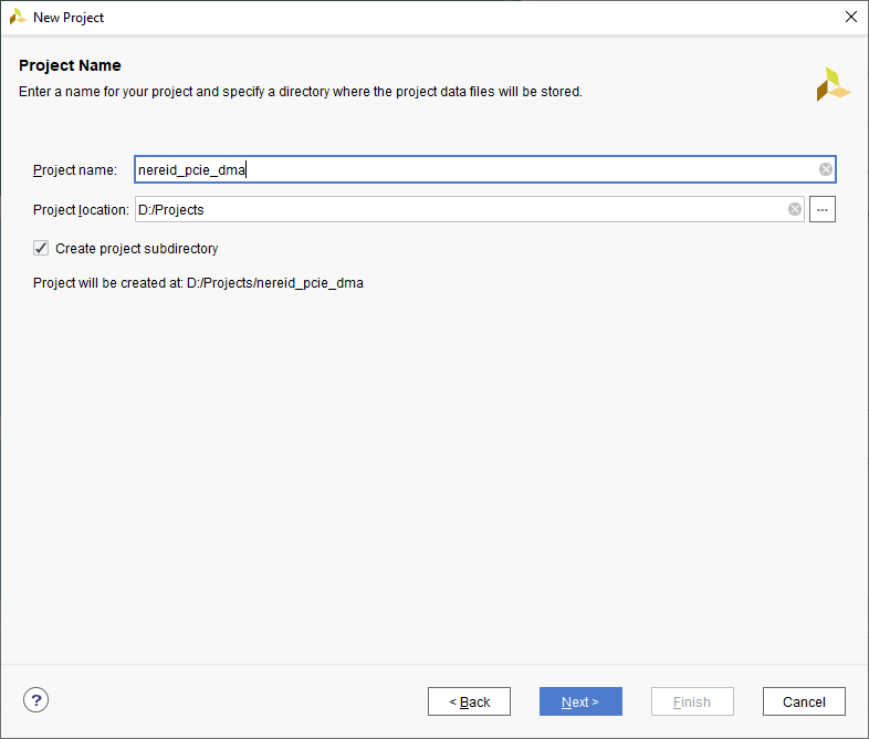
Click “Next” and then in the ‘Project Name’ tab, give the appropriate project name and location and click “Next” till you see the ‘Default Part’ tab.
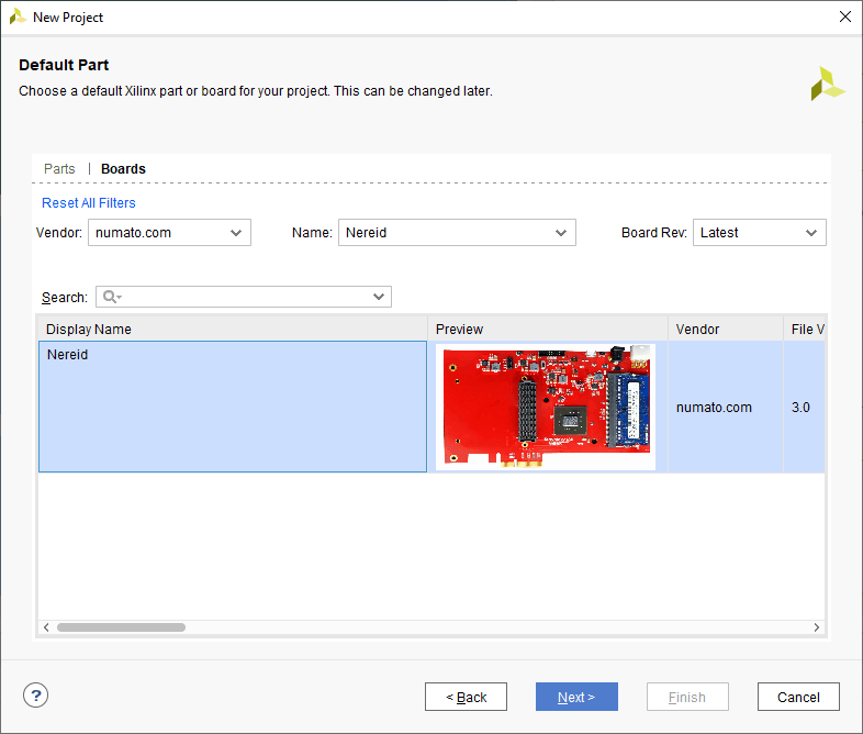
Step 4:
Select “Boards” from the “Default Part” tab, choose “numato.com” as Vendor. Select “Nereid” and click “Next”. If Nereid is not listed, make sure board support files are installed correctly. Click “Finish”. A new Vivado project will open with the selected settings.
Step 5:
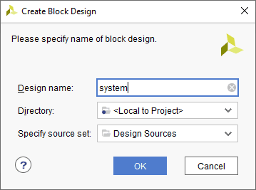
Click “Next” and then “Finish” to create the project. Click “Create Block Diagram” from the IP integrator tab on left, give a name for block design and click OK.
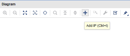
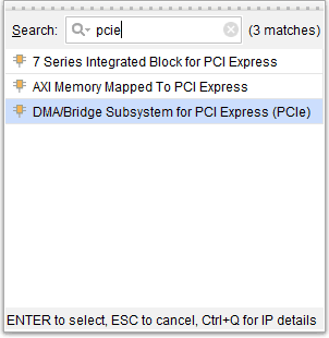
Step 6:
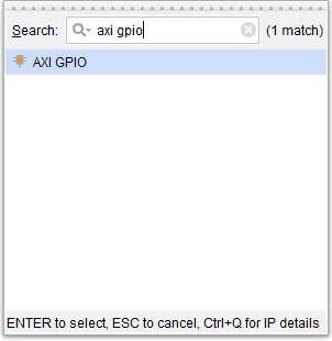
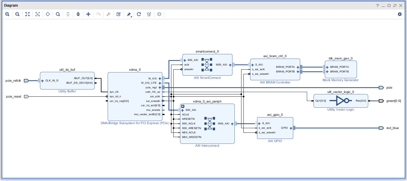
Click “Add IP” from the toolbar as shown in the image below. Type “PCIe” in the search box and double click on “DMA/Bridge Subsystem for PCI Express (PCIe)” to add the IP to the Block Design.
Step 7:
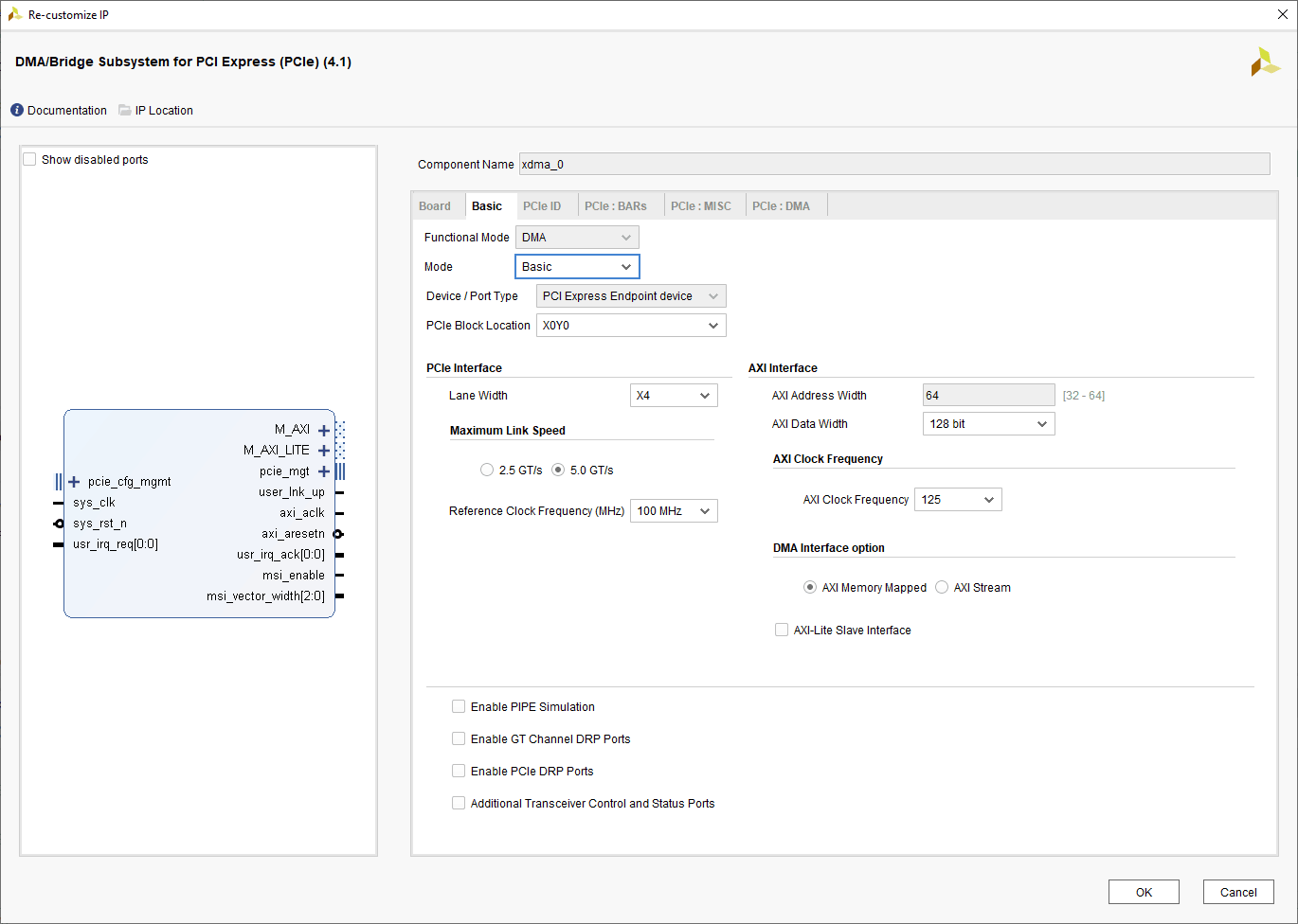
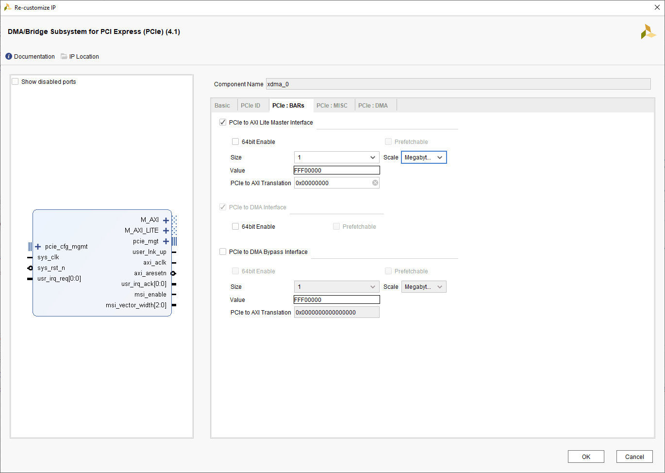
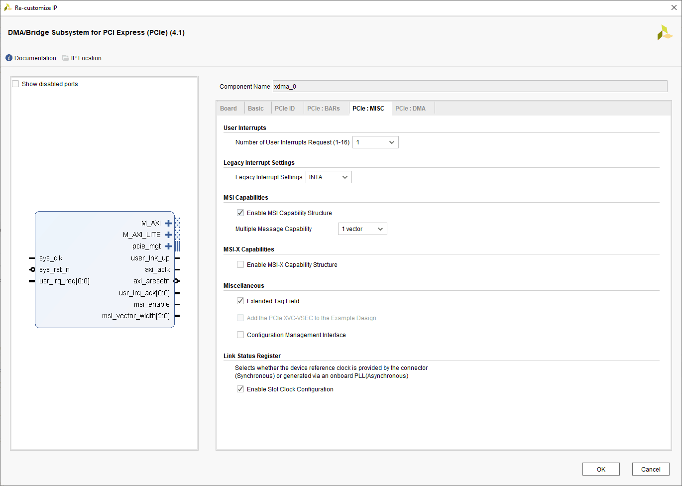
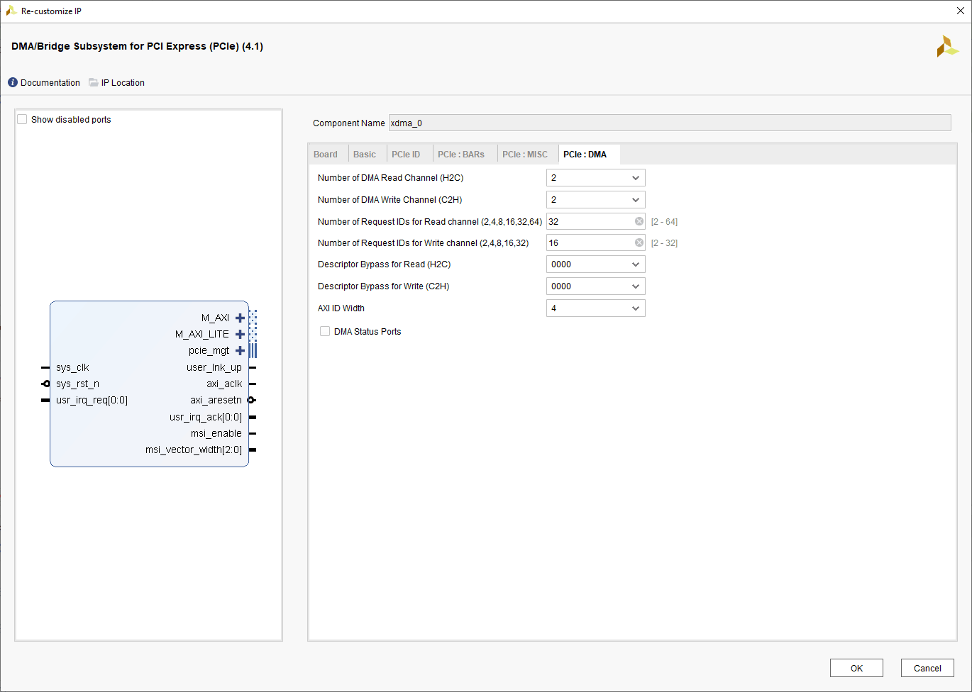
To customize the IP, double-click on the IP. The “Re-customize IP” window should open. In the Basic tab, Select “Lane Width” as “X4”, “Maximum Link Speed” as “5.0 GT/s”. In the “BARs” Tab, enable “PCIe to AXI Lite Master Interface” and set the Size Value as “1 Megabyte”. In the “Misc” tab, disable the “Configuration Management Interface” option and in the “DMA” tab, change the “Number of DMA Read Channel (H2C)” & “Number of DMA Write Channel (C2H)” to 2. Leave the other tabs in their default state and click OK. Refer to the images below for the settings mentioned in this step.
Step 8:
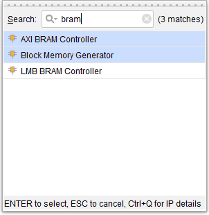
Now again click on “Add IP”, search for BRAM and double click on “AXI BRAM Controller” and “Block Memory Generator” to add the IPs to the design.
Step 9:
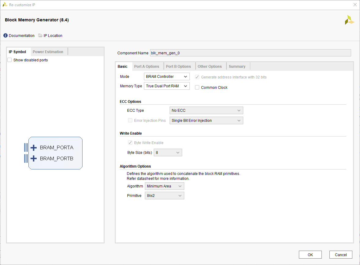
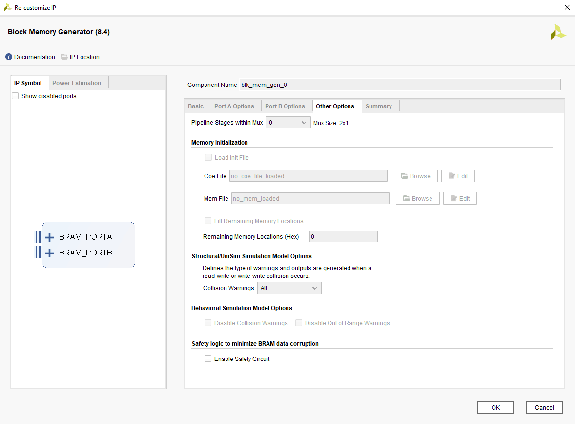
Now, double-click on the “Block Memory Generator” IP to customize it. Under the “Basic” tab, select the Memory Type as “True Dual-Port RAM”. In the “Other Options” tab, disable the “Enable Safety Circuit” option as shown in the images below.
Step 10:
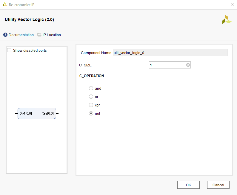
Click on “Add IP” and search for “Utility Vector Logic” and double click on the IP to add it to the design.

Double click on the IP to customize it. Change the “C_OPERATION” to “not” and change the “C_SIZE” to 1 and click “OK” as shown in the image below.
Step 11:
Now, add “AXI GPIO” IP to the design by clicking on “Add IP”.
To customize the IP, double click on the IP and in the Re-customization window that appears, under the “IP Configuration” tab, change the”GPIO Width” to 2 and enable the “All Outputs” option. The outputs of this IP are connected to Red and Blue LEDs of the board.
Step 12:
Now add the “‘AXI Smart connect” IP to the Block Design. Customize the IP to change the “Number of Slaves Interfaces” to 1.
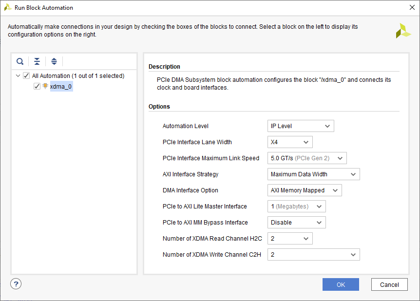
Now when all the required IPs are added to the design, connections should be made. For this, first click on “Run Block Automation” on the top left corner of the Diagram window as shown in the image below.

In the Run Block Automation window that appears, settings should be as shown below. Click “OK” for Vivado to automatically configure the blocks for you.
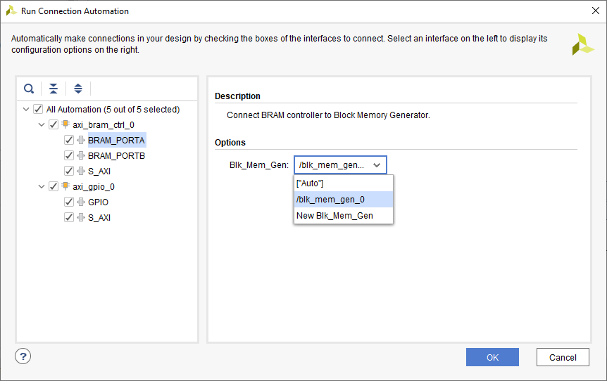
Once Block Automation is complete, run “Connection Automation” so Vivado can connect the blocks to make a complete system. In the Run Connection Automation window that appears, select the “BRAM_PORTA” interface and change the “Blk_Mem_Gen” under options to “/blk_mem_gen_0” as shown in the image below. Repeat the same for “BRAM_PORTB” and click “OK”.
Step 13:
Connect the input of Utility Vector Logic to “user_lnk_up” of “xdma_0” IP as shown in the image below (the highlighted connection in the below image).

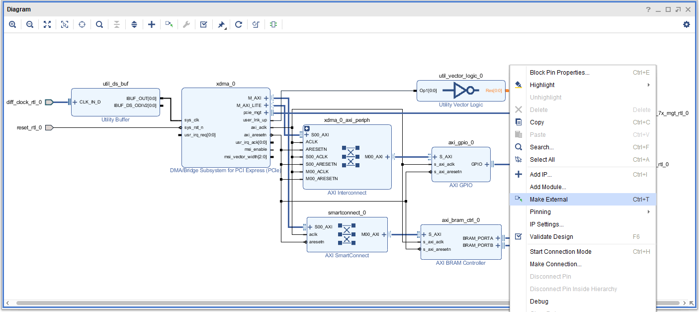
Now, right-click on the “Res[0:0]” pin of the Utility Vector Logic IP and select the “Make External” option to make the pin an output signal. This output port is connected to the Green LED of the board.
Step 14:
After all the above-mentioned steps for creating the design, the final Block Design should look like this: (change the port names accordingly)
Step 15:
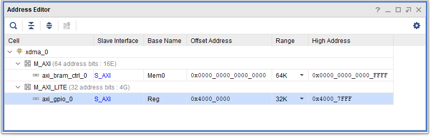
In the “Address Editor” tab, change the Offset Address and Range of axi_bram_ctrl_0 to “0x0000_0000_0000_0000” and “64K” respectively. Also, change the Range of axi_gpio_0 to “32K” as shown in the image below:
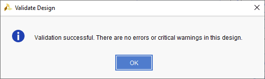
Validate the design to check if the block design has any errors. If the validation was successful, you should get a message as shown in the image below:
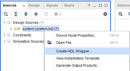
Now, save the block design and right-click on the design in the “Sources” window, select “Create HDL Wrapper” from the popup menu. Click “OK” on the window that appears to finish generating a wrapper.
Step 16:
We need to add constraints for the required ports. Since we have BSP, most of the ports would be assigned from the BSP. For a few ports, we will have to manually assign them.
To create an XDC file, click on the “+” button in the Sources tab.
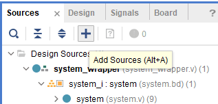
In the “Add Sources” window that appears, select “Add or create constraints” and click “Next” then select “Create File” and give any name for the XDC file, click OK and then Finish. Copy the below constraints and paste them into the XDC file.
set_property -dict {PACKAGE_PIN J26 IOSTANDARD LVCMOS33} [get_ports red_blue_tri_o[0]]
set_property -dict {PACKAGE_PIN H26 IOSTANDARD LVCMOS33} [get_ports green]
set_property -dict {PACKAGE_PIN G26 IOSTANDARD LVCMOS33} [get_ports red_blue_tri_o[1]]

set_property BITSTREAM.CONFIG.CONFIGRATE 16 [current_design]
set_property BITSTREAM.GENERAL.COMPRESS TRUE [current_design]
set_property BITSTREAM.CONFIG.SPI_BUSWIDTH 4 [current_design]
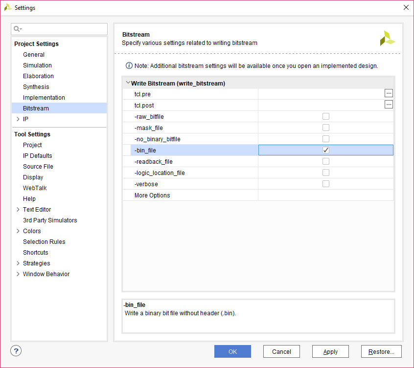
Step 17:
Now right click on “Generate Bitstream” under “PROGRAM AND DEBUG” in the “Flow Navigator” panel and select “Bitstream Settings”. Then enable the “-bin_file” option and click OK. Then click on Generate Bitstream to synthesis, implement and to generate the bitstream.
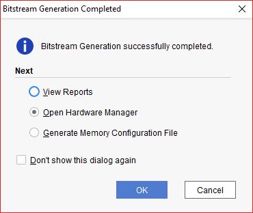
Step 18:
After successfully generating the bitstream, Open the Hardware Manager.
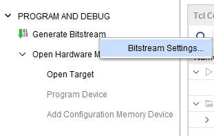
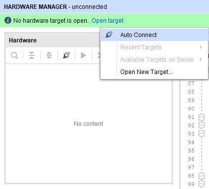
Step 19:
Make sure Nereid Board is connected to JTAG and power supply. Click on ‘Open target’ and ‘Auto-Connect’. Vivado Hardware Manager will connect to Nereid.
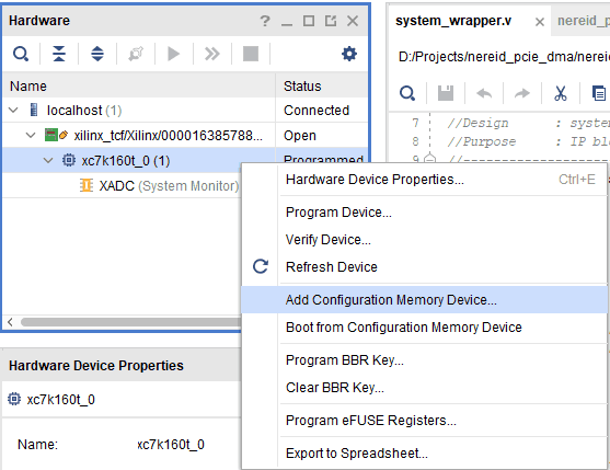
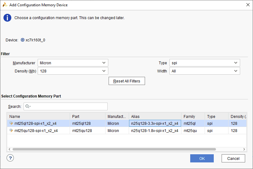
Step 20:
Left-click on the device and select ‘Add Configuration Memory Device…’. It will open a new window. Select Manufacturer as ‘Micron’, Density(Mb) as ‘128’ and Type as ‘spi’. Select device ‘mt25ql 128-spi-x1_x2_x4’ and click on OK.
Step 21:
A Dialogue window will appear asking if you want to program the configuration device now. Click Yes and program the .bin bitstream file which is located in “<project location>/ProjectName.runs/impl_1” directory.

Step 22:
Once the device is programmed, test it on a Windows or Linux machine.
Communicating with Nereid via PCI Express on Linux Machines:
To control the GPIOs (RGB LED connected in the design):
Step 1:
Download the complete pcimem application code zip file and unzip it in a specific location. Go to the command line terminal and check the PCIe base address by using the command.
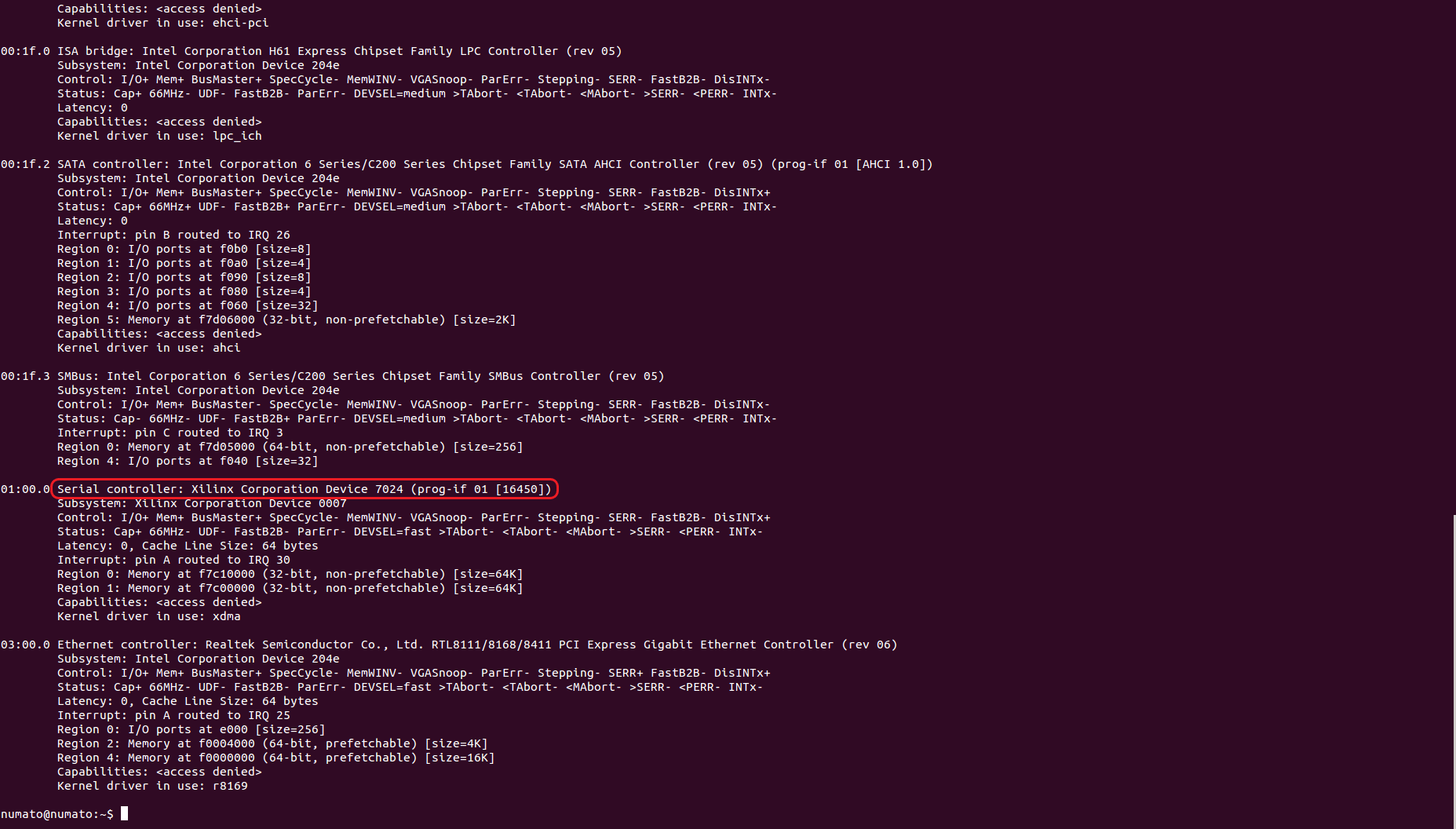
Go to the command line terminal and check if the PCIe device is being detected by the PC.
lspci -vv the output of the command is shown below. Make sure the Nereid Board is inserted correctly into the PCIe Slot of the host system’s motherboard. If the host is unable to detect Nereid (which should show up as “Serial controller: Xilinx Corporation Device 7024” as in the image below), make sure the board is inserted correctly into PCIe Slot and do a soft reset after the host is powered up. A soft-reset after the host is powered up helps the host detect FPGA-based PCIe devices.
Step 2:
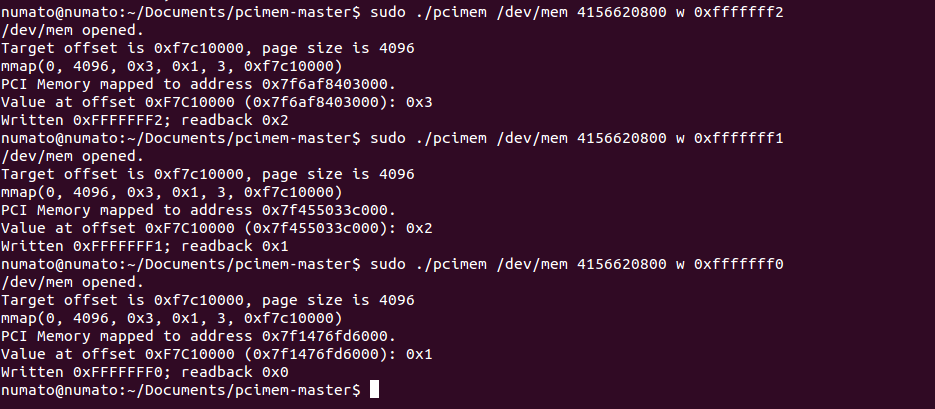
In the command-line terminal, open the path where you saved the ‘pciemem’ code. First, compile the C program by using the command “make”. Once it is compiled successfully, use the following command:
sudo ./pcimem /dev/mem 4156620800 w 0xfffffff2
Here,
4156620800: indicates the base address + offset, it is the address to which write is performed and it is the decimal value of hex: 0xf7c10000 .
w: indicates whether it is a word, a byte, or a half-word.
0xfffffff2: 32-bit data value for write purpose.
You will observe the following output indicating that the 32-bit data has been written to the specified address and read back from it. If the written data matches the data read, it means data was successfully written to Nereid and you will be able to observe the output on the LEDs. Here, the last 2 bits are taken for the output on RGB LED (in the above image).
To check the DMA functionality:
Step 1:
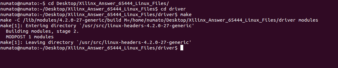
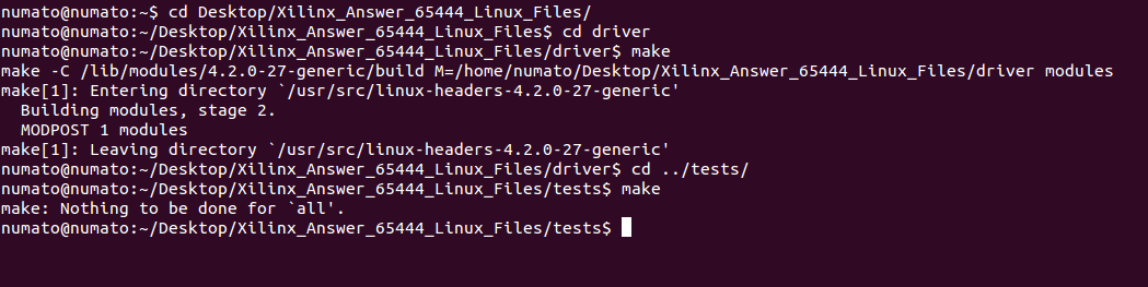
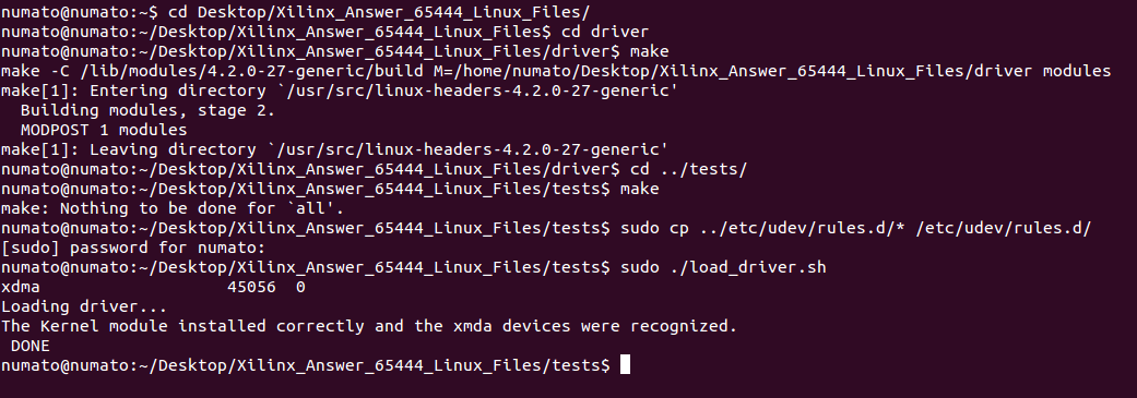
In the command-line terminal, open the path where you saved the ‘Xilinx_Answer_65444_Linux_Files’ folder. Enter the “driver” folder by using the command cd driver/ and compile the C program by using the command “make”. Once it is compiled successfully, use the following command cd ../tests/ to go to the “tests” folder and compile the C program by using the command “make”.
Step 2:
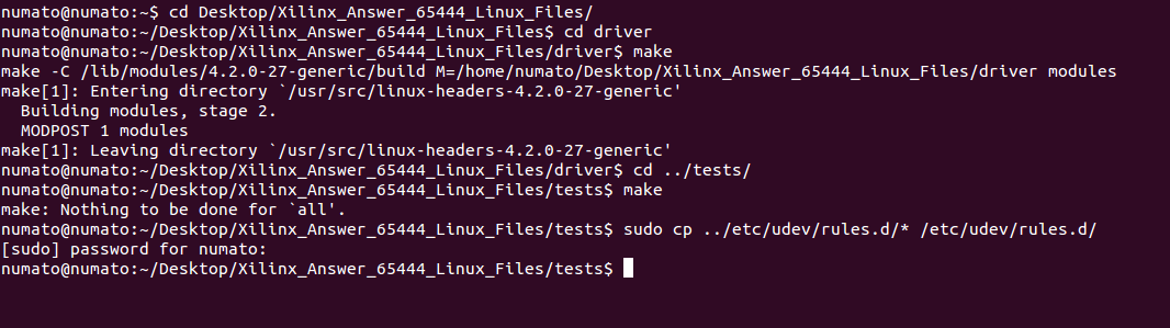
After compiling the codes, few files have to copy. To do this, use the following command: (as shown in the image below)
sudo cp ../etc/udev/rules.d/* /etc/udev/rules.d/
When this command is entered, you will be required to enter the password of the Linux User.
Step 3:
After the files are being copied, a driver has to be loaded onto the board. This can be done by using the following command:
sudo ./load_driver.sh
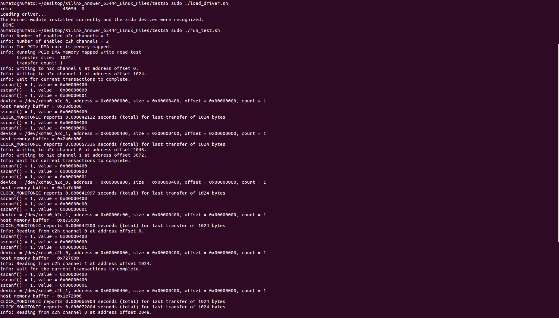
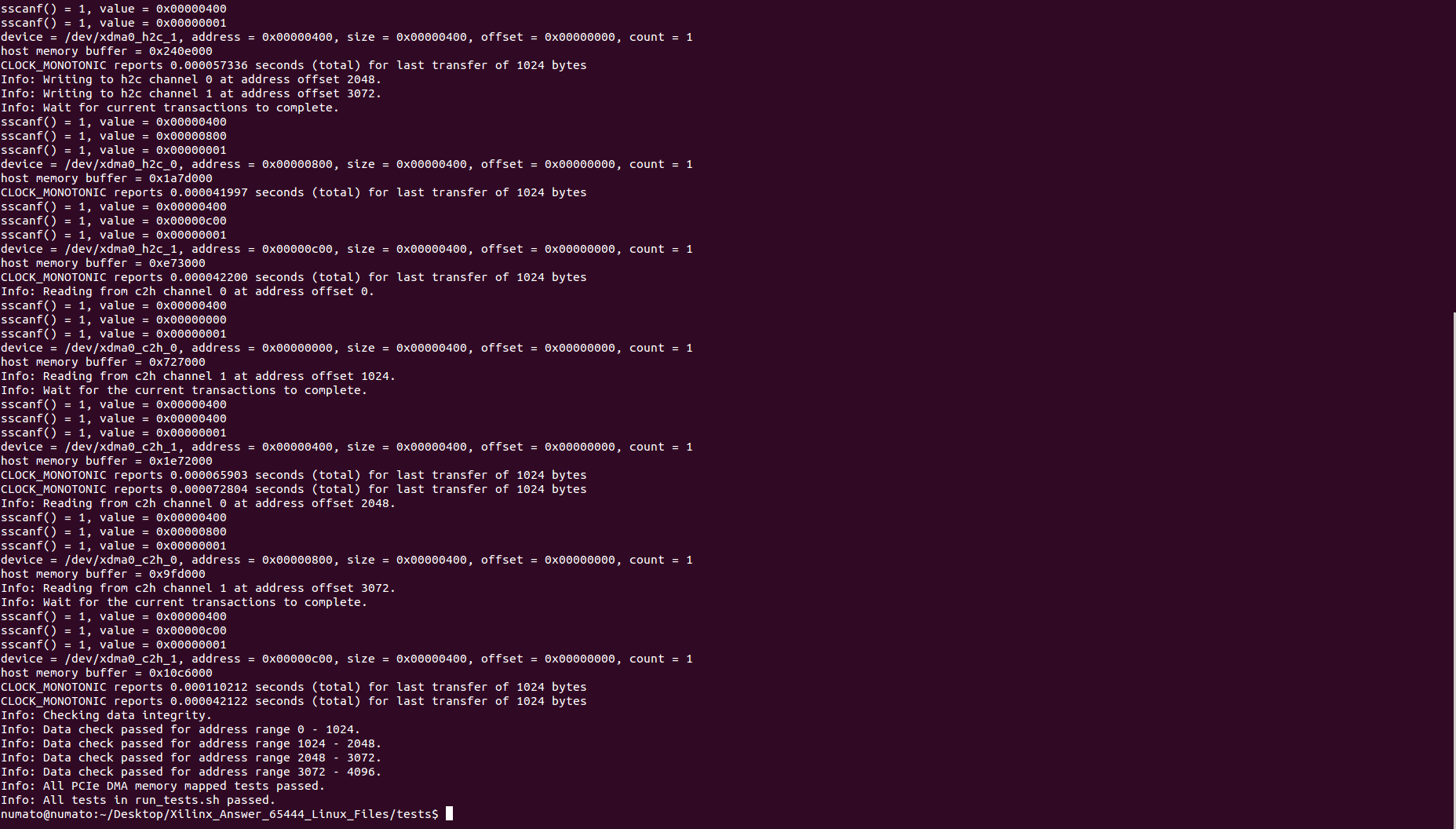
Step 4:
Once the driver is being loaded, we can now test the DMA. This can be done by running the script “run_test.sh”. If the tests in “run_tests.sh” pass without any errors, you will see a message that says “All tests in run_tests.sh passed.”. Use the following command to run the script:
sudo ./run_test.sh