Introduction
CPLD or FPGA and Which one to use? This is a common question that comes up very frequently especially among students and beginners. This article attempts to uncover some details of how they are different from each other and shed some light on the subject of which one to use. We will look at the advantages and disadvantages of each and discuss some situations where when one is suitable over the other.
CPLD Architecture
Let’s take a look at CPLD, Xilinx CoolRunner-II as a practical example. This is a very popular CPLD family manufactured by Xilinx. Below is a diagram that depicts Xilinx CoolRunner-II architecture.
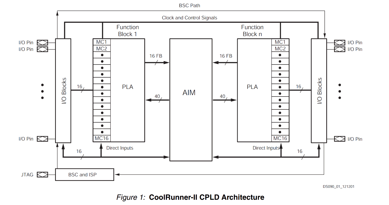
CoolRunner-II CPLD Architecture, Copyright: Xilinx Inc. Source: CoolRunner-II Datasheet
Let’s discuss a few features from the above image:
- This CPLD has few function blocks starting from “Function Block 1” to “Function Block n” (this number ranges from 2 to 32 in case of CoolRunner-II CPLDs)
- 16 lines of output from each Function Block go into AIM (Advanced Interconnect Matrix), whereas 40 lines of signals are input into Function Blocks from the AIM.
- Each function block has 16 MacroCells (MC1 to MC16).
- Each MacroCell has access to 16 signals from I/O Blocks
- Structure of MacroCell is shown below. Each macrocell contains 1 Flip-Flop and PLA array of Sum of Products which users can utilize to create to combinatorial or sequential logic. So the maximum number of Flip Flops available in CoolRunner-II CLPD (XC2C512) is 512! (Remember this number, we will compare it with a number of Flip Flops in FPGAs)
- The AIM can be programmed to interconnect the signals as we want. But as we saw in the second bullet point above, the number of signals is limited for each function block.
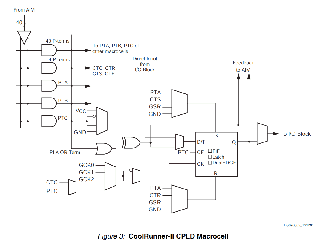
CoolRunner-II CPLD Macrocell, Copyright: Xilinx Inc. Source: CoolRunner-II Datasheet
Same as in PLAs, CPLDs’ logic function in each Macrocell are electrically programmed via In System Programming (ISP) Interface over JTAG (check Figure 1). After programming, these flash-based connections remain persistent for years. This gives CPLDs a unique advantage of “instant-on” working. That is, CPLDs start working as soon as powered up since their circuitry is flashed/burned into them via ISP. That is not the case with FPGAs as we will see later.
Generalizing, we can say that, in CPLDs, there are a few hundred function blocks (or logic blocks), typically less than a thousand in number, which are accessible by a single big interconnect.
FPGA Architecture
While the exact FPGA architecture is not publicly released by manufacturers, we can still get higher level architecture, which will help in understanding FPGAs and its working. A high-level example from Xilinx’s documentation is below.

FPGA Architecture: CLB and Interconnect. Copyright: Xilinx Inc. Source
In the case of FPGAs, there are many Configurable Logic Blocks (CLBs) embedded in an ocean of programmable interconnects. These CLBs are incredibly complex compared to Macrocells of CPLDs and can implement vastly more complex logic functions. They are primarily made of Look-Up Tables (LUTs), Multiplexers and Flip-Flops. For the brave, Xilinx published a lot of details in Xilinx User Guide on 7 Series FPGAs Configurable Logic Block. FPGAs can contain even millions of CLBs in a single device! And millions of Flip-Flops (~3.456 million Flip Flops in Xilinx VU13P)! Compare that with just 512 Flip-Flops in the biggest CPLD from Xilinx! In short, FPGAs are massive! (not all but many are)
Specialized hardware on FPGA. Copyright: Xilinx Inc. Source
As illustrated above, FPGAs also have dedicated hardware for various functions such as RAM, High-Speed Serial Transceivers, Digital Signal Processing (DSP) Blocks, External Memory Controllers, PLLs and MMCMs, PCIe, etc! In terms of variety of choices and flexibility, CPLDs are no match for FPGAs.
As mentioned before, FPGAs are LUT based. When an FPGA is powered up, the device is always blank. A special circuit called Configuration Circuit is present which reads the configuration data from an external ROM, and configures the LUTs as per user’s design present in the external ROM. It takes some time for FPGA to get configured and the FPGA will start functioning only after configuration loading is complete. There certainly are exceptions to this. Some manufacturers have come up with FPGAs that have built-in configuration flash. Even in this case, the configuration data is not embedded in the fabric and some amount of configuration/setup time still apply.
CPLD vs FPGA comparison summary
| No. | CPLD | FPGA |
|---|---|---|
| 1 | Instant-on. CPLDs start working as soon as they are powered up | Since FPGA has to load configuration data from external ROM and setup the fabric before it can start functioning, there is a time delay between power ON and FPGA starts working. The time delay can be as large as several tens of milliseconds. |
| 2 | Non-volatile. CPLDs remain programmed, and retain their circuit after powering down. FPGAs go blank as soon as powered-off. | FPGAs uses SRAM based configuration storage. The contents of the memory is lost as soon as power is disconnected. |
| 3 | Deterministic Timing Analysis. Since CPLDs are comparatively simpler to FPGAs, and the number of interconnects are less, the timing analysis can be done much more easily. | Size and complexity of FPGA logic can be humongous compared to CPLDs. This opens up the possibility less deterministic signal routing and thus causing complicated timing scenarios. Thankfully implementation tools provided by FPGA vendors have mechanisms to assist achieving deterministic timing. But additional steps by the user is usually necessary to achieve this. |
| 4 | Lower idle power consumption. Newer CPLDs such as CoolRunner-II use around 50 uA in idle conditions. | Relatively higher idle power consumption. |
| 5 | Might be cheaper for implementing simpler circuits | FPGAs are much more capable compared to CPLDs but can be more expensive as well. |
| 6 | More "secure" due to design storage within built in non-volatile memory. | FPGAs that use external memory can expose the IP externally. Many FPGA vendors offer mechanisms such as encryption to combat this. Design specific protection mechanisms also can be implemented. |
| 7 | Very small amount of logic resources. | Massive amount logic and storage elements, with which incredibly complex circuits can be designed. FPGAs have thousands times more resources! This point alone makes FPGAs more popular than CPLDs. |
| 8 | No on-die hard IPs available to offload processing from the logic fabric. | Variety of on-die dedicated hardware such as Block RAM, DSP blocks, PLL, DCMs, Memory Controllers, Multi-Gigabit Transceivers etc give immense flexibility. This is not even thinkable with CPLDs. |
| 9 | Power down and reprogramming is always required in order to modify design functionality. | FPGAs can change their circuit even while running! (Since it is just a matter of updating LUTs with different content) This is called Partial Reconfiguration, and is very useful when FPGAs need to keep running a design and at the same time update the it with different design as per requirement. This feature is widely used in Accelerated Computing. |
| 10 |
Where to use CPLD or FPGA
When a design requires simple glue-logic or similar functionality which doesn’t need to be changed much, or when you need an instant-on circuit, then go for CPLDs. Otherwise, for most other applications FPGAs are generally preferred. Sometimes you can find both CPLD + FPGA in a design. In those designs, CPLDs generally do simple glue-logic as mentioned before, and are responsible for “booting” the FPGA as well as controlling reset and boot sequence of a complete board. So, depending on the application you might need to use both in a particular design.
So, there you go! We hope that you are now more enlightened about CPLDs vs FPGAs and can make an informed decision on which one to use depending on your application needs. The module form-factor boards such as the Narvi Spartan 7 FPGA Module make it easier to implement the applications without requiring end-product designers to take care of complex details such as FPGA power supplies, DDR3 routing, etc. Feel free to browse our wide range of FPGA Boards to prototype and develop your applications.