Introduction
The Vivado Design Suite is a comprehensive development environment from Xilinx, designed to streamline the design, integration, and implementation of systems using Xilinx UltraScale, 7 series devices, and the Zynq-7000 family. With powerful tools like the IP Integrator and seamless integration with Vitis for software development, Vivado enables rapid prototyping and efficient design workflows. In this article, we’ll walk through creating a simple “Hello World” project on the Mimas AU-Plus FPGA Board, using a 32-bit MicroBlaze soft processor and AXI4-connected peripherals.
What is MicroBlaze?
MicroBlaze is a 32-bit soft processor IP developed by Xilinx for their mid and high-end FPGA devices. It is compatible with Xilinx’s Ultrascale+, 6 and 7 series FPGAs. More information on MicroBlaze can be found on Xilinx’s MicroBlaze page. Advanced knowledge of MicroBlaze or AXI is not a prerequisite to follow this article. Thanks to the excellent tools provided by Xilinx, most of the design can be done without writing any code at all.
What is AXI?
AXI stands for Advanced eXtensible Interface. AXI is a bus interconnect based on ARM’s popular AMBA bus architecture. In a MicroBlaze system, AXI connects the microprocessor to all peripherals in the system. The only exception is the Block RAM which is attached to the processor through the LMB (Local Memory Bus). AXI4-Lite is available for connecting low throughput peripherals to the system such as the UART, GPIO, etc. AXI4-Lite uses fewer logic resources on FPGA compared to AXI. Usually, AXI is used to connect high throughput peripherals such as DDR memory, Ethernet, etc. Again, a detailed understanding of AXI is not required for following this article. But for curious readers, AXI Reference Guide is available here.
Mimas AU-Plus FPGA Board
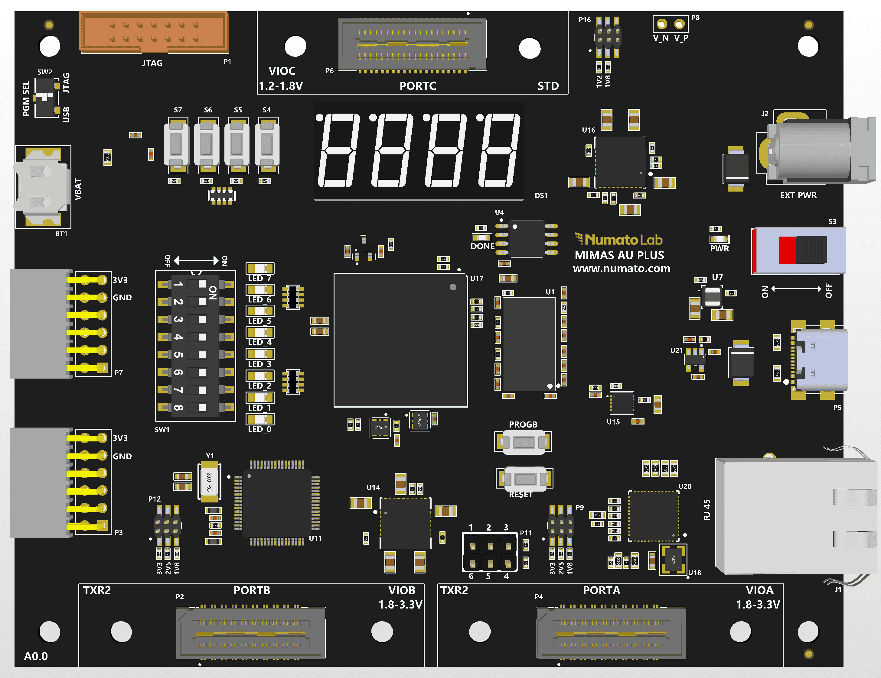
The Mimas AU-Plus FPGA Board from Numato Lab is an Artix Ultrascale+ FPGA (XCAU7P-1SBVC484 package). The FT2232H brings versatile USB-to-serial connectivity, while DDR4 support enhances data processing efficiency. The inclusion of Gigabit Ethernet facilitates seamless networking, opening doors to IoT and cloud computing applications. Storage is swift and reliable with QSPI flash, while the M.2 M key interface embraces cutting-edge storage solutions and supports high-speed communication. The addition of PMOD connectors enhances flexibility, allowing easy interfacing with sensors and peripherals for customized project. Let’s get started!
Prerequisites:
Hardware:
- Mimas AU-Plus FPGA Board
- Xilinx Platform Cable USB
- USB type C cable
Software:
- Vivado Design Suite 2025.1
- Vitis Unified IDE 2025.1
- Serial Terminal (PuTTY, Tera Term, etc.)
Creating MicroBlaze based Hardware Platform for Mimas AU-Plus
The following steps will walk you through the process of creating a new project with Vivado and building a hardware platform with a MicroBlaze soft processor using the Vivado IP integrator. Screenshots are added wherever possible to make the process easier for the reader.
Step 1:
Download and install the Vivado Board Support Package files for Mimas from here (change the bsp). Follow the README.md file on how to install Vivado board support files for Numato Lab boards.
Step 2:
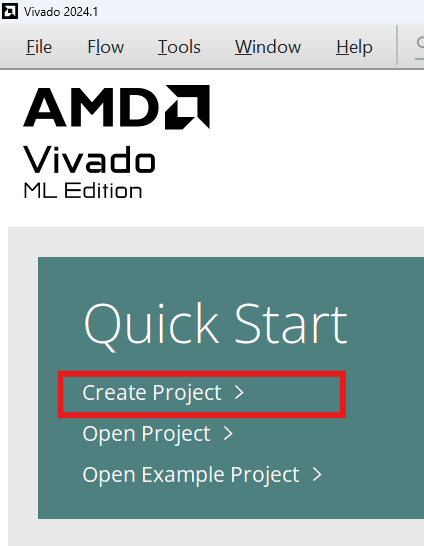
Start Vivado Design Suite, and select “Create Project” from Quick Start section. The project wizard will pop up. Press “next” to proceed with creating the project.
Step 3:
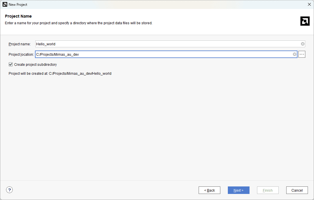
In the “Project Name” window, enter a name for the project and save it at a suitable location. Select the option “Create project subdirectory” to keep all the project files in a single folder and click “Next” without making any changes until you see the “Default Part” page.
Step 4:
In the “Default Part” window, select the “Boards” tab. Choose the Vendor as “numato.com”, filter the Name “Mimas_AU_Plus” and select the board as shown below. If Mimas_AU_Plus is not displayed in the Boards list, make sure that the board support files (change the bsp) are installed correctly.
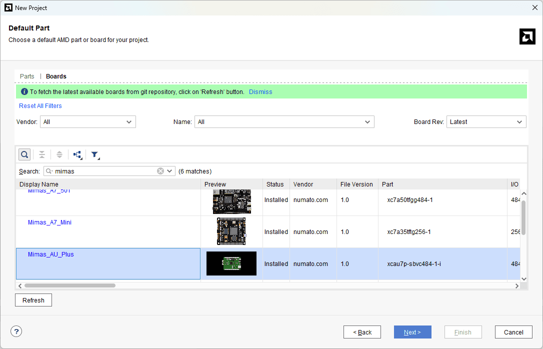
Click “Next” to continue. On the next page, click “Finish” to complete creating a new project. A new project will be created by Vivado with the selected settings.
Step 5:
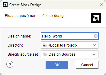
Under the “Flow Navigator” panel, click “Create Block Design” under the IP Integrator section. Enter a name for the block design and click “OK”.
An empty block design will be created.
Step 6:
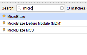
As shown in the “Diagram” window, click the “Add IP” icon, search for MicroBlaze and add it to the design by double-clicking its name in the list.
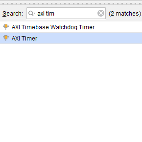
 Add AXI Timer to the block design.
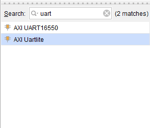
Similarly, add AXI Uartlite to the block design.
Step 7:
Click the “Board” tab. The default peripherals available for the Aller board will be listed as shown below.
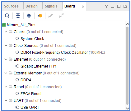
Drag and drop the System Clock, FPGA Rest and DDR4 peripherals into the block design.
Step 8:
Click “Run Block Automation” and change the settings as shown below. Also, enable the “Interrupt Controller” checkbox.
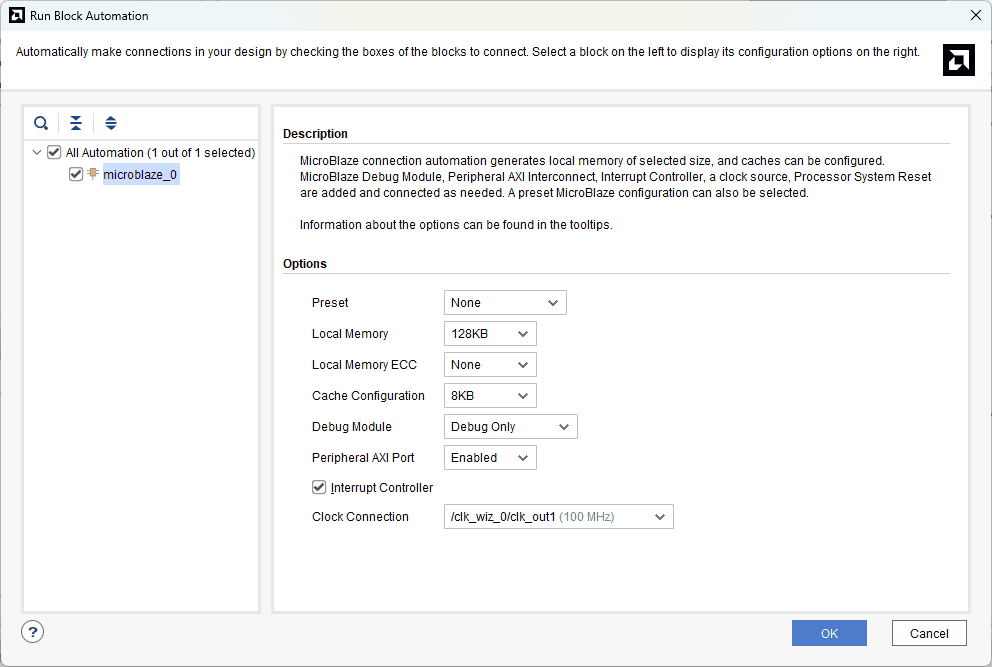
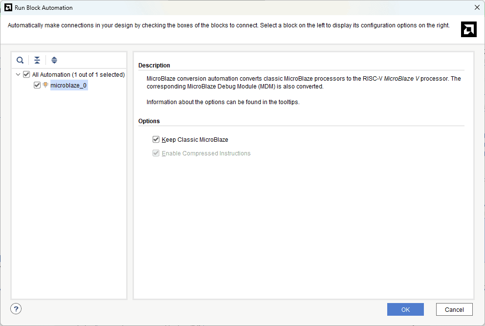
Click “OK” for Vivado to automatically configure the blocks for you. In Vivado 2025.1 after clicking on “OK” a window will appear, here you need to select “Keep Classic MicroBlaze” and then click OK to use Microblaze.
Step 9:
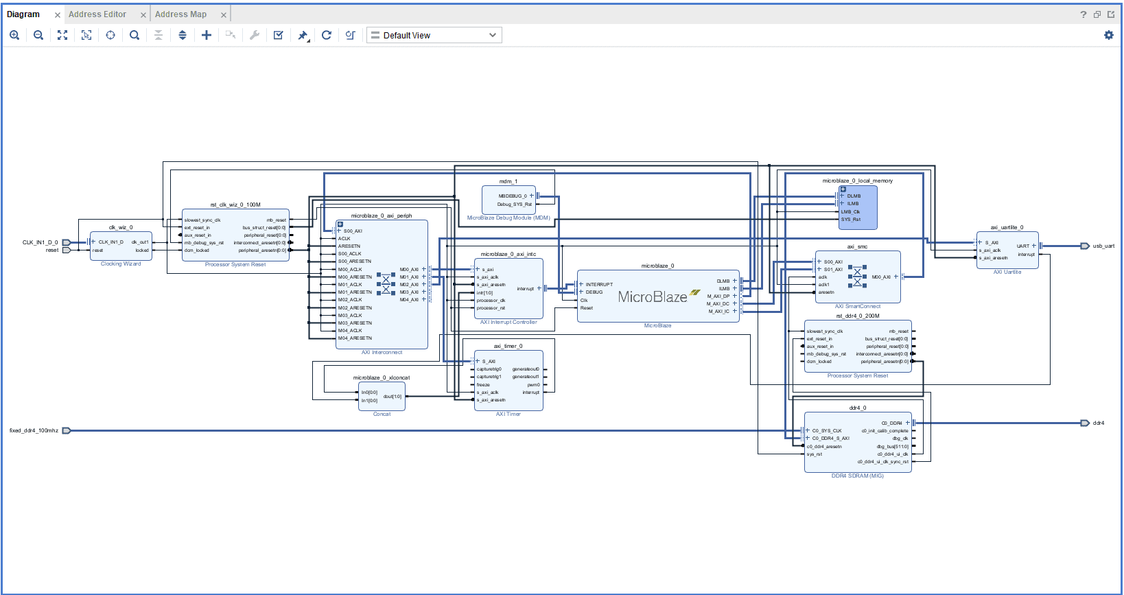
Once Block Automation is complete, run “Connection Automation” so Vivado can connect the blocks to make a complete system. Connect interrupt output lines from “AXI Timer” and “UARTLite” to the “Concat” block as shown below figure. Select the “Validate Design” option from the Tools menu to make sure that connections are correct.
Step 12:
Right-click “Hello_world” in the “Sources” window, and select “Create HDL Wrapper” from the popup menu. Click “OK” on the window that appears to finish generating a wrapper.

Step 13:
Click “Generate Bitstream” under the “Program And Debug” section to synthesize, implement and generate a bitstream.

Step 14:
After generating the bitstream successfully, select Export -> Export Hardware from the File menu. Click Next.

Select the “include bitstream” checkbox and click Next.

Provide the XSA file name and save it at a suitable location. Click Next and click Finish in the next dialog box.

Step 15:
Launch Vitis IDE and create a new platform for the project, by selecting “Create Platform Component”, click “Next”, in the Flow tab select the XSA file saved using the step 15 and finally click “Next” and “Finish” respectively.

Step 16:
Give the component name and the platform location and click on “Next”.

Step 17:
In the next tab browse the XSA file , select it , click on “Next”. In the next OS and Processor tab click “Next” and “Finish”.

After successful creation of the platform, build the platform.

Step 18:
Next create the Hello world Application component by selecting the “Hello world” template from the “examples”.

In “Create Application Component” tab specify project name and location, click “Next”.

Select newly created Platform and click “Next”.

Select the domain as “Standalone_microblaze_0” and click “Next” and click on “Finish”.

When the Hello world project is added successfully, build the project manually.

Step 19:
Once the build is completed successfully, power up Mimas AU plus FPGA Development Board using USB type C cable and connect the JTAG cable for programming the device.
Step 20:
Program the FPGA on Mimas AU Plus with a simple boot loop program by selecting the Program Device option from the Vitis menu.

Once the “Program Device” window opens give the path for .bit and .mmi files .
If the “BMM/MMI” File is not selected , manually browse and select the file .Once the files are selected click on “Program” .

Step 21:
Meanwhile, open any serial terminal program (such as PuTTY, Teraterm etc) and open the port corresponding to Mimas AU plus with a 9600 baud rate (the default baud rate given in UART IP). Program the board by selecting the “Run”.

Step 22:
If everything went well, the application running on the board should print “Hello World” over the UART and should be displayed on the Serial Terminal application.
