Introduction
Vivado Design Suite by AMD is used for synthesis and analysis of HDL designs with additional features for SOC development and high-level synthesis. AMDrecommends use of Vivado Design Suite for new designs with Ultra scale, Virtex-7, Kintex-7, Artix-7 and Zynq-7000. Complete pack of Vivado Design Suite contains Vivado High-Level Synthesis, Vivado Simulator, Vivado IP Integrator and Vivado TCL Store. We will be using Vivado IP Integrator alongside Vitis to create our “Hello World” project for Neso Artix 7 FPGA Module. The design will contain a Microblaze soft processor and peripherals connected together by AXI bus. Thanks to the excellent tools provided by AMD, most of the design can be done without writing any code at all.
What is Microblaze?
Microblaze is a 32 bit soft processor IP developed by AMD for their mid – high end FPGA devices. Microblaze is compatible with AMD’s 6 and 7 series devices such as Spartan 6, Artix, Kintex, Virtex and Zynq devices. More information and resources including datasheet for Microblaze can be found at AMD’s Microblaze page. Microblaze IP is bundled with AMD IP integrator. Microblaze based embedded design can use either PLB or AXI as the bus system.
What is AXI?
AXI stands for Advanced eXtensible Interface. AXI is a bus interconnect based on ARM’s popular AMBA bus architecture. In a Microblaze system AXI connects the microprocessor to all peripherals in the system. The only exception is Block RAM which is attached to the processor through LMB (Local Memory Bus). AXI Lite is available for connecting low throughput peripherals to the system such as UART, GPIO etc.… AXI Lite uses less logic resources on FPGA compared to AXI. Usually AXI is used to connect high throughput peripherals such as DDR memory, Ethernet etc… Again, a detailed understanding of AXI is not required for following this article. But for the curious readers, AXI Reference Guide is available here.
Neso Artix 7 FPGA module is the first product in a series of AMD 7 Series FPGA based products. Neso is pin compatible with Numato Lab’s Saturn Spartan 6 FPGA module and can replace Saturn with no hardware changes in most cases. Neso offers built in USB interface that can be used to program the board as well as do debugging or data transfer with the host. With a XC7A100T FPGA on board, Neso is a great choice for learning, product development and OEM integration.
Neso Artix 7 FPGA Module Specification
| FPGA Device: | XC7A100T – CSG324 |
| Memory Type: | DDR3 |
| Memory Size: | 2GBits |
| Number Of GPIOs (Max): | 140 |
| Configuration Options: | JTAG, USB |
| Primary Clock Frequency: | 100MHz |
Tools and Prerequisites
- Neso Artix-7 Development Board.
- Vivado Design Suite and Vitis (Version 2025.1)
- AMD Platform Cable USB II.
- FT_Prog tool for configuring on-board FT2232H USB Serial converter (download and install from FTDI website).
Creating Microblaze based Hardware Platform for Neso
The following steps will walk you through the process of creating a new project with Vivado and building a hardware platform with Microblaze soft processor using IP integrator. Numato Lab’s Neso Artix 7 FPGA Module is used in this example but any compatible FPGA platform can be used instead with minor changes to the steps. Screenshots are added wherever possible to make the process easier to the reader.
Step 1:
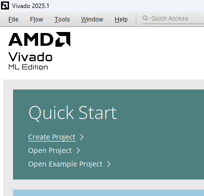
Start Vivado Design Suite, and select “Create Project” from Quick Start section. The project wizard will pop up. Press next to proceed with creating the project.
Step 2:
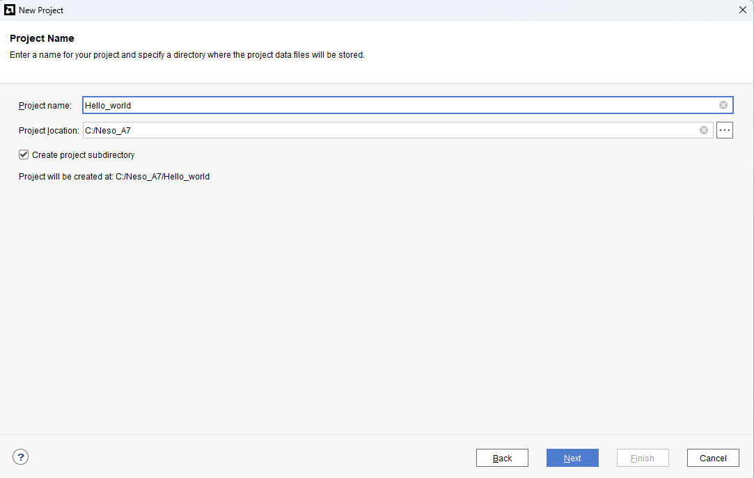
Enter a name for the project and save it at a suitable location. Check the option “Create project subdirectory”. Click Next to continue.
Step 3:
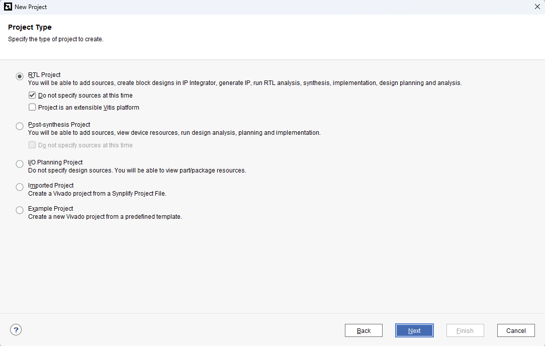
In the Project Type window, select RTL Project and check the option “Do not specify sources at this time”. Click Next.
Step 4:
At the “Default Part” stage, switch to the “Boards” tab and set the vendor to numato.com. Select “Neso” and click Next.If the Neso board does not appear in the list, click “Refresh” to update the board catalog. Vivado will then download the latest board files, after which Neso will become available for selection.
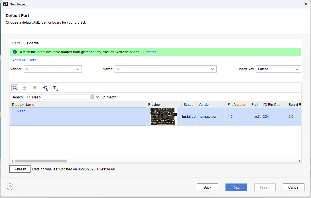
Click Finish to complete creating a new project. A new project will be created by Vivado with the selected settings.
Step 5:
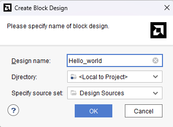
In the Flow Navigator panel, select Create Block Design under IP INTEGRATOR. Enter a name for the block design and click OK. An empty block design will be created.
Step 6:
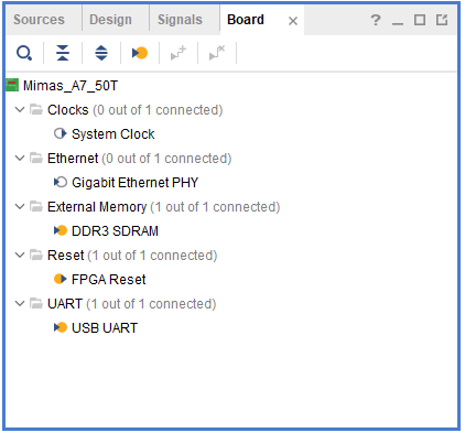
Click the Board tab. The default peripherals available for the Neso A7 board will be displayed.
Step 7:
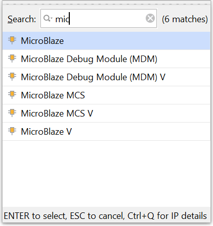
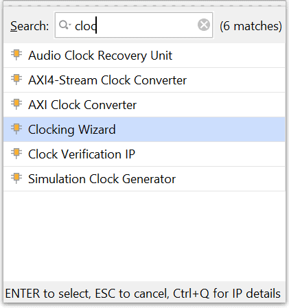
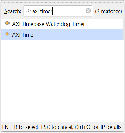
Add DDR3 SDRAM and USB UART to the design by double-clicking the corresponding peripherals. In the Diagram window, right-click and select “Add IP” from the popup menu. Search for “MicroBlaze” ,”clocking wizard” & “AXI Timer” and add them to the design by double-clicking them.
Step 8:
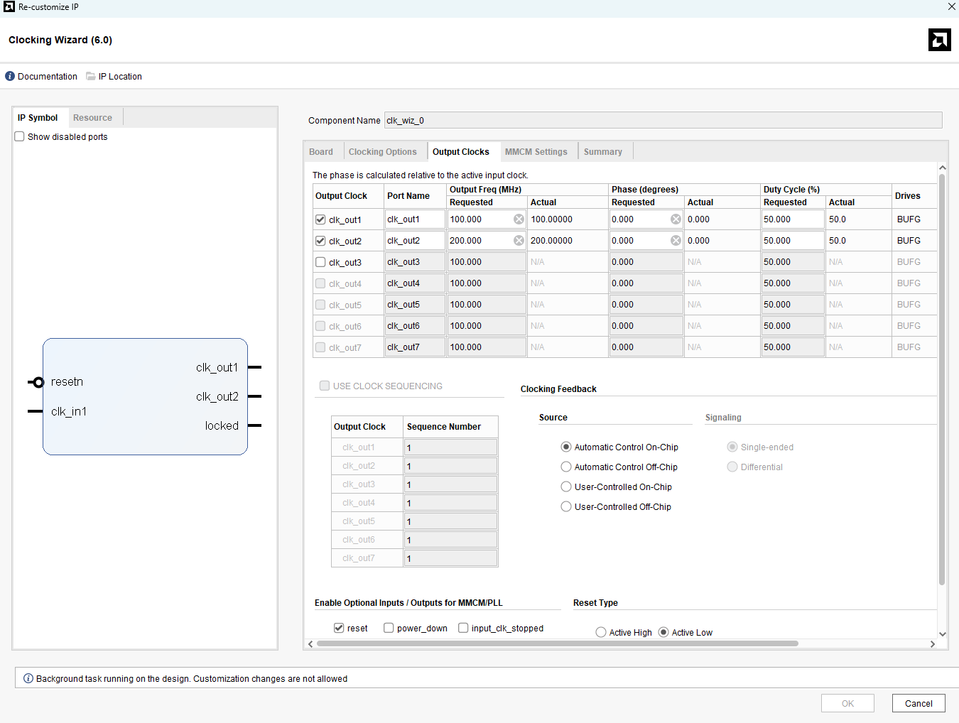
Double click “Clocking Wizard” IP and customize “Output Clocks” settings as shown in the following image.
Step 9:
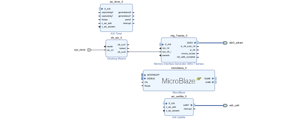
Remove existing “sys_clk_i” connection and input port (if any) and connect “clk_out2” net on the clocking Wizard to “sys_clk_i” of “MIG 7 Series” block as shown in the following image.
Step 10:
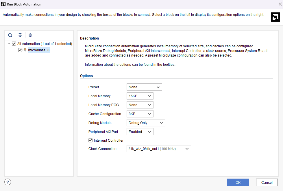
Click “Run Block Automation” present in the “Designer Assistance available” bar on the top left corner of the window to complete the design. Select the settings as shown in the following image. Click “OK” for Vivado to automatically configure the blocks for you. Once Block Automation is complete, run “Connection Automation” so Vivado can connect the blocks together to make a complete system.
Step 11:
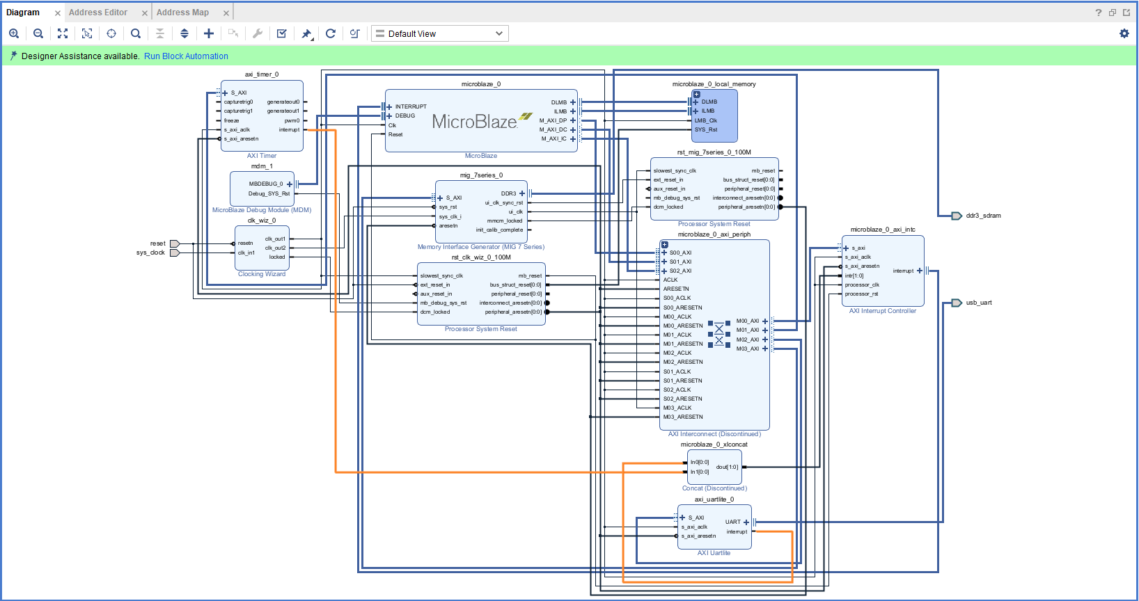
Connect interrupt output lines from AXI Timer and UartLite to the Concat block as shown in the picture below. The connections are highlighted in orange.
Step 12:
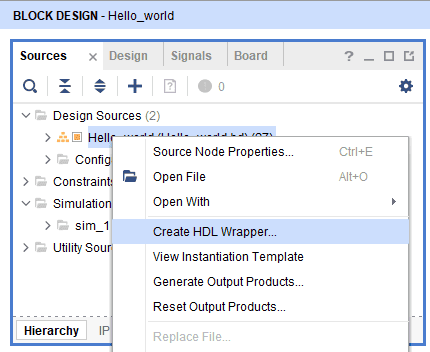
Right-click on the design in the “Sources” window, select “Create HDL Wrapper” from the popup menu. Click “OK” on the window that appears to finish generating a wrapper.
Step 13:
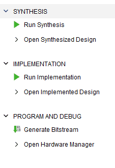
Double click on “Generate Bitstream” under “Program And Debug” section to synthesize, implement and generate the bitstream.
Step 14:
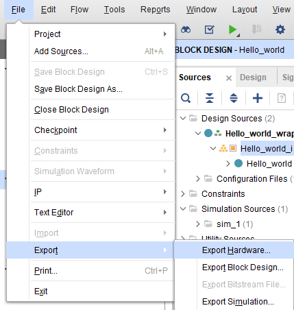
Now that implementation and generation of bitstream has been successfully completed, we need to export the hardware along with bitstream. Go to the “File” menu, select “Export->Export Hardware”.
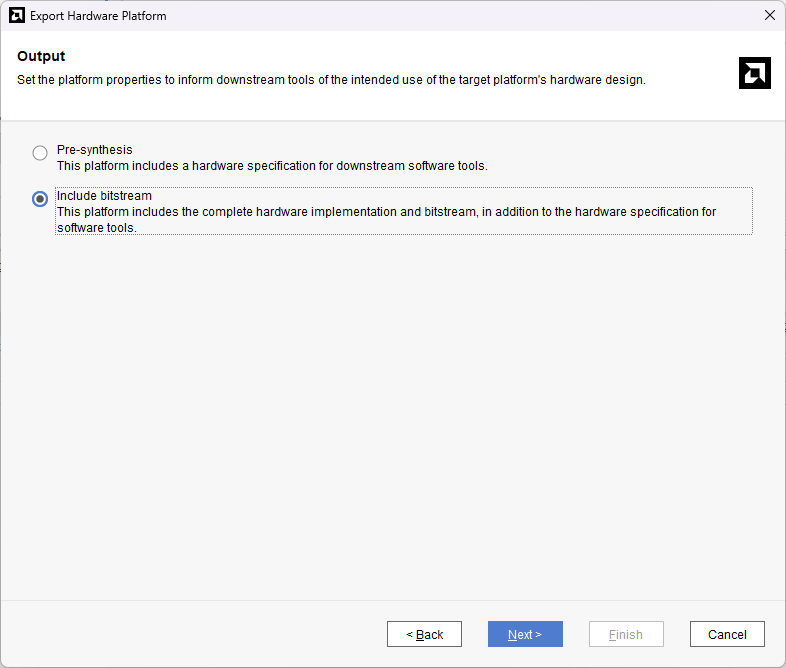
Select the “include bitstream” checkbox and click Next.
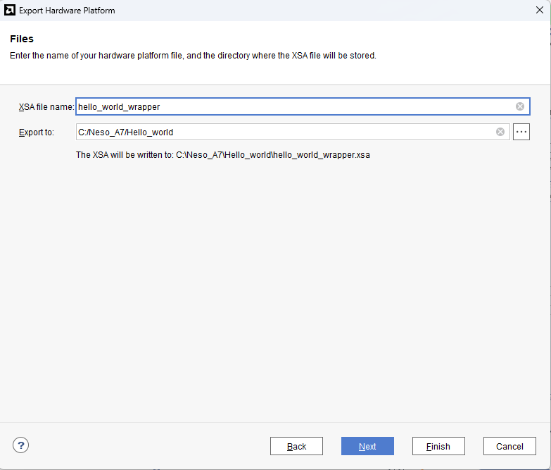
Provide the XSA file name and save it at a suitable location. Click Next and click Finish in the next dialog box.
Step 15:
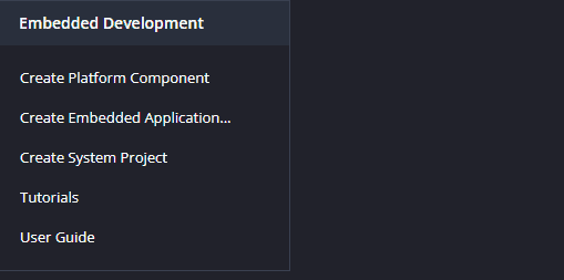
Launch Vitis IDE and create a new platform for the project, by selecting “Create Platform Component”, click “Next”, in the Flow tab select the XSA file saved using the step 15 and finally click “Next” and “Finish” respectively.
Step 16:
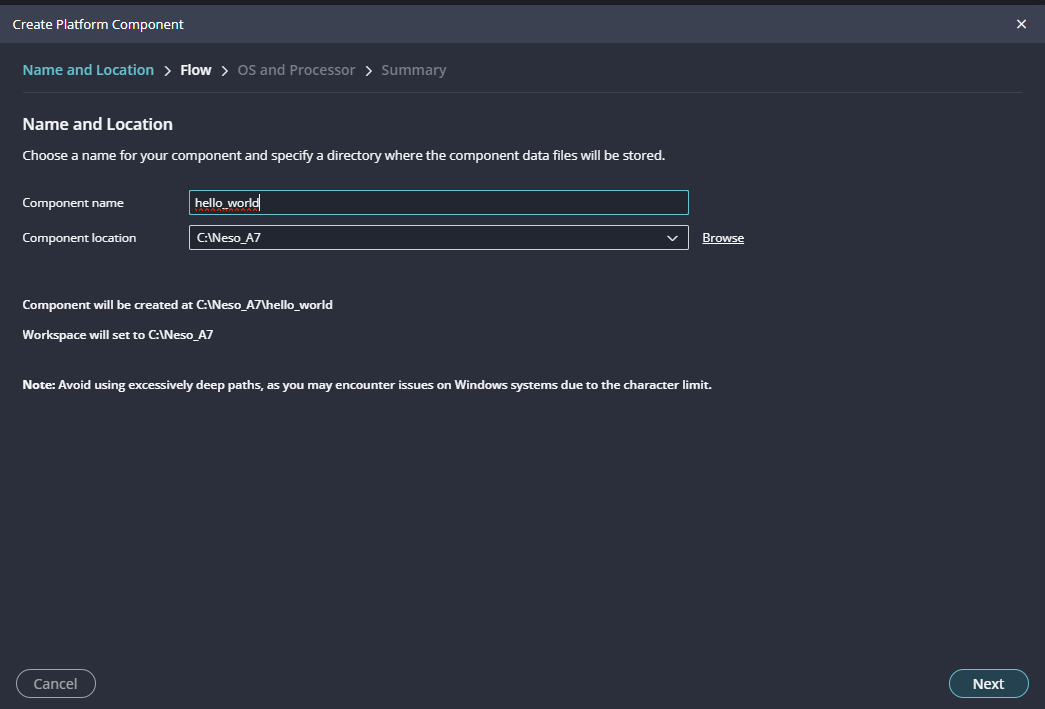
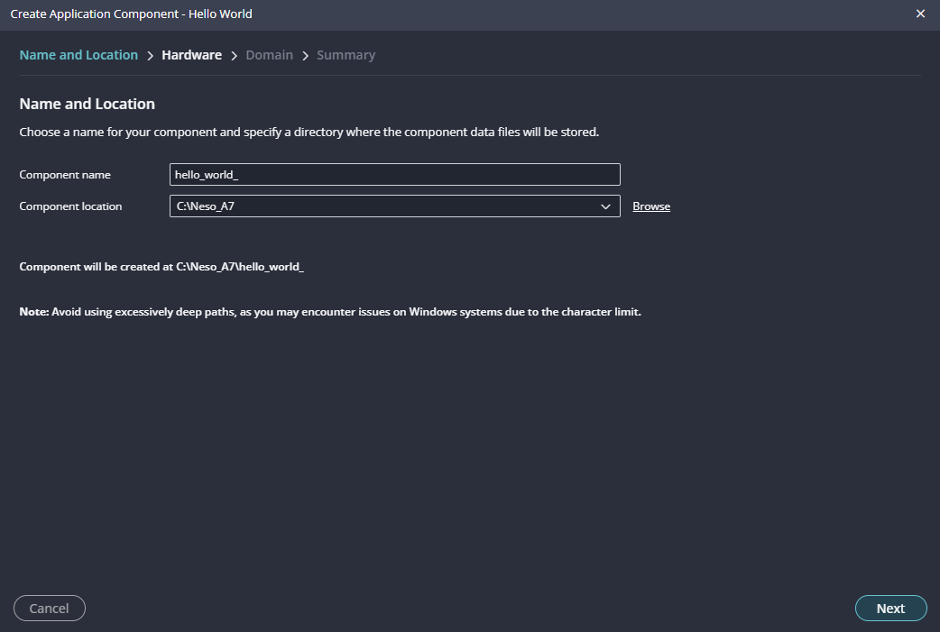
Give the component name and the platform location and click on “Next”.
Step 17:
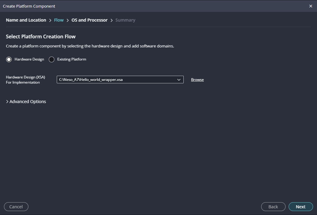
In the next tab browse the XSA file , select it , click on “Next”. In the next OS and Processor tab click “Next” and “Finish”.
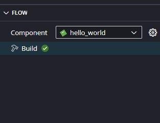
After successful creation of the platform, build the platform.
Step 18:
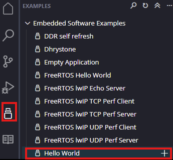
Next create the Hello world Application component by selecting the “Hello world” template from the “examples”.
In “Create Application Component” tab specify project name and location, click “Next”.
Select newly created Platform and click “Next”.
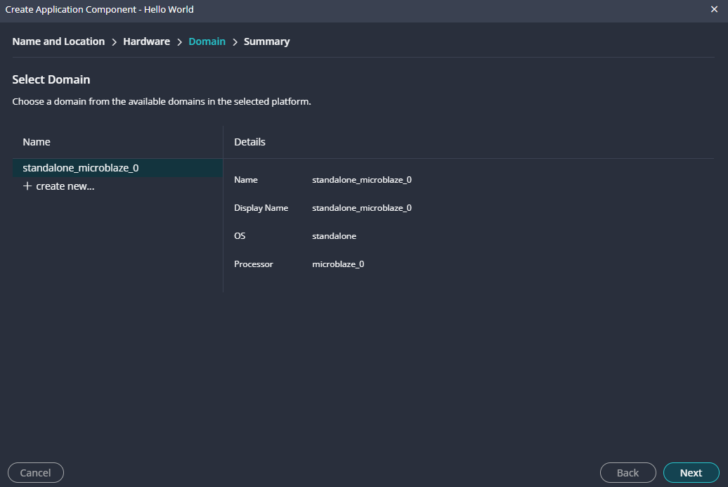
Select the domain as “Standalone_microblaze_0” and click “Next” and click on “Finish”.
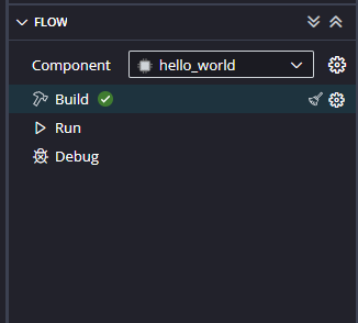
When the Hello world project is added successfully, build the project manually.
Step 19:
Once the build is completed successfully, power up Neso A7 FPGA Development Board using USB type C cable and connect the JTAG cable for programming the device.
Step 20:
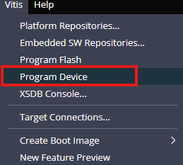
Program the FPGA on Neso A7 with a simple boot loop program by selecting the Program Device option from the Vitis menu.
Once the “Program Device” window opens give the path for .bit and .mmi files .
If the “BMM/MMI” File is not selected , manually browse and select the file .
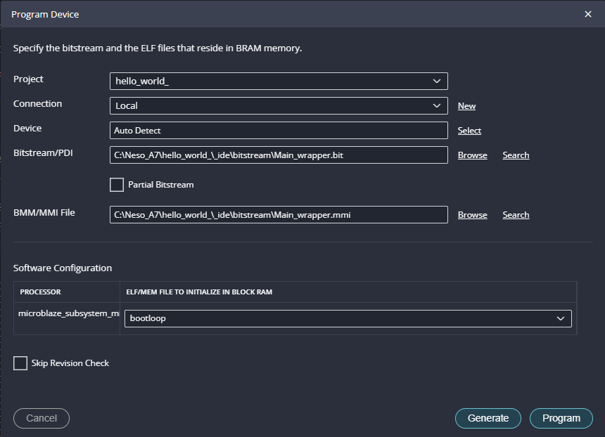
Once the files are selected click on “Program” .
Step 21:
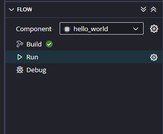
Meanwhile, open any serial terminal program (such as PuTTY, Teraterm etc) and open the port corresponding to Skoll Kintex 7 with a 9600 baud rate (the default baud rate given in UART IP). Program the board by selecting the “Run”.
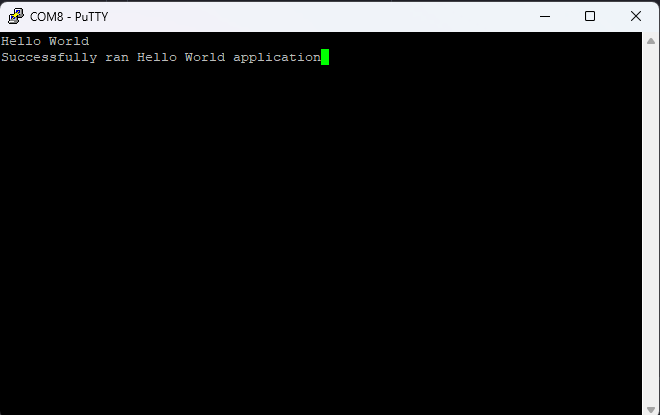
Step 22:
If everything went well, the application running on the board should print “Hello World” over the UART and should be displayed on the Serial Terminal application.