Introduction:
A Trusted Platform Module (TPM) is a dedicated microcontroller designed to secure hardware through integrated cryptographic keys. It plays a crucial role in establishing a hardware-based root of trust, helping ensure system integrity, data protection, and secure authentication. On the Aller AU-Plus FPGA module, the TPM IC enables robust security features such as secure boot, key storage, device identity, and data encryption, making it ideal for applications that demand high levels of trust and reliability. Whether you are working on embedded security, firmware protection, or secure communications, understanding and using the TPM is a foundational step toward building secure embedded systems.
Prerequisites:
Hardware:
- Aller AU-Plus FPGA Module
- Aller AU-Plus Carrier
- Xilinx Platform Cable USB
- USB type C cable
Software:
- Vivado Design Suite with Vitis version 2024.1
- Serial Terminal (PuTTY, Tera Term, etc.)
Let’s get Started
Step 1:
Download and install Vivado Board Support Package files for Aller AU-Plus from here.
Step 2:
Start Vivado Design Suite, and select “Create Project” from Quick Start section. The project wizard will pop up. Press “next” to proceed with creating the project.
Step 3:
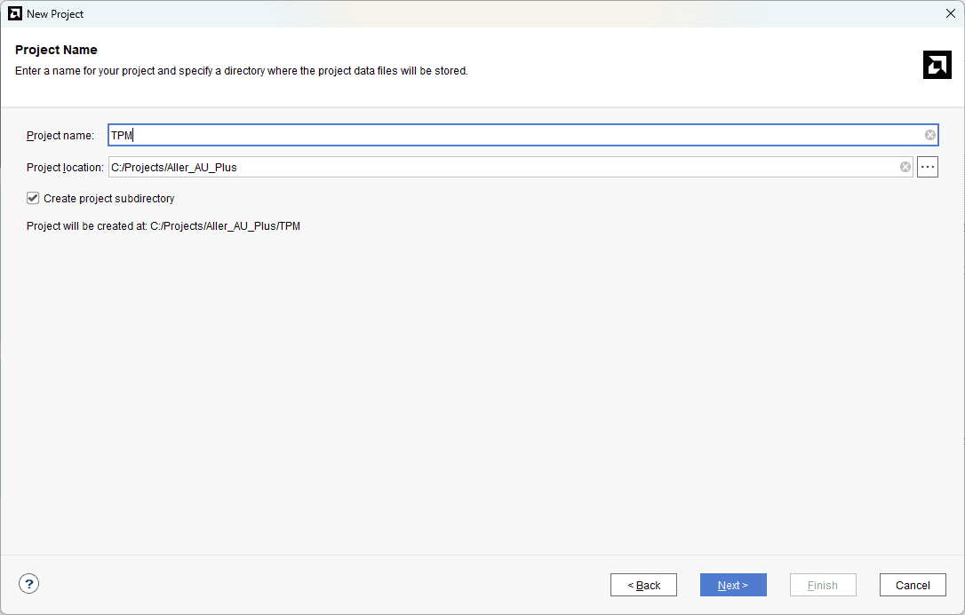
In the “Project Name” window, enter a name for the project and save it at a suitable location. Select the option “Create project subdirectory” to keep all the project files in a single folder and click “Next” without making any changes until you see the “Default Part” page.
Step 4:
In the “Default Part” window, select the “Boards” tab. Choose the Vendor as “numato.com”, filter the Name “Aller_AU_Plus” and select the board as shown below. If Aller_AU_Plus is not displayed in the Boards list, make sure that the board support files are installed correctly.
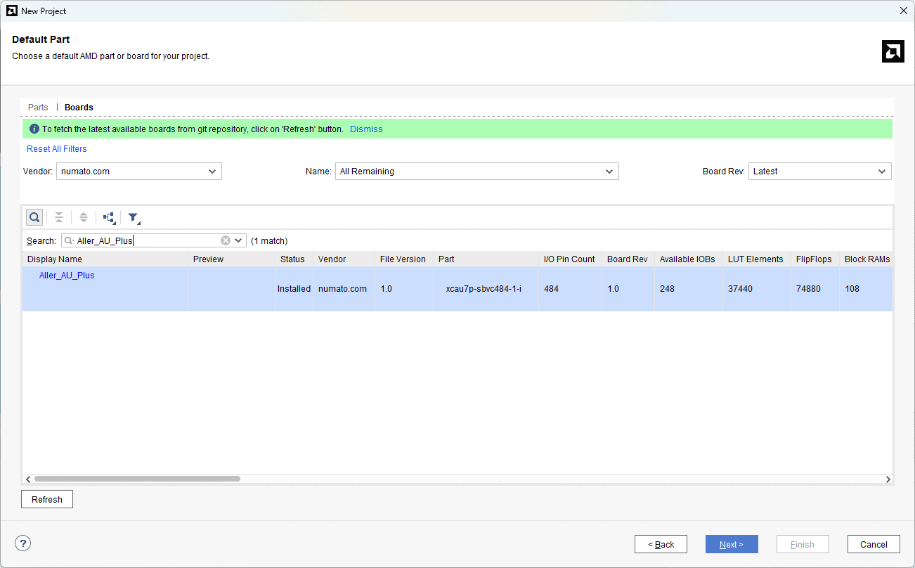
Click “Next” to continue. On the next page, click “Finish” to complete creating a new project. A new project will be created by Vivado with the selected settings.
Step 5:
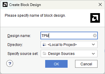
Under the “Flow Navigator” panel, click “Create Block Design” under the IP Integrator section. Enter a name for the block design and click “OK”.
An empty block design will be created.
Step 6:
Click the Board tab. The default peripherals available for the Aller _AU_Plus board will be displayed.
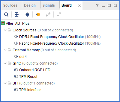
Drag and drop Fabric Fixed-Frequency clock Oscillator, TPM interface and TPM Reset into IPI Canvas.
Step 7:
Click Add IP, search for MicroBlaze, AXI Uartlite and Add it.
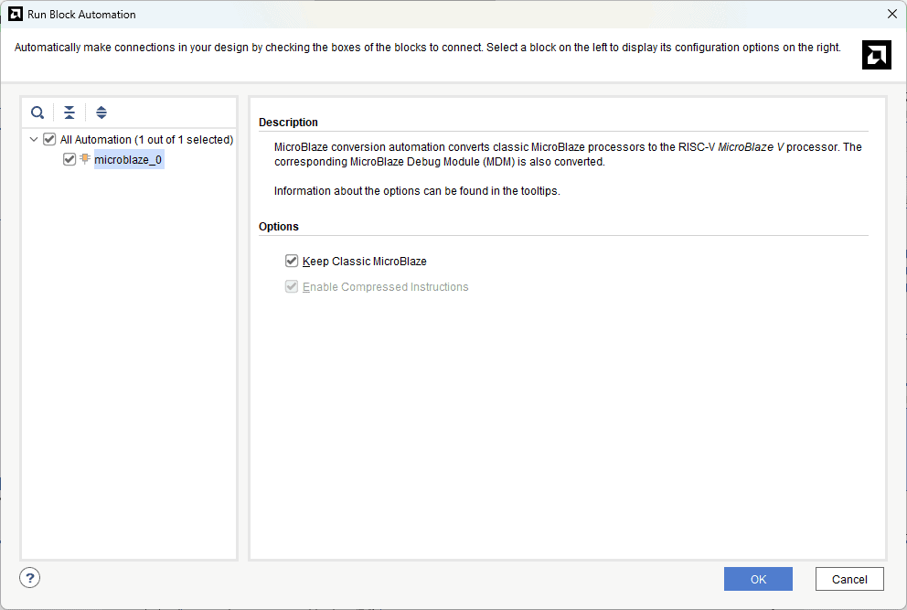
Click Run Block Automation with 64 KB of local memory and interrupt controller enabled.
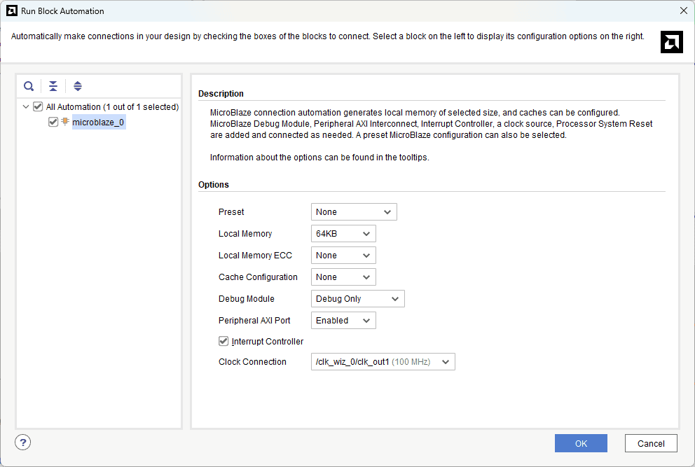
Click “OK” for Vivado to automatically configure the blocks for you. In Vivado 2024.1 after clicking on “OK” a window will appear, here you need to select “Keep Classic MicroBlaze” and then click OK to use Microblaze.
Step 8:
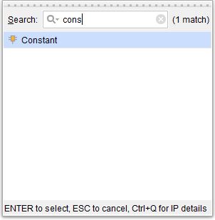
Press the “Add IP” icon and search for Constant block as shown in the image below. Drag and drop it to the Diagram window.
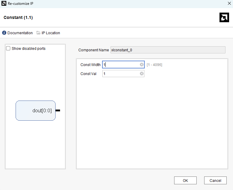
Double-click on the Constant block and confirm that its settings are as follows.
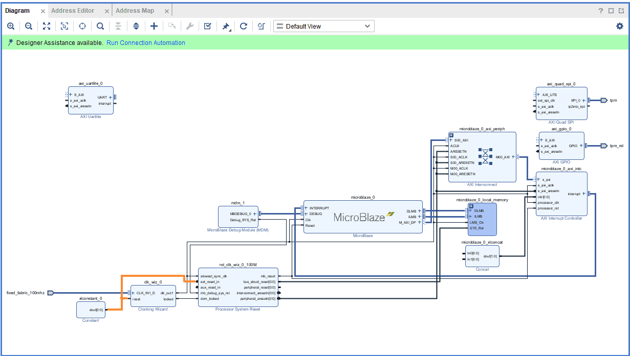
Now, connect the output of this block to reset of “Clocking Wizard” and ext_reset_in of the “Processor System Reset”. These connections are highlighted in orange in the following image.
Step 9:
Click “Run Connection Automation” and select the “All Automation” checkbox as shown in the image below. Click “OK”.
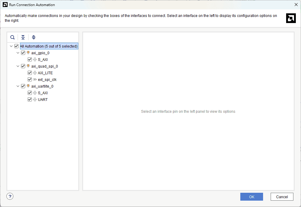
Vivado will now connect the blocks together to make a complete system.
Step 10:
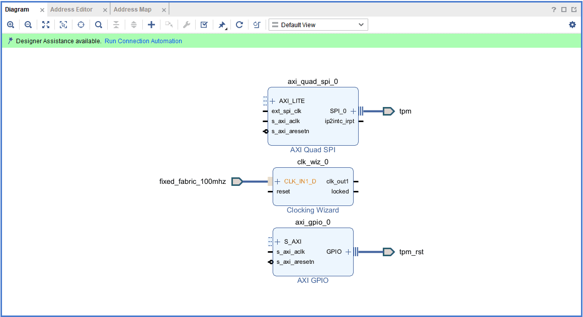
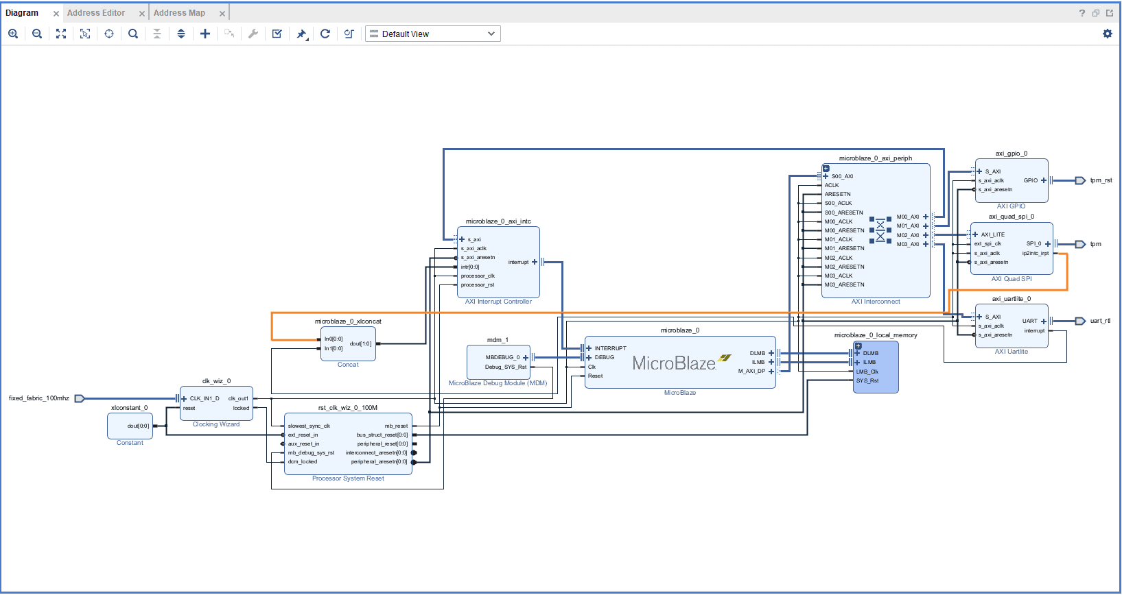
Connect the interrupts from axi_uartlite_0 and axi_quad_spi_0 to the Concat block as shown below (the order does not matter). Make sure that the final design looks similar to the image below.
Step 11:
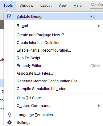
Select the “Validate Design” option from the Tools menu to ensure that the connections are correct and save the design.
Step 13:
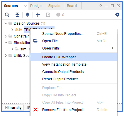
Right-click “TPM_i” in the “Sources” window, and select “Create HDL Wrapper” from the popup menu. Click “OK” on the window that appears to finish generating a wrapper.
Step 14:
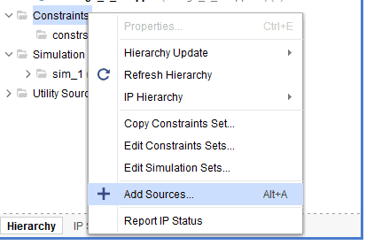
We have to add constraints for some ports in the design. Since we have BSP, most of the ports would be assigned from the BSP. We will have to manually assign for the rest of the ports. Right-click on “Constraints” in the Sources window, and select “Add Sources” as shown below.
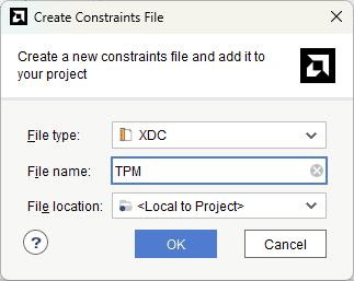
In the window that follows, select “Add or create constraints” and click “Next”. On the following page, select “Create File” and give an appropriate name to the constraints file, as shown below. Click “Finish”.
Step 15:
Copy the following constraints to the newly created constraints file and save it.
set_property PACKAGE_PIN W6 [get_ports uart_rtl_rxd]
set_property PACKAGE_PIN V6 [get_ports uart_rtl_txd]
set_property IOSTANDARD LVCMOS33 [get_ports uart_rtl_rxd]
set_property IOSTANDARD LVCMOS33 [get_ports uart_rtl_txd]
Step 16:
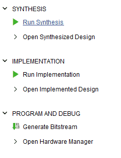
Click “Generate Bitstream” under the “Program And Debug” section to synthesize, implement and generate a bitstream.
Step 17:
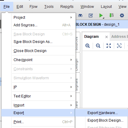
After generating the bitstream successfully, select Export -> Export Hardware from the File menu. Click Next.
Select the “include bitstream” checkbox and click Next.
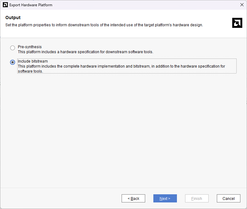
Provide the XSA file name and save it at a suitable location. Click Next and click Finish in the next dialog box.
Step 18:
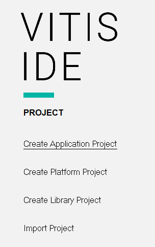
Launch Vitis IDE. In Vitis IDE window, select Create Application Project and click Next in the dialog box that appears.
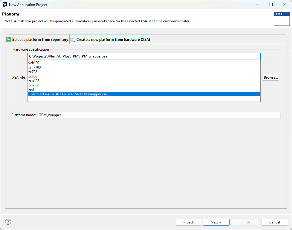
In the Platform window, select Create a new platform from hardware tab and import the XSA file which is already created (Provide XSA file location). Click Next.
Step 19:
In the Application Project Details window, give an appropriate name for the Vitis Project and click Next. Click Next in the Domain window.
Select the Hello World template from the list of available templates and click Finish.
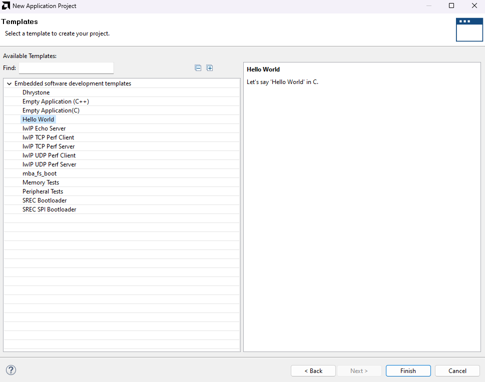
On the next page, select “Hello World” from the list of available templates and click “Finish”.
Step 20:
Replace the helloworld.c with the actual TPM code. Keep the rest of the files under src unchanged and build it.
Step 21:
Power up the Aller AU-Plus and connect the JTAG or USB-JTAG to the board for programming. Follow the steps mentioned under Programming Aller AU-Plus FPGA Module in the product user manual.
Step 22:
Open any serial terminal program (such as PuTTY, Teraterm etc) and open the port corresponding to Aller AU-Plus with a 9600 baud rate (the default baud rate given in UART IP).
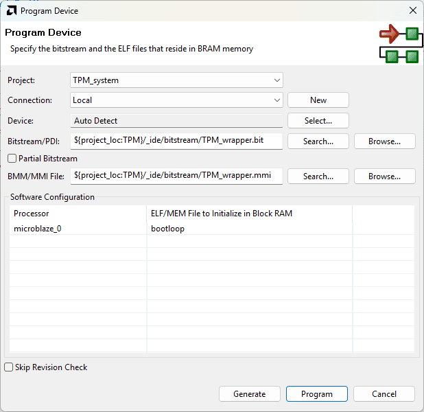
Step 23:
Program the FPGA on Aller with the generated bitstream and simple bootloop firmware by selecting the “Program Device” option from the “Vitis” menu.
Step 23:
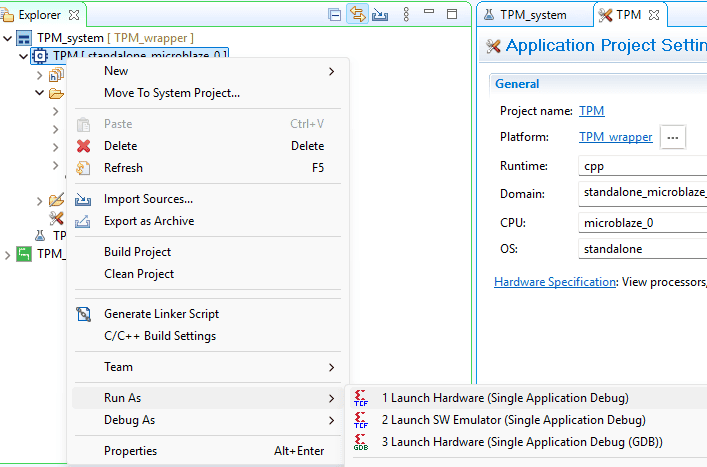
Right-click on the .elf file in the Project Explorer and select “Launch on Hardware” as shown below.
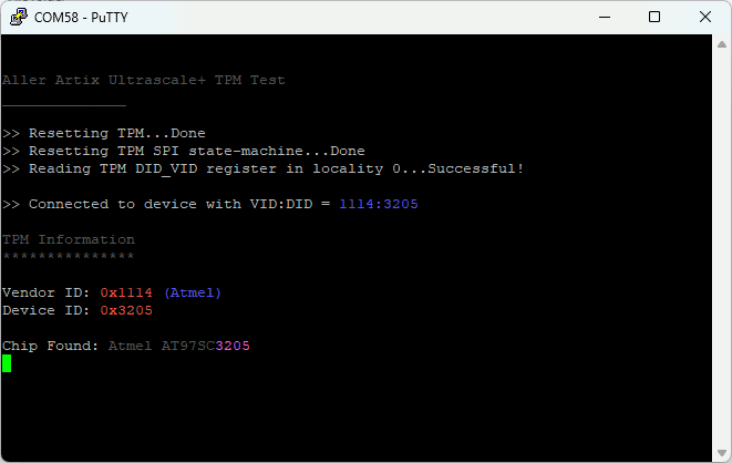
If everything went well, you will see the below output on the Serial Terminal application.