Ok, we have a module and tools ready now, let’s try to run a simulation on the module and see if it works as expected. To simulate the module, we need to give some input to the module, how do we do that? The answer is, that we need to create a test bench! The test bench will generate the necessary inputs for the module under analysis (Here “myModule”). A test bench is nothing but another Verilog module that generates some signals and feeds them to the module under test. During simulation, the test bench should be a “top module” (top-level module) with no I/O ports. But when it comes to implementation on real FPGA, the “top module” can have I/O ports and test benches won’t be the top modules there (we will talk about this in detail later). So here goes the test bench code.
module myModule_tb;
reg a,b;
wire y;

myModule uut(a,b,y);

initial begin
a = 0; b = 0;
#10
a = 0; b = 1;
#10
a = 1; b = 0;
#10
a = 1; b = 1;
#10
$finish();
end

endmodule
Let me break this down for you.
The test bench is just another module, with no I/O ports as I mentioned earlier. I have created a wire named “y” and reg named “a” and “b”. The wire “y” is connected to the output port (port B) of myModule. The result should appear on the wire “y” in the simulation.
The statement “myModule uut(a,b,y)” creates an instance of the module “myModule” with the name “myModule”. You can create as many instances as you want from a module. This line instantiates the module under test (myModule) with inputs a and b, and output y. The instance name is uut.
The next block is an initial block. As its name suggests, this block will be executed only once. So anything that we need to initialize should go here. Initial block also is usually used only in test benches. Initial blocks are rarely used in synthesizable code, instead, reset logic is created if initialization is required.
In this initial block
- Inputs a and b are set to 0.
- After a delay of 10 time units (#10), inputs a and b are updated to simulate different input combinations.
- This sequence tests all possible input combinations (00, 01, 10, 11) of the module under test.
- After the final input combination, the simulation is terminated using the $finish system task.
“endmodule” concludes the definition of the testbench module.
Now it is time to run the simulation. Follow the steps below to simulate Xilinx Vivado Design Suite(Images are based on Xilinx Vivado Design Suite 2023.2.1).
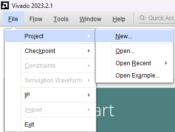
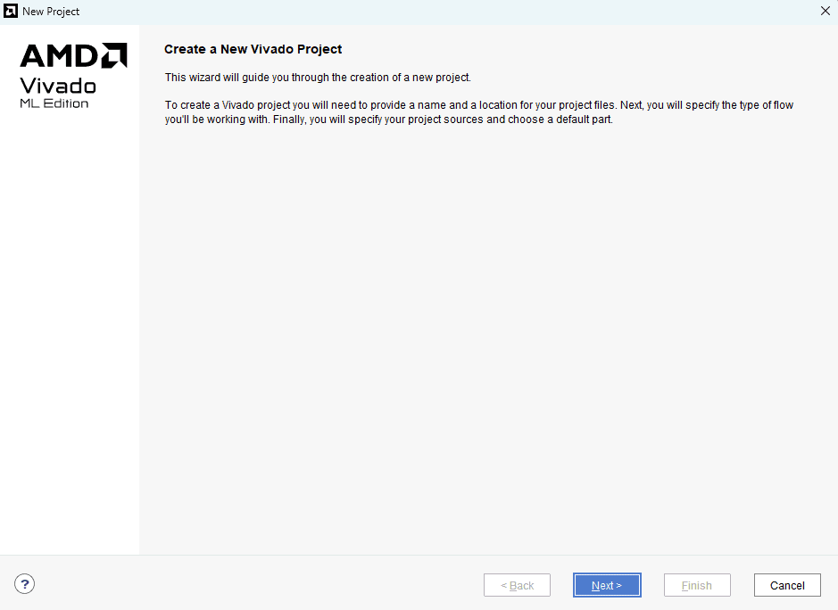
Step 1 : Launch Vivado Design Suite, go to “File->Project->New” to create a new project. The “New project” wizard will pop up. Click “Next” to continue
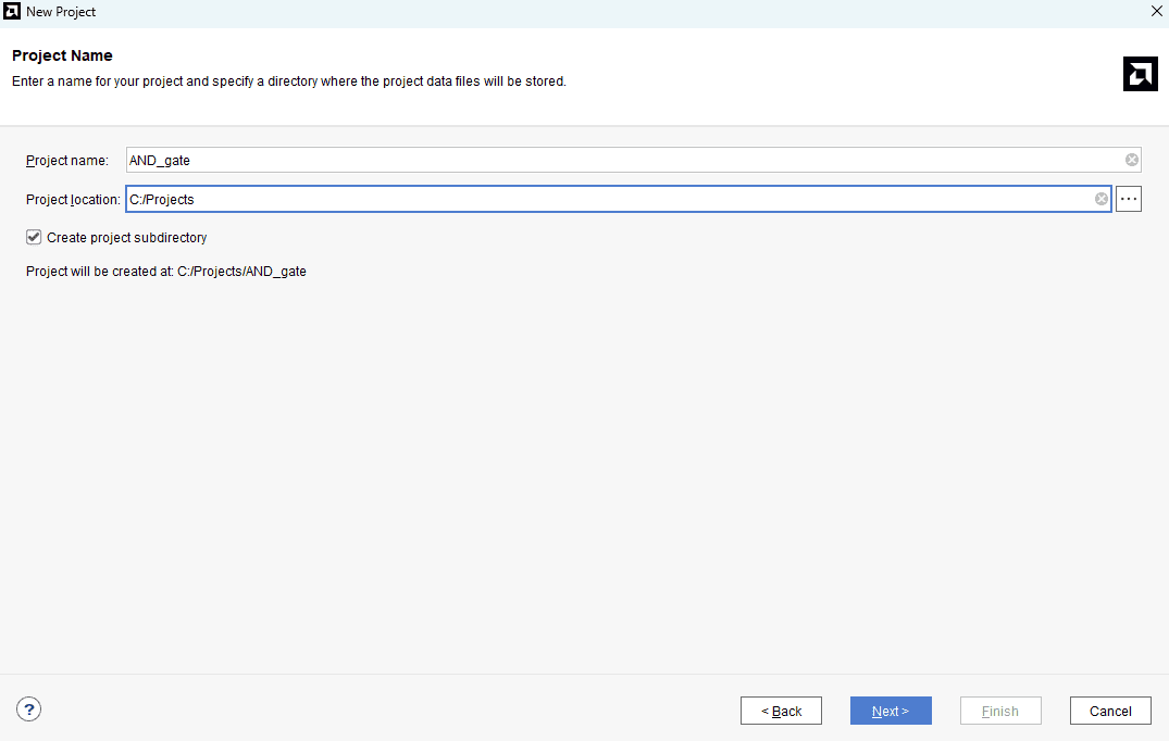
Step 2 : Name your project select a directory to save the project and click “Next” (refer to the picture below).
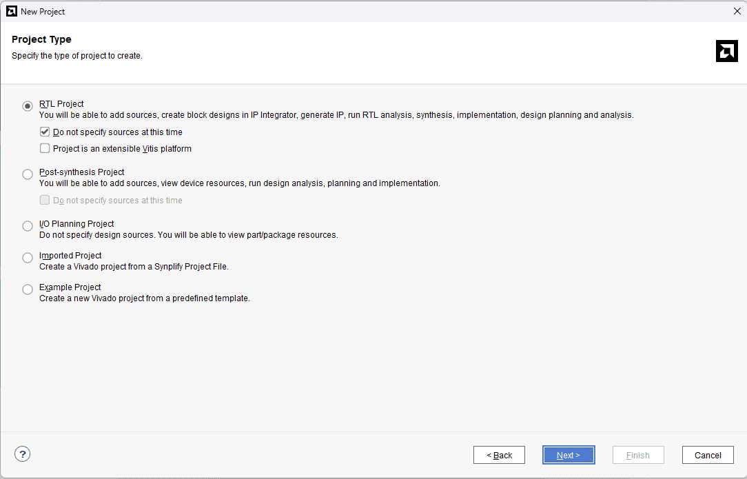
Step 3 :In the “Project Type” window, select “RTL Project” and check the “Do not specify sources at this time”. Click “Next”.
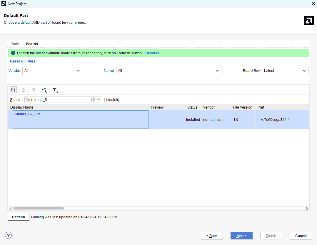
Step 4 :In the “Default Part” tab, select “Mimas_S7_lite” from the “Boards” section. If Mimas_S7_lite is not listed, make sure board support files are installed correctly. Click “Next” to proceed.
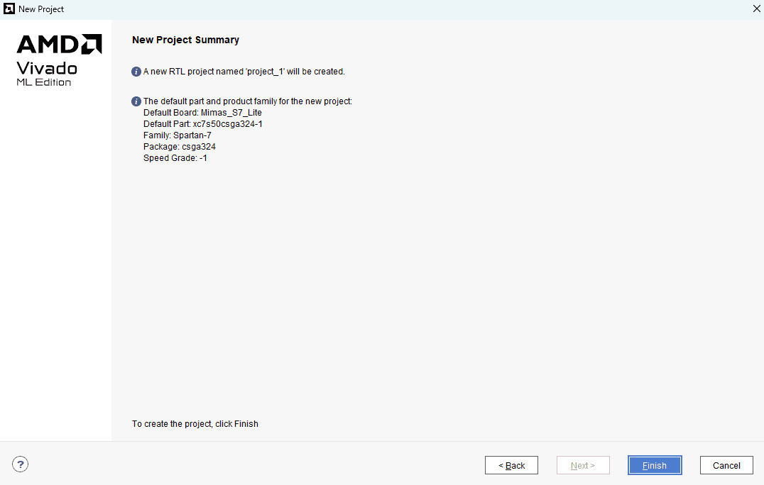
Step 5 :Click “Finish” to create a new project.
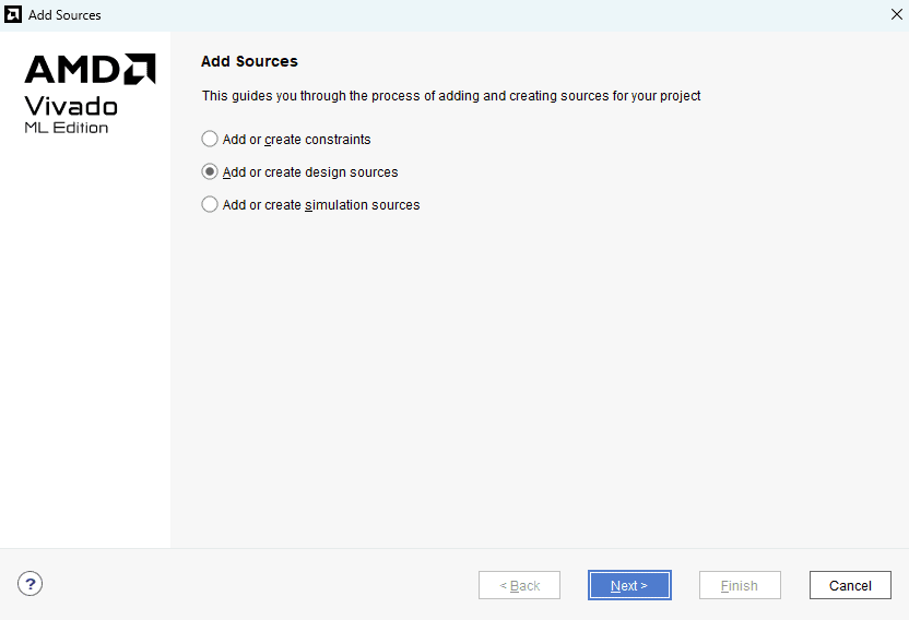
Step 6 :To design a AND Gate, we have to add sources to the project. To do this, select “Add Sources” under the “Flow Navigator” -> “PROJECT MANAGER” section. Now select “Add or create design sources” and click “Next”.
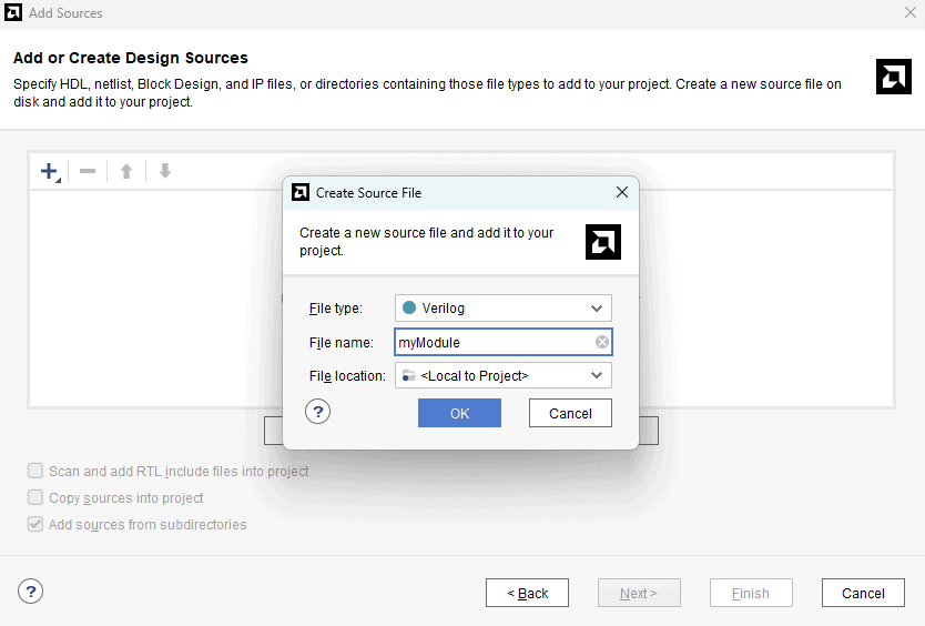
Step 7:Now, select “Create File”. The “Create Source File” window will open, select the “File type” as “Verilog” and give the file name as in the image below. Click “OK” and then click “Finish”.
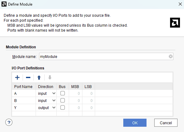
Step 8 :The “Define Module” window will open. Now, we have to add the ports required for our project. For our AND Gate module, we will need 3 ports. “A” and “B” as the input port and “Y” as the output port. To add these ports to our project, in the “Define Module” window click on the “+” button to add ports and name the ports and change the direction of the port appropriately. Click “OK”. (refer the image below)
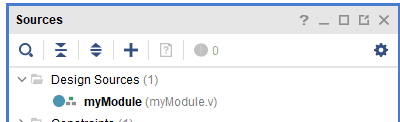
Step 9 :The source file myModule.v will be available under “Sources->Design Sources”. Double click on the source file to open it.
Step 10 : Now replace the auto-generated module template (or the contents of the whole file) with the code below and save the Verilog source file.
module myModule(a,b,y);
input wire a;
input wire b;
output wire y;

assign y = a & b;

endmodule
Now its time to simulate the code. To run the simulation, we will have to add the simulation sources. To do this, follow the steps below.
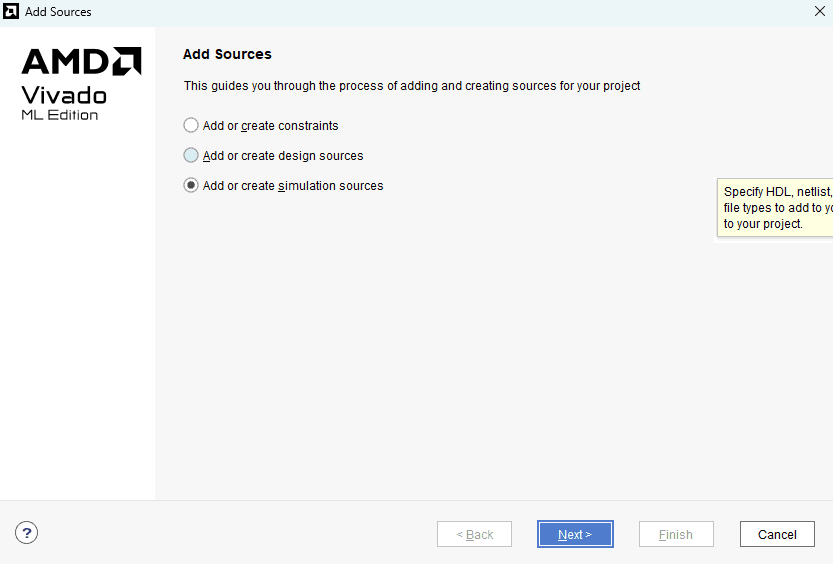
Step 11 : Again, select “Add Sources” under the “Flow Navigator” -> “PROJECT MANAGER” section. This time select “Add or create simulation sources” and click “Next”.
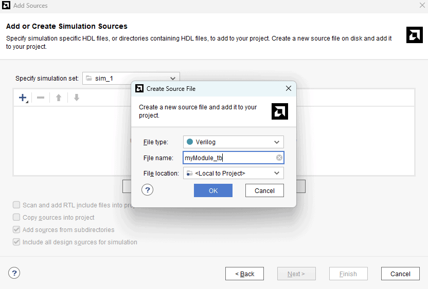
Step 12 : Select “Create File”, give the name for the test bench as “myModule_tb” and choose “File type” as “Verilog” as in the image below. Click “OK” then “Finish”.
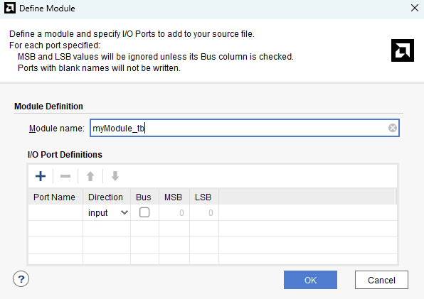
A test bench does not need any Inputs and Outputs, so just click “OK” and click “Yes” in the corresponding window that appears.
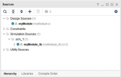
Now the test bench will be created under “Sources -> Simulation Sources”.
Replace the auto-generated module template with the following code and save it.
 module myModule_tb;
 reg a,b;
 wire y;
 myModule uut(a,b,y);
 initial begin
 a = 0; b = 0;
 #10
 a = 0; b = 1;
 #10
 a = 1; b = 0;
 #10
 a = 1; b = 1;
 #10
 $finish();
 end
 endmodule
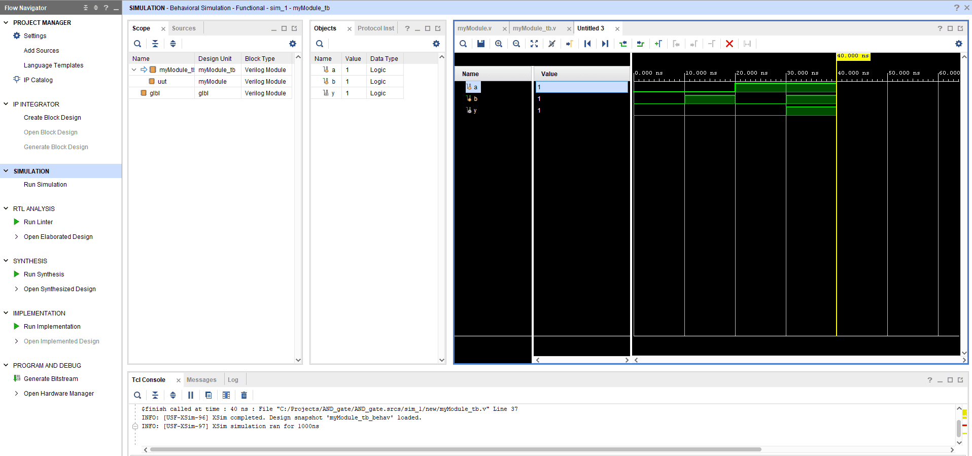
Step 13 : Now click on “Run Simulation” –> “Run Behavioral Simulation” under the “Flow Navigator” –> “SIMULATION” panel.
Step 14 : Now the built-in simulator will start and you will be presented with a simulation waveform like the one below (Sometimes you may have to zoom in/out a little bit to see the waveform correctly).
Inspect the waveform and make sure that our Verilog module is working as expected. As you can see in the image below, the output is the high(1) only when both the inputs are high(1). This is exactly what we expect from an AND gate.
In part 4 of this tutorial, we will implement this module on a real hardware.
Back to part 2 Continue to part 4