What sets Verilog apart from traditional programming languages like C or C++ is its parallel nature. In the world of Verilog, actions don’t always happen one after the other in a sequential manner. Instead, they occur simultaneously. Consider a traffic light controller, for example. In Verilog, you can model each aspect of its operation – the changing of lights, the detection of vehicles, and the synchronization of traffic flow – all happening concurrently. This parallelism mirrors the real-time operation of the controller, where different signals are processed simultaneously to manage traffic efficiently. Similarly, in Verilog, you can design complex digital circuits composed of interconnected modules, each performing its own function independently. These modules operate in parallel, exchanging information and influencing each other’s behavior without waiting for sequential instructions. This parallelism is deeply ingrained in the fabric of Verilog, reflecting the inherent parallelism of digital hardware. Unlike the linear execution of code in traditional software, Verilog embraces the simultaneous execution of tasks, harnessing the power of parallel processing to design and simulate intricate digital systems.
Verilog Modules
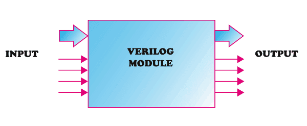
Verilog modules are fundamental building blocks in Verilog HDL (Hardware Description Language) used to design digital circuits. Think of them as individual components or functional units within a larger digital system. These modules encapsulate specific functionality and can range from simple gates like AND or NOT gates to complex processors or controllers. In essence, Verilog modules define the behavior and structure of a particular component in the digital circuit. They have inputs and outputs, which represent the signals entering and leaving the module, respectively. These inputs and outputs are connected to other modules or components within the overall design. Verilog modules allow for modularity and abstraction in digital design. By breaking down a complex system into smaller, more manageable modules, designers can focus on implementing specific functionality without worrying about the details of the entire system. This modular approach also enables easier debugging, testing, and reuse of components across different projects.
Furthermore, Verilog modules can be instantiated multiple times within a design, allowing for the creation of hierarchical structures. This hierarchical organization helps in organizing and managing large-scale designs effectively.
Enough talk, we didn’t even write a “Hello World” program yet. So how do we get our hands dirty with Verilog? Let us design an AND gate in Verilog, simulate it and test it in a real hardware. It’s a simple gate that only gives an output of 1 (or “high”) when both of its inputs are also 1. Otherwise, it gives an output of 0 (or “low”). Below table summarize the behavior of AND gate as a truth table.
| INPUT A | INPUT B | OUTPUT Y |
|---|---|---|
| 0 | 0 | 0 |
| 0 | 1 | 0 |
| 1 | 0 | 0 |
| 1 | 1 | 1 |
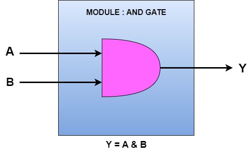
AND gate can be considered as a module with two inputs and one output, where the internal behavior follows the logic of the Boolean expression Y = A & B. See the graphical representation of the AND gate module below:
Let us see how we would represent this in Verilog.
module myModule(a,b,y);
input wire a;
input wire b;
output wire y;
assign y = a & b;
endmodule
Very simple isn’t it? let us go through each and every line and try to understand what is going on in this bit of code.
The name of the module is “myModule” and is declared using the “module” keyword. The keyword module in Verilog defines our module (called myModule) and assign three ports to it. Everything that goes into this module is placed in between “module” and “endmodule” keywords. myModule has three ports. The ports’ size or direction is not known yet.
In the two lines below, port A and port B are declared as input and port Y as output respectively. I’m sure you are curious about what the keyword “wire” is doing there! Well, in Verilog there are two fundamental data types, ‘wire’ and ‘reg’. There are many other data types like int, real etc… But ‘wire’ and ‘reg’ plays very important roles in Verilog, that without learning them we cannot progress much.
As I mentioned before, knowing a little digital electronics will come handy here. ‘wire’ is just like a physical wire that we use to connect two different things electrically. If a potential is applied at one end of a copper wire, it will show up on the other end of the wire as long as you keep applying the potential. As soon as you remove the input, the potential is gone. This is true for a ‘wire’ data type in Verilog as well. A wire will have a particular logic state as long as it is driven by some other entity. If nobody is driving the wire, it will be in an unknown state. In Verilog, ‘wire’ can be used to connect things within a module or between two modules.
On the other hand, ‘reg’ can store a logic state and maintain it until someone changes it (think about a register in a microcontroller). This is similar to a flip-flop. If you put flip-flop in one state, it will remain in that state until somebody changes it.
So you can use wire as input or output for a module and ‘reg’ can be used as an output of a module. When wire is used as output, there should be a ‘reg’ that drives the wire from within the module so that ‘wire’ will have some meaningful information on it. If ‘reg’ is used as output, no other mechanism is necessary since it can hold data on its own.
Then why “myModule” has both input and output declared as wires? Good question, the answer is, because the module represents an AND gate. Gates never store any state. Gates are purely combinational; i.e. its output always depends on the current input. If there is some logic state applied to its input then there will be a corresponding output (Y = A & B in this case). If no logic state is applied to the input it is considered as unknown state and the output state will also be unknown. And this also implies that to have any useful output from this module, some other entity should be driving its input from somewhere else (keep this in mind, we will touch this subject later when talking about test bench).
One more important thing about the above code is the keyword “assign”. The assign keyword is used to create combinational circuits. Whatever written on the right side of equal sign in the statement will be evaluated and the result will be assigned to the entity on the left side and this happens asynchronously. As soon as any changes happen on the right side, the result will be reflected on the left side. If you find it difficult to understand this, you may want to read a little about combinational digital circuits.
Now that we have a piece of code, we may want to simulate the code to see if it is working as expected. Simulation, in a broad sense, is the process of giving some known input and generating the corresponding output. The output is expected to be dependent on both the input and the behavior of the module under test. When the output is verified against expected output, it is called verification. There are many tools available for simulation and verification. Here we will be using the inbuilt simulator (part of Xilinx Vivado Design Suite) for simulation and waveform inspection.
Back to part 1 Continue to part 3
