Introduction
We’ll walk you through the steps of interfacing a seven-segment display with the Mimas AU-Plus using Vivado IP Integrator and creating a counter that goes all the way to 1000.
Prerequisites:
Hardware:
- Mimas AU-Plus FPGA Development Board.
- AMD Platform Cable USB II JTAG debugger.
- USB type C cable.
Software:
- Vivado Design Suite 2025.1
Creating Microblaze based Hardware Platform for Mimas AU Plus
The following steps will walk you through the process of creating a new project with Vivado and building a hardware platform . Numato Lab’s Mimas AU-Plus FPGA Development Board is used in this example, but any compatible FPGA platform can be used with minor changes to the steps. Screenshots are added wherever possible to make the process easier for the reader.
Step 1:
Download and install Vivado Board Support Package files for Mimas AU-Plus from here.
Step 2:
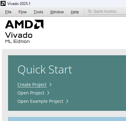
Start Vivado Design Suite, and select “Create Project” from Quick Start section. The project wizard will pop up. Press next to proceed with creating the project.
Step 3:
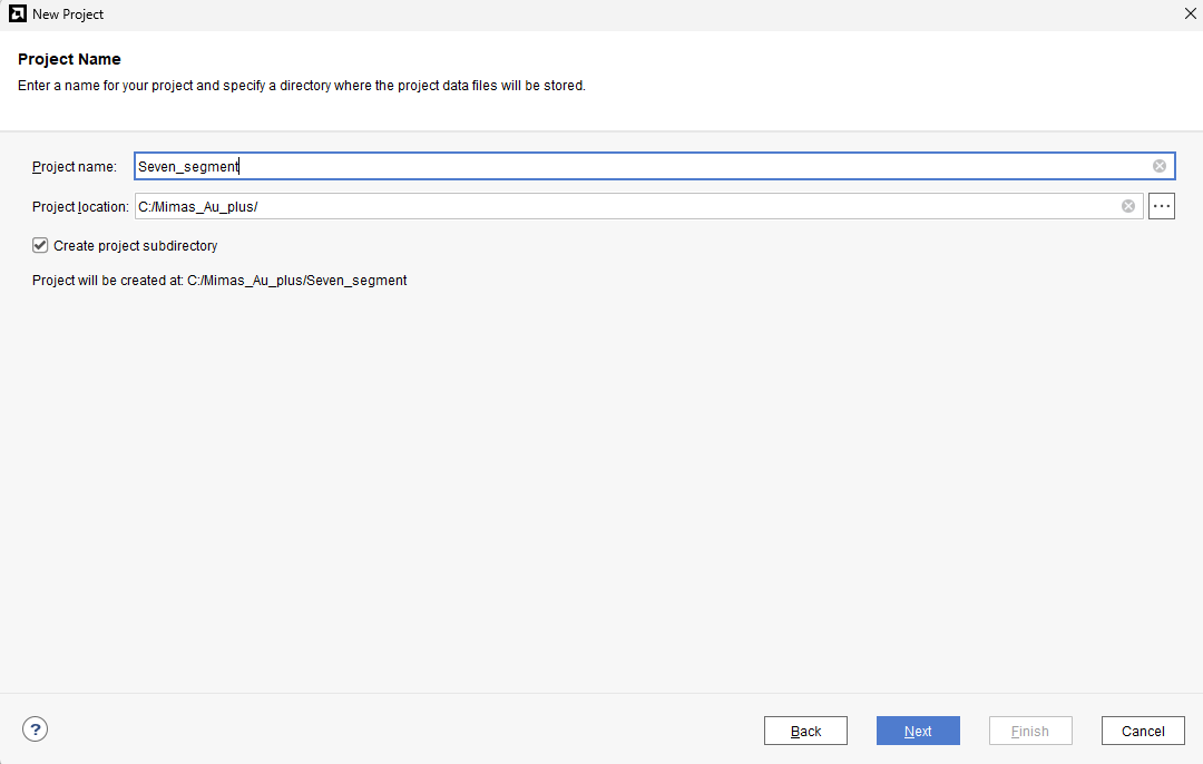
Enter a name for the project and save it at a suitable location. Check the option “Create project subdirectory”. Click Next to continue.
Step 4:
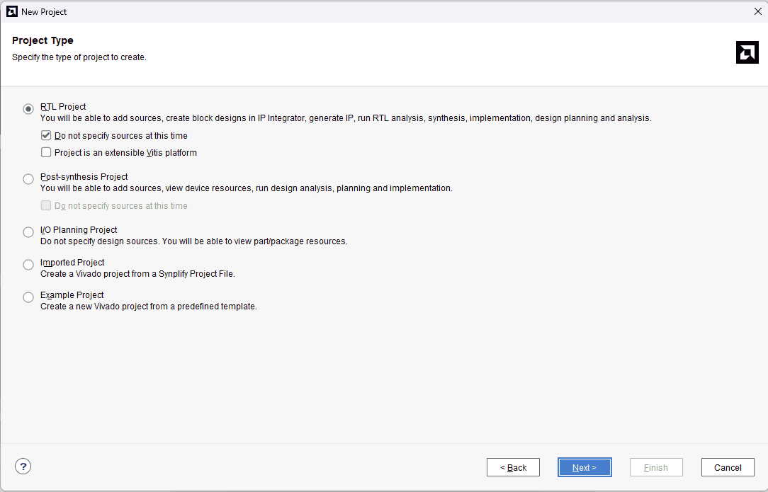
In the Project Type window, select RTL Project and check the option “Do not specify sources at this time”. Click Next.
Step 5:
In the Default Part window, select “Mimas_AU_Plus_dev_VA0.0” from the Boards option. If not listed, make sure board support files are installed correctly. Click Next to continue.
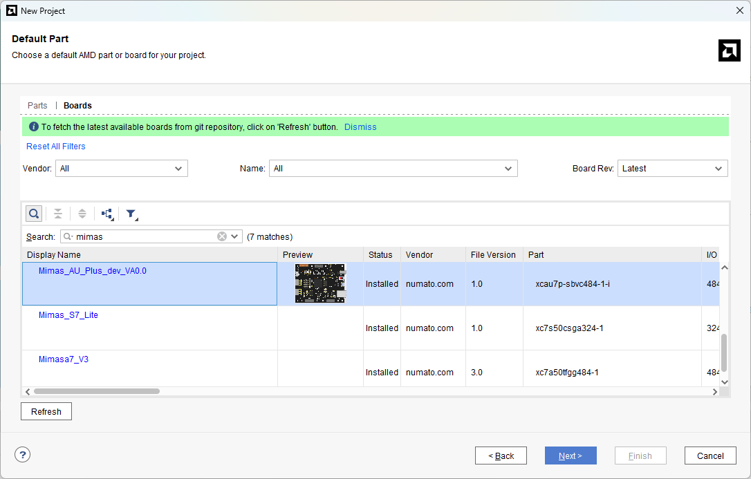
Click Finish to complete creating a new project. A new project will be created by Vivado with the selected settings.
Step 5:
In the “Sources” tab, right-click on the “Design Sources” and select “Add Sources”. It will open a new “Add Sources” window.
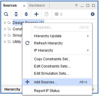
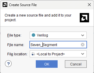
Create a new Verilog file by giving any convenient name to it.
Add the following Verilog Code to the newly created verilog file:
module Seven_segment_LED_Display_Controller(
    input wire clk_p,           // 100 MHz differential clock positive input (from board)
    input wire clk_n,           // 100 Mhz clock source on Basys 3 FPGA (or Mimas AU Plus)
    input wire reset,           // reset (external, active high)
    output reg [3:0] DIG,       // anode signals of the 7-segment LED display
    output reg [7:0] LED_out    // cathode patterns of the 7-segment LED display
);

    reg [26:0] one_second_counter;  // Counter for generating 1 second clock enable
    wire one_second_enable;         // One second enable pulse for counting numbers

    reg [15:0] displayed_number;    // Counting number to be displayed (up to 1000)
    reg [3:0] LED_BCD;              // BCD value for the current digit to be displayed

    reg [19:0] refresh_counter;     // 20-bit for creating 10.5ms refresh period or 380Hz refresh rate
                                    // The first 2 MSB bits for creating 4 LED-activating signals with 2.6ms digit period
    wire [1:0] LED_activating_counter; // Used to select which of the 4 digits is active


    wire clk_100mhz;        // Clean 100MHz clock output from MMCM
    wire clk_wiz_locked;    // MMCM lock status (active high when locked)

    // Basic Power-on Reset (POR) counter - this just counts down

    reg [9:0] por_counter = 1023;
    always @ (posedge clk_p) begin
        if (por_counter) begin
            por_counter <= por_counter - 1 ;
        end
    end

    clk_wiz_0 clk_wiz_inst (
        .clk_in1_p(clk_p),      // Connect to differential P input
        .clk_in1_n(clk_n),      // Connect to differential N input
        .clk_out1 (clk_100mhz), // Connect MMCM output to internal clock
        .reset   (reset),       // Connect board reset button to MMCM reset (ensure debounced/synchronized in XDC)
        .locked  (clk_wiz_locked) // Output MMCM locked status
    );

    // Logic to generate a 1-second enable pulse
    always @(posedge clk_100mhz or posedge reset) begin
        if(reset==1) begin // Active high reset
            one_second_counter <= 0;
        end else begin
            // Count up to 99,999,999 (0 to 99,999,999 is 100,000,000 cycles for 1 second at 100MHz)
            if(one_second_counter == 99999999) begin
                one_second_counter <= 0; // Reset counter for next second
            end else begin
                one_second_counter <= one_second_counter + 1;
            end
        end
    end
    assign one_second_enable = (one_second_counter == 99999999) ? 1 : 0; // Pulse high for one clock cycle per second


    always @(posedge clk_100mhz or posedge reset) begin
        if(reset==1) begin
            displayed_number <= 16'd0; // Reset count to 0
        end else if(one_second_enable==1) begin // Only increment when one second has passed
            if(displayed_number < 16'd1000) begin // Only increment if current number is less than 1000
                displayed_number <= displayed_number + 16'd1; // Increment count
            end
            // Else (if displayed_number is 1000 or greater), it will stay at its current value (1000).
        end
    end

    // Refresh counter for multiplexing (runs continuously)
    always @(posedge clk_100mhz or posedge reset) begin
        if(reset==1) begin
            refresh_counter <= 0;
        end else begin
            refresh_counter <= refresh_counter + 1;
        end
    end

    // Use the two MSBs of refresh_counter to select which digit to activate
    assign LED_activating_counter = refresh_counter[19:18];

    // Decoder to generate anode signals and select the BCD digit from displayed_number
    // Anode activating signals for 4 LEDs, digit period of ~2.6ms
    always @(*) begin
        case(LED_activating_counter)
            2'b00: begin // Activates LED1 (most significant digit)
                DIG = 4'b0111; // Example: Activate DIG[0] (active low)
                LED_BCD = displayed_number / 1000; // Thousands digit
            end
            2'b01: begin // Activates LED2
                DIG = 4'b1011; // Example: Activate DIG[1] (active low)
                LED_BCD = (displayed_number % 1000) / 100; // Hundreds digit
            end
            2'b10: begin // Activates LED3
                DIG = 4'b1101; // Example: Activate DIG[2] (active low)
                LED_BCD = ((displayed_number % 1000) % 100) / 10; // Tens digit
            end
            2'b11: begin // Activates LED4 (least significant digit)
                DIG = 4'b1110; // Example: Activate DIG[3] (active low)
                LED_BCD = ((displayed_number % 1000) % 100) % 10; // Ones digit
            end
            default: begin // Should not happen with 2-bit counter
                DIG = 4'b1111; // All digits off
                LED_BCD = 4'b0000; // Display 0 (or blank)
            end
        endcase
    end

    // Cathode patterns of the 7-segment LED display (assuming common anode, active low segments)

    always @(*) begin
        case(LED_BCD)
            4'b0000: LED_out = 8'b00000001; // Displays 0 (dp off)
            4'b0001: LED_out = 8'b11010111; // Displays 1 (dp off)
            4'b0010: LED_out = 8'b00100010; // Displays 2 (dp off)
            4'b0011: LED_out = 8'b10000010; // Displays 3 (dp off)
            4'b0100: LED_out = 8'b11000100; // Displays 4 (dp off)
            4'b0101: LED_out = 8'b10001000; // Displays 5 (dp off)
            4'b0110: LED_out = 8'b00001000; // Displays 6 (dp off)
            4'b0111: LED_out = 8'b11000011; // Displays 7 (dp off)
            4'b1000: LED_out = 8'b00000000; // Displays 8 (dp off)
            4'b1001: LED_out = 8'b11000000; // Displays 9 (dp off)
            default: LED_out = 8'b11111111; // All segments off (dp off) for invalid BCD
        endcase
    end

endmodule
This Verilog module implements a 7-segment LED display controller that counts from 0 to 1000, incrementing once per second. It utilizes a clock management unit to provide a stable 100MHz clock and a power-on reset for initialization. A dedicated counter tracks 100 million clock cycles to generate a precise one-second enable pulse, which then triggers the increment of the displayed_number. The module employs display multiplexing, rapidly cycling through four 7-segment digits by activating their anodes sequentially, while simultaneously calculating and presenting the correct BCD value for each digit’s segments (cathodes). This high-speed multiplexing creates the illusion of a continuously lit four-digit display showing the current count.
  always @(*) begin
        case(LED_BCD)
            4'b0000: LED_out = 8'b00000001; // Displays 0 (dp off)
            4'b0001: LED_out = 8'b11010111; // Displays 1 (dp off)
            4'b0010: LED_out = 8'b00100010; // Displays 2 (dp off)
            4'b0011: LED_out = 8'b10000010; // Displays 3 (dp off)
            4'b0100: LED_out = 8'b11000100; // Displays 4 (dp off)
            4'b0101: LED_out = 8'b10001000; // Displays 5 (dp off)
            4'b0110: LED_out = 8'b00001000; // Displays 6 (dp off)
            4'b0111: LED_out = 8'b11000011; // Displays 7 (dp off)
            4'b1000: LED_out = 8'b00000000; // Displays 8 (dp off)
            4'b1001: LED_out = 8'b11000000; // Displays 9 (dp off)
            default: LED_out = 8'b11111111; // All segments off (dp off) for invalid BCD
        endcase
    end

endmodule
This block of Verilog code implements a BCD (Binary-Coded Decimal) to 7-segment display decoder, specifically tailored for a common anode, active-low display. It works by using a case statement to define a direct mapping between each 4-bit LED_BCD input (representing digits 0-9) and the corresponding 8-bit LED_out pattern. For a common anode display, individual segments light up when their cathode is driven low (logic ‘0’). Therefore, each 8-bit pattern in the case statement is carefully crafted so that a ‘0’ in a particular bit position turns on the corresponding segment, while a ‘1’ keeps it off. For instance, to display a ‘0’, the pattern 8'b00000001 is used, implying that most segments are activated (set to ‘0’) to form the ‘0’ shape, while the decimal point (likely LED_out[0] based on this pattern) is kept off (set to ‘1’). Any invalid BCD input (values beyond 9) defaults to 8'b11111111, turning all segments off. This combinational logic circuit acts as a lookup table, ensuring the correct visual representation of each decimal digit on the 7-segment display.
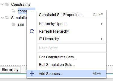
Step 9:
Go to “Add Sources” under the Flow Navigator -> PROJECT MANAGER window, select the “Add or create constraints” and click “Next”. Click on “Create file” and give a name for the XDC and select “File type” as “XDC”. Click “OK” and “Finish”.
Step 10:
Copy the following constraints to the newly created constraints file:
set_property -dict { PACKAGE_PIN K18   IOSTANDARD LVDS } [get_ports { clk_p }];
set_property -dict { PACKAGE_PIN J18   IOSTANDARD LVDS } [get_ports { clk_n }];
create_clock -add -name sys_clk_pin -period 10.00 [get_ports clk_p];

set_property -dict { PACKAGE_PIN L6   IOSTANDARD LVCMOS33   SLEW FAST} [get_ports { LED_out[7] }]; # Sch = 7SEG_7 (DP)
set_property -dict { PACKAGE_PIN L5   IOSTANDARD LVCMOS33   SLEW FAST} [get_ports { LED_out[6] }]; # Sch = 7SEG_6 (A)
set_property -dict { PACKAGE_PIN K5   IOSTANDARD LVCMOS33   SLEW FAST} [get_ports { LED_out[5] }]; # Sch = 7SEG_5 (B)
set_property -dict { PACKAGE_PIN K4   IOSTANDARD LVCMOS33   SLEW FAST} [get_ports { LED_out[4] }]; # Sch = 7SEG_4 (C)
set_property -dict { PACKAGE_PIN K6   IOSTANDARD LVCMOS33   SLEW FAST} [get_ports { LED_out[3] }]; # Sch = 7SEG_3 (D)
set_property -dict { PACKAGE_PIN J6   IOSTANDARD LVCMOS33   SLEW FAST} [get_ports { LED_out[2] }]; # Sch = 7SEG_2 (E)
set_property -dict { PACKAGE_PIN H6   IOSTANDARD LVCMOS33   SLEW FAST} [get_ports { LED_out[1] }]; # Sch = 7SEG_1 (F)
set_property -dict { PACKAGE_PIN G5   IOSTANDARD LVCMOS33   SLEW FAST} [get_ports { LED_out[0] }]; # Sch = 7SEG_0 (G)

set_property -dict { PACKAGE_PIN H5   IOSTANDARD LVCMOS33   SLEW FAST} [get_ports { DIG[0] }]; # Sch = 7_SEG1_EN (Thousands digit)
set_property -dict { PACKAGE_PIN H4   IOSTANDARD LVCMOS33   SLEW FAST} [get_ports { DIG[1] }]; # Sch = 7_SEG2_EN (Hundreds digit)
set_property -dict { PACKAGE_PIN J4   IOSTANDARD LVCMOS33   SLEW FAST} [get_ports { DIG[2] }]; # Sch = 7_SEG3_EN (Tens digit)
set_property -dict { PACKAGE_PIN J3   IOSTANDARD LVCMOS33   SLEW FAST} [get_ports { DIG[3] }]; # Sch = 7_SEG4_EN (Ones digit)
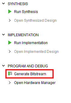
Step 11:
In Flow Navigator panel, click “Generate Bitstream” to synthesize, implement and to generate bitstream.
Step 12:
To program the Mimas AU-Plus with the generated bitstream, follow the steps mentioned below:
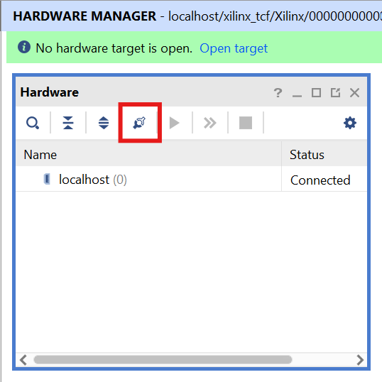
- Once the Bitstream is generated successfully, expand the “Open Hardware Manager” under “PROGRAM AND DEBUG” section of Flow Navigator panel.
- Then click “Open Target->Auto Connect”.
Then, Right Click on xcau7p_0(1) -> Program device.
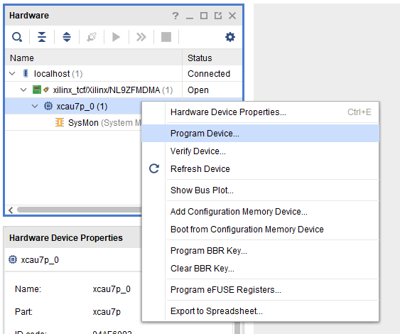
Dialog window for programming will open. Program the bit file by clicking ‘Program’.
Output :
You will notice the Seven Segment Display on the Mimas AU-Plus FPGA Development board will start counting from 0 to 1000.