Introduction
In this article, we’ll explore the process of creating an SD card test project using Vivado and Vitis Unified IDE for the Mimas AU-Plus FPGA Development Board. Our design will feature a MicroBlaze soft processor, which will be integrated with an SD card interface via the AXI bus and an SD card expansion module. This project will allow us to perform basic read and write operations on the SD card, helping to verify the functionality of the SD card interface on the Mimas AU-Plus. Although MicroBlaze designs can utilize either PLB or AXI bus systems, we’ll focus on the AXI bus for this tutorial. For detailed information on MicroBlaze and additional resources, including the datasheet, please visit AMD’s dedicated MicroBlaze page.
Prerequisites:
Hardware:
- Mimas AU-Plus Development board
- SD Card Expansion Module.
- SD card.
- USB Type C cable.
Software:
- Vivado Design Suite 2025.1
- Vitis Unified IDE 2025.1
Creating Microblaze based Hardware Platform for Mimas AU-Plus Development Board
The following steps will walk you through the process of creating a new project with Vivado and building a hardware platform with MicroBlaze soft processor using an IP integrator. Numato Lab’s Mimas AU-Plus FPGA Development Board is used in this example, but any compatible FPGA platform can be used with minor changes to the steps. Screenshots are added wherever possible to make the process easier for the reader.
Step 1:
Download and install Vivado Board Support Package files for Mimas AU-Plus from here.
Step 2:
Start Vivado Design Suite, and select “Create Project” from Quick Start section.
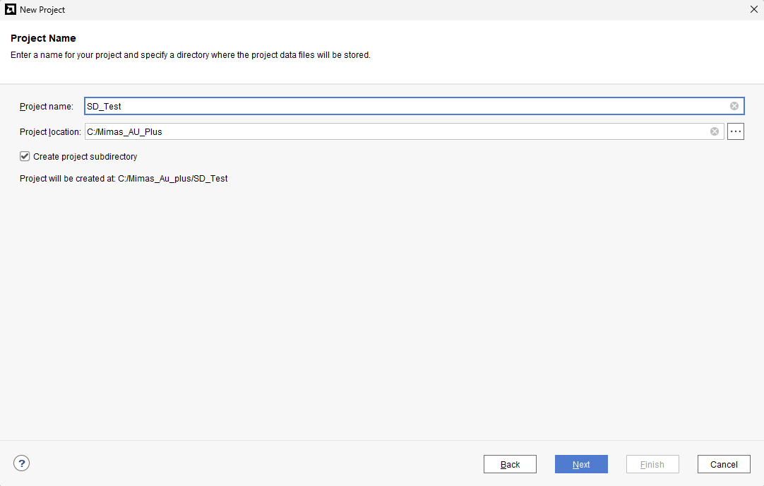
Step 3:
Enter a name for the project and save it at a suitable location. Check the option “Create project subdirectory”. Click Next to continue.
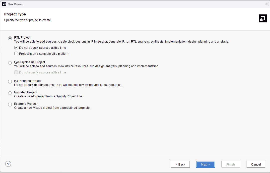
Step 4:
In the Project Type window, select RTL Project and check the option “Do not specify sources at this time”. Click Next.
Step 5:
In the Default Part window, select “Mimas_AU_Plus_dev_VA0.0” from the Boards option. If Mimas_AU_Plus_dev_VA0.0 is not listed, make sure board support files are installed correctly. Click Next to continue.
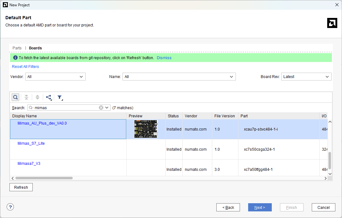
Click Finish to complete creating a new project. A new project will be created by Vivado with the selected settings.
Step 6:
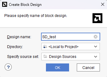
In the Flow Navigator panel, select Create Block Design under IP INTEGRATOR. Enter a name for the block design and click OK. An empty block design will be created.
Step 7:
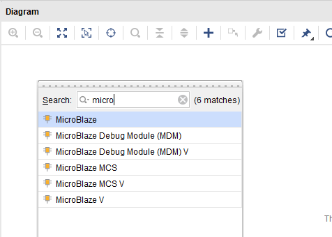
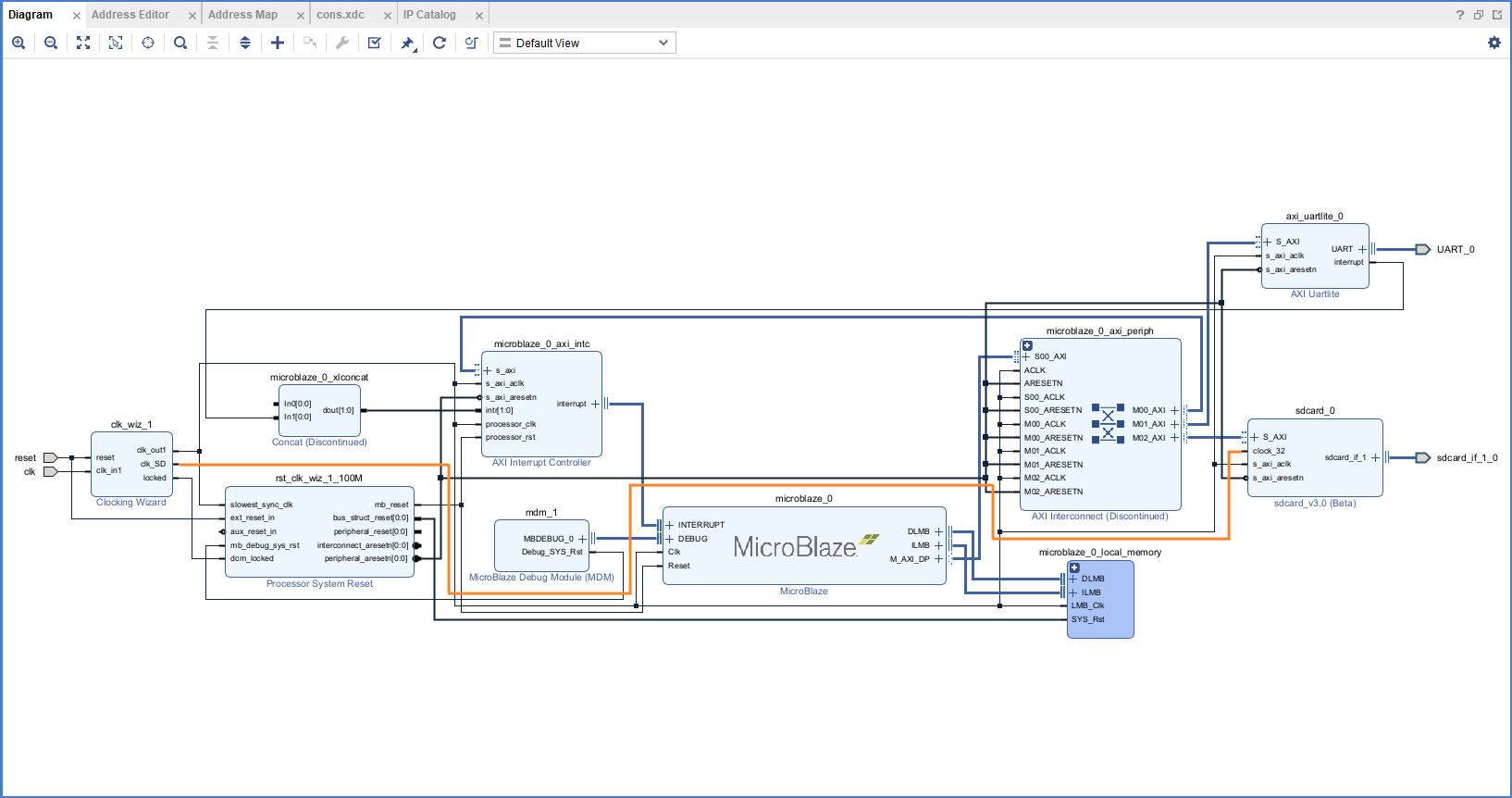
Go to Diagram window, right click and select “Add IP” from the popup menu. Search for “MicroBlaze” and add it to the design by double-clicking it.
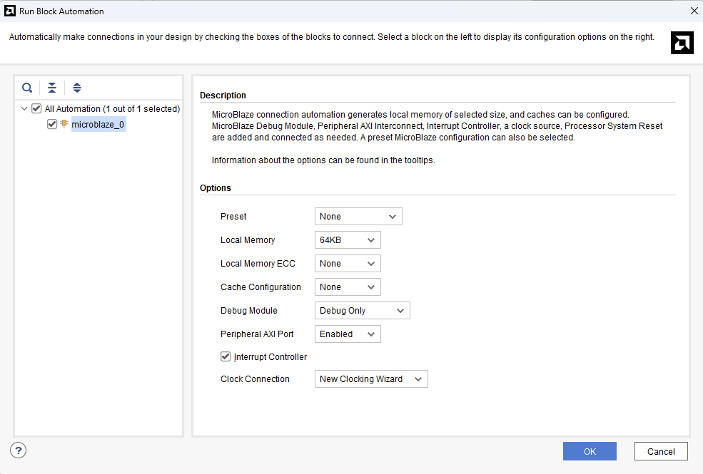
Click “Run Block Automation” present in the “Designer Assistance available” bar on the top left corner of the window to complete the design. Select the settings as shown in the following image. Click “OK” for Vivado to automatically configure the blocks for you.
Step 8:
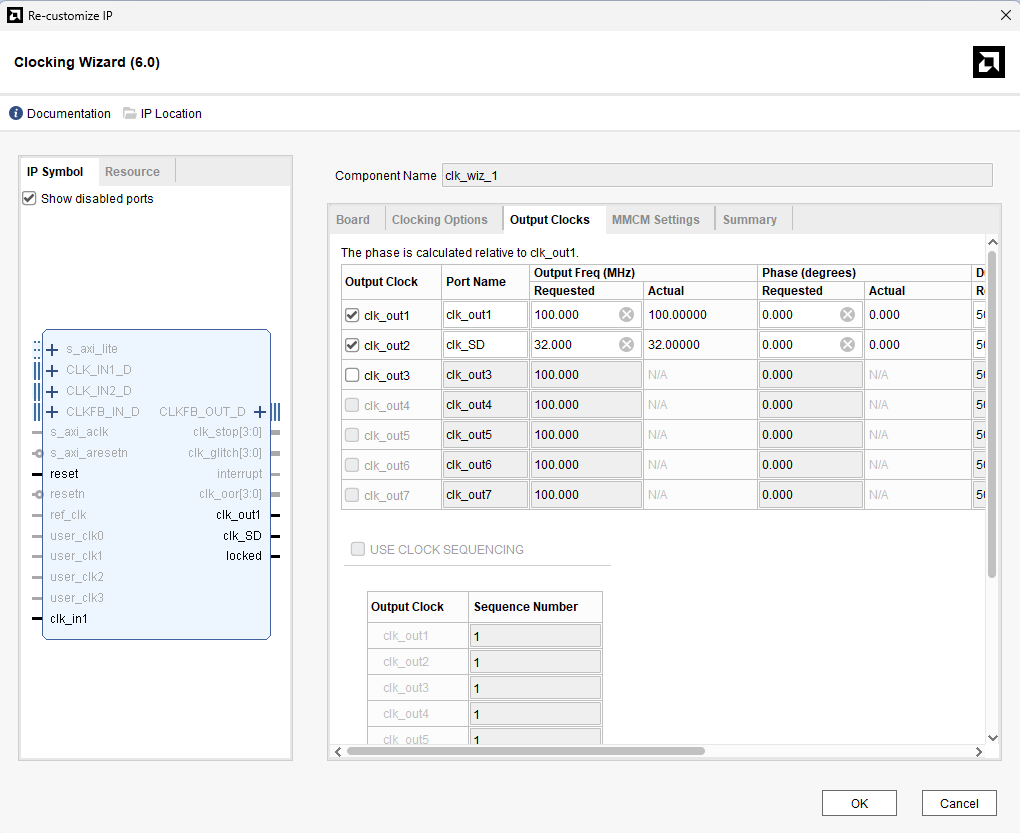
Double click “Clocking Wizard” IP and customize “Output Clocks” settings as shown in the following image.
Step 9:
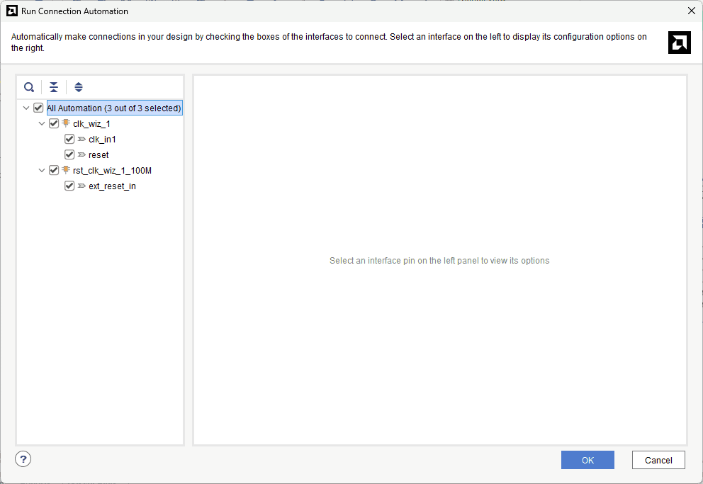
Run “Connection Automation” and select all the pins.
Step 10:
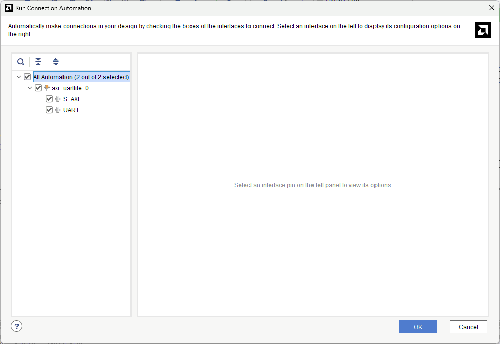
Select “Add IP” from the popup menu. Search for “AXI Uartlite” and add it to the design by double-clicking it. Click on “Run Connection Automation” select all the pins and Click ok.
Step 11:
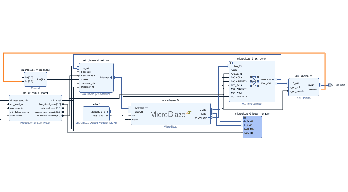
Connect interrupt output lines from “AXI Uartlite” to the “Concat” block as shown in the below figure.
 Step 12:
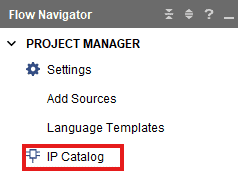
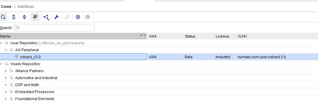
Add the SD card IP repository to Vivado IP catalog from here.
Open IP Catalog under PROJECT MANAGER, right click on Vivado Repository -> Add
Repository.
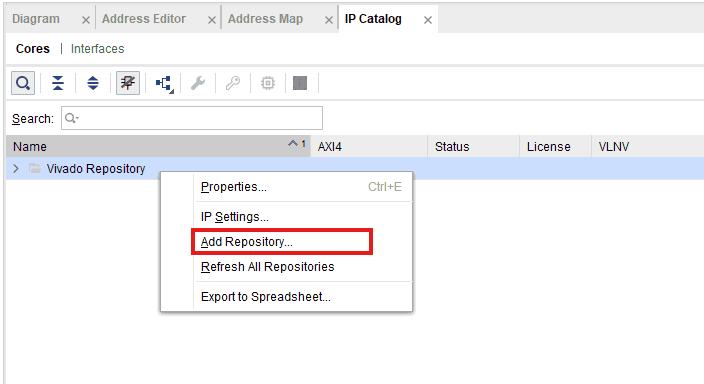
Provide the Directory path of the IP and click Select.
And Add the SDcard IP to the Block Design.
Step 13 :
After adding the SD card Ip to the Block design, click on Run Block Automation.
Now, connect the clock_32 pin of the SD card IP to the clk_SD pin of the Clocking wizard as shown in the below figure.
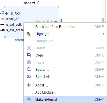
Step 14 :
Right click on Sdcard_if_1 and click on Make External.
Step 15 :
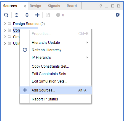
In Sources tab of Vivado, Right-Click on ‘Constraints’ and click ‘Add Sources’.
Step 16:
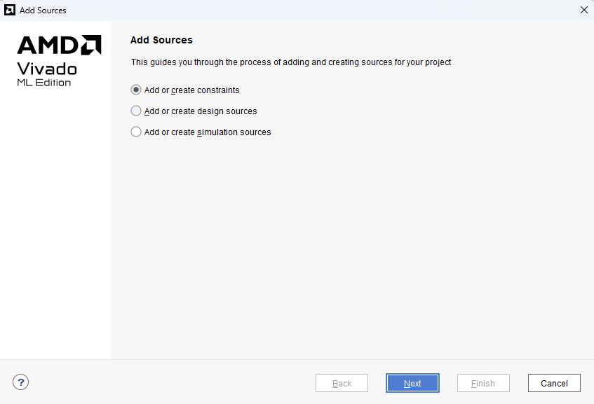
Once the “Add Sources” tab opens select “Add or create constraints” and click on “Next“.
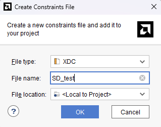
Click on ‘Create File’ and give ‘SD_test’ as File name. Click ‘OK’ and ‘Finish’.
Step 17:
Copy the following constraints in your constrains file and save it.
set_property -dict {PACKAGE_PIN P17 IOSTANDARD LVCMOS18} [get_ports sdcard_if_1_0_sd_clk]
set_property -dict {PACKAGE_PIN P16 IOSTANDARD LVCMOS18} [get_ports sdcard_if_1_0_sd_cs]
set_property -dict {PACKAGE_PIN R16 IOSTANDARD LVCMOS18} [get_ports sdcard_if_1_0_sd_miso]
set_property -dict {PACKAGE_PIN R17 IOSTANDARD LVCMOS18} [get_ports sdcard_if_1_0_sd_mosi]

set_property -dict {PACKAGE_PIN U14 IOSTANDARD LVCMOS33} [get_ports reset]
set_property -dict {PACKAGE_PIN K18 IOSTANDARD LVCMOS18} [get_ports clk]


set_property IOSTANDARD LVCMOS33 [get_ports UART_0_rxd]
set_property IOSTANDARD LVCMOS33 [get_ports UART_0_txd]
set_property PACKAGE_PIN Y6 [get_ports UART_0_rxd]
set_property PACKAGE_PIN AB7 [get_ports UART_0_txd]
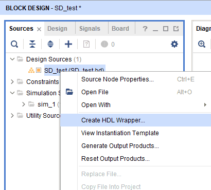
Step 18:
Right-click “SD_test” in the “Sources” window, and select “Create HDL Wrapper” from the popup menu. Click “OK” on the window that appears to finish generating a wrapper.
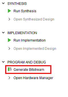
Step 19:
Click “Generate Bitstream” under the “Program And Debug” section to synthesize, implement and generate a bitstream.
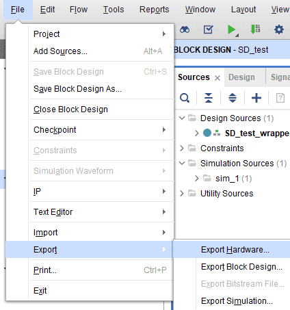
Step 20:
After generating the bitstream successfully, select Export -> Export Hardware from the File menu. Click Next.
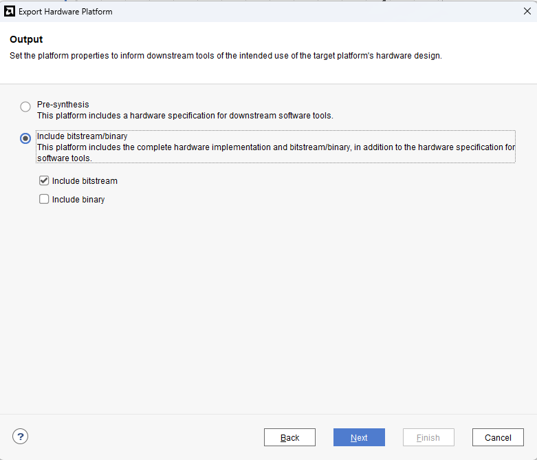
Select the “include bitstream” checkbox and click Next.
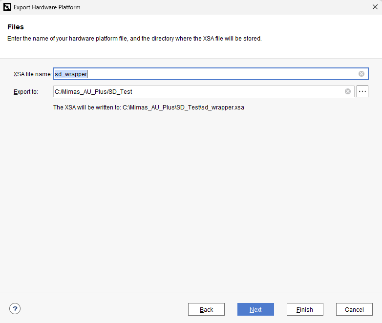
Provide the XSA file name and save it at a suitable location. Click Next and click Finish in the next dialog box.
Step 21:
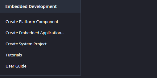
Launch Vitis IDE and create a new platform for the project, by selecting “Create Platform Component”, click “Next”, in the Flow tab select the XSA file saved using the step 15 and finally click “Next” and “Finish” respectively.
Step 22:
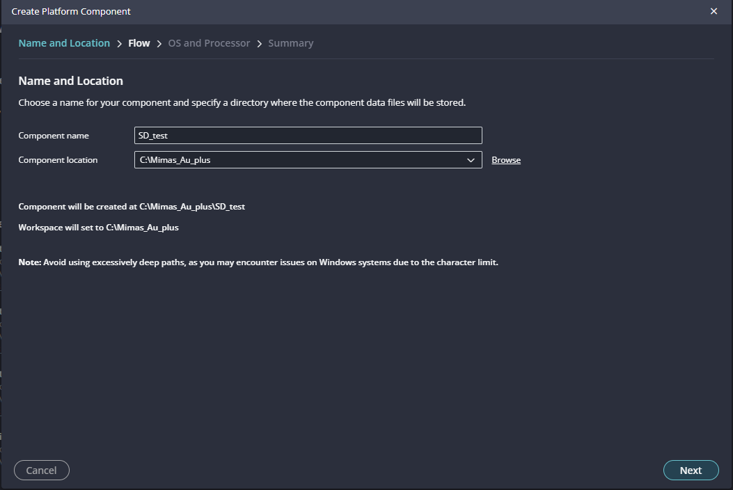
Give the component name and the platform location and click on “Next”.
Step 23:
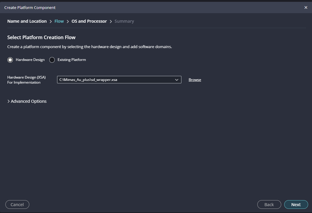
In the next tab browse the XSA file , select it , click on “Next”. In the next OS and Processor tab click “Next” and “Finish”.
After successful creation of the platform, build the platform.
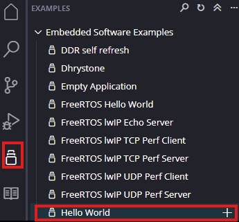
Step 24:
Next create an Application component by selecting the “Hello World” template from the “examples”.
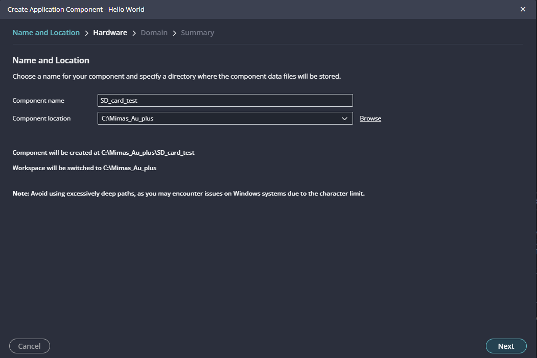
In “Create Application Component” tab specify project name and location, click “Next”.
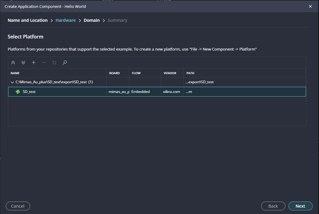
Select newly created Platform and click “Next”.
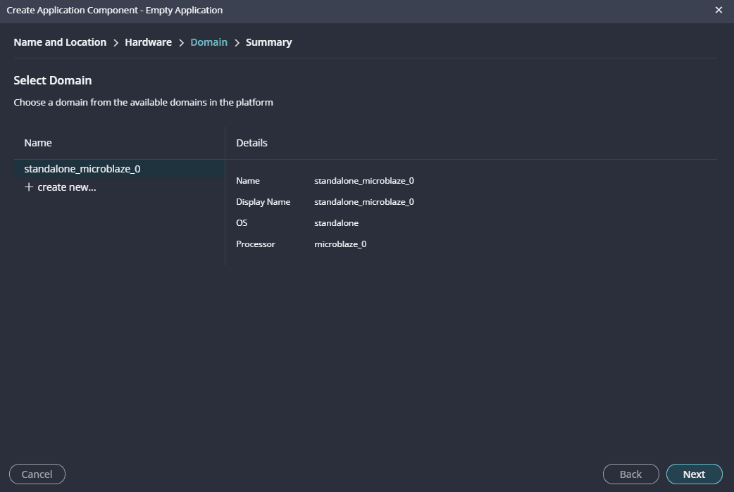
Select the domain as “Standalone_microblaze_0” and click “Next” and click on “Finish”
Step 25:
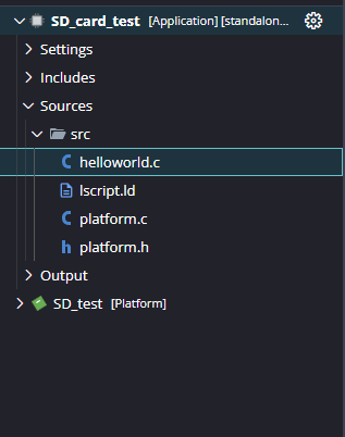
Go to the SD_card_test Applications ‘helloworld.c’ file under the ‘Sources’ tab and replace the code with the code given below to test SD card .
#include <stdio.h>
#include "xparameters.h"
#include "xil_types.h"
#include "xstatus.h"
#include "xil_testmem.h"


#include "xil_io.h"

#include "platform.h"
// #include "memory_config.h"
#include "xil_printf.h"

/* SD Card defines */
#define Card_Not_Found            0x04
#define Card_Version_x1           0x01
#define Card_Version_x2           0x02
/* SD Card */


void delay(uint32_t);
void putnum(unsigned int num);


int test_sdcard() {
    print("\r\n\r\n\e[1;33mMicroSD Card Test\e[0m\r\n");
    print("\e[1;33m*****************\e[0m\r\n\r\n");

    unsigned int i = 0xffffff;
    while (i--) {
    }

    u32 baseaddr;
    u32 DataRead;

    baseaddr = XPAR_SDCARD_0_BASEADDR;

    Xil_Out32((baseaddr) + (0x00) + (0x00), (u32)0x00);

    DataRead = 0;
    DataRead = Xil_In32((baseaddr) + (0x04) + (0x00));

    if (DataRead == Card_Not_Found) {
        print("\e[1;31mERROR:\e[0m Card Found! Error occurred \r\n\r\n");
        return -1;
    } else if (DataRead == Card_Version_x1) {
        print("\e[1;32mPASSED:\e[0m Card Found! Card inserted is of version \e[1;32mx1\e[0m\r\n");
    } else if (DataRead == Card_Version_x2) {
        print("\e[1;32mPASSED:\e[0m Card Found! Card inserted is of version \e[1;32mx2\e[0m\r\n");
    } else if (DataRead == 0x00) {
        print("\e[1;31mERROR:\e[0m SD Card not inserted!!\r\n");
        return -2;
    }

    print("SD Card Test Finished.\r\n");
    Xil_Out32((baseaddr) + (0x00000004) + (0x00), (u32)(0x01));

    print("\n\r");
    return 0;
}

int main() {
    init_platform();


    print("\r\n\r\n\e[1;36mMIMAS AU+ SD Card Test Suite\e[0m\r\n");
    print("\e[1;36m_____________________\e[0m\r\n\r\n");


    printf("Welcome to MIMAS AU+ SD Card Test Suite\r\n\n");

    // Run SD Card test
    test_sdcard();

    print("\r\n\r\nMIMAS AU+ SD Card Test Finished. Thank You.\r\n\n");
    cleanup_platform();
    return 0;
}
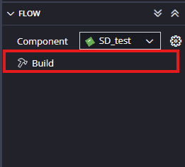
After adding the source file build the Project.
Step 26:
Once the Project is Built, Set up the hardware for testing the design. For this, Connect ‘Header P1 ’ of SD Card Module to ‘Header P7’ of Mimas AU Plus and insert the SD card in the SD card slot of the Expansion Module. Finally, connect USB type ‘C’ Cable for powering up Mimas AU Plus.
Step 27:
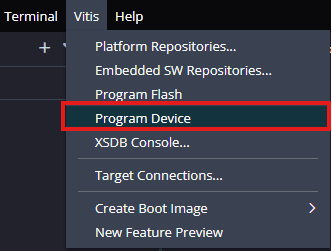
Program the FPGA on Mimas AU Plus with a simple boot loop program by selecting the Program Device option from the Vitis menu.
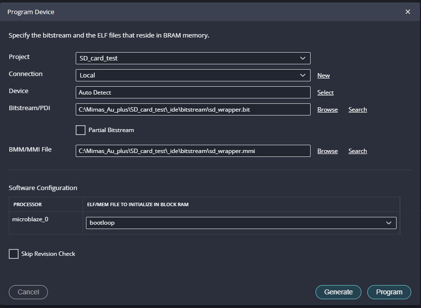
Once the “Program Device” window opens click on “Program“.
Step 28:
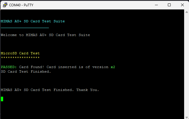
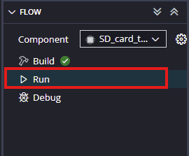
Meanwhile, open any serial terminal program (such as PuTTY, Teraterm etc) and open the port corresponding to Mimas AU Plus with a 9600 baud rate (the default baud rate given in UART IP). Program the board by selecting the “Run”.
Step 29:
If everything went well, Serial terminal would show the execution is Successful.