Introduction:
The FTDI FT2232H USB chip on-board Mimas AU-Plus provides users with a FIFO interface for data transfer between FPGA and host PC. The FT2232H chip features two channels or ports, which can be configured into various modes like UART, FIFO, JTAG etc. On Mimas AU-Plus, Channel A is used for FPGA configuration and flash programming, whereas channel B is for custom usage. This article demonstrates communication between host and the board using Asynchronous FIFO mode via boards’ respective channels of FT2232H. The Channel B of FT2232H in case of Mimas AU-Plus, when configured as FIFO, acts as a USB-FIFO bridge between host and FPGA.
Prerequisites
To follow this article, you would need the following:
- Hardware:
- Mimas AU-Plus FPGA Module
- AMD Platform Cable II JTAG debugger.
- Software:
- Vivado Design Suite 2025.1
- FT_Prog tool for configuring on-board FT2232H USB Serial converter (download and install from FTDI website)
- python 3.12
Let’s get started
The following steps will walk you through the process of creating a new project with Vivado . This article is written for Numato Lab’s Mimas AU-Plus Development Board. Screenshots are added wherever possible to make the process easier to the reader.
Step 1:
Download and install Vivado Board Support Package files for Mimas AU-Plus from here.
Step 2:
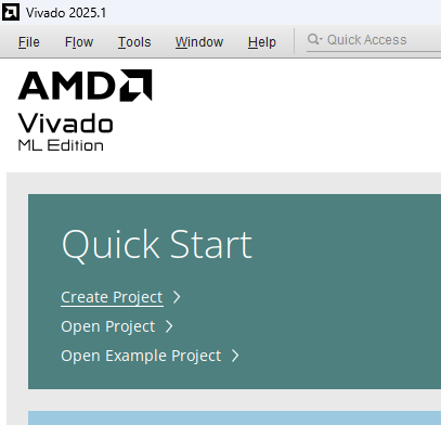
Start Vivado Design Suite, and select “Create Project” from Quick Start section. The project wizard will pop up. Press next to proceed with creating the project.
Step 3:
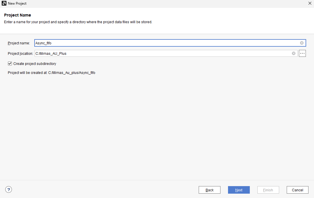
Type in a project name and save it at a convenient location. For this example “Async_fifo” is used as project name, but feel free to use any name. Select the check box below to keep all project files in a single folder. The image below shows the settings for the example project. Click “Next” to continue.
Step 4:
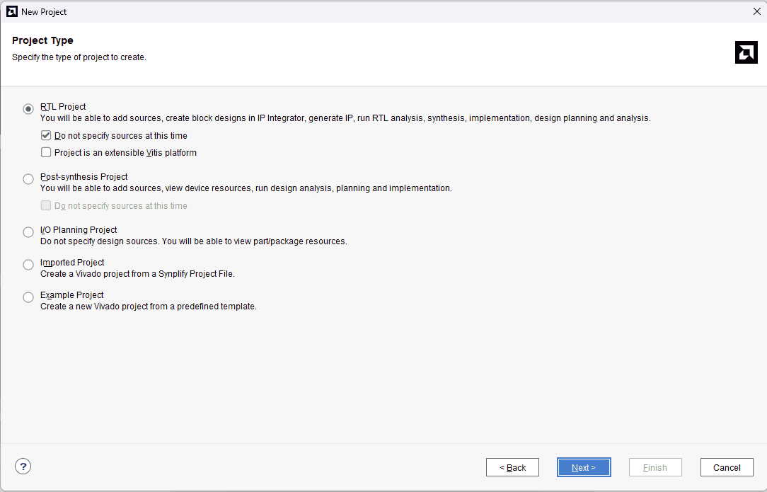
Choose “RTL Project” as project type and check the option “Do not specify sources at this time”.
Step 5:
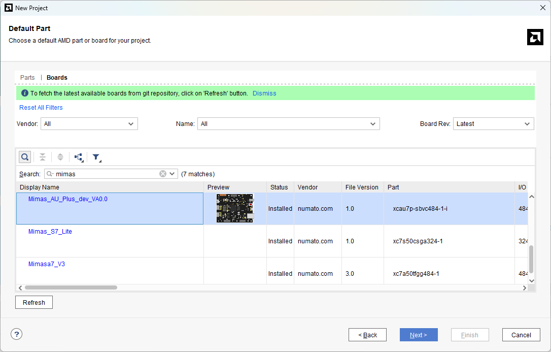
At the “Default Part” step, select “Boards” and choose Vendor as “numato.com”. Select “Mimas_AU_Plus_dev_VA0.0” and click “Next”. If Mimas_AU_Plus_dev_VA0.0 is not displayed in the boards list, you will need to install the board support files correctly.
Step 6:
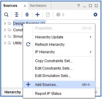
Right-Click on ‘Design Sources’ and select ‘Add Sources’. It will open a configuration window for adding Verilog files.
Step 7:
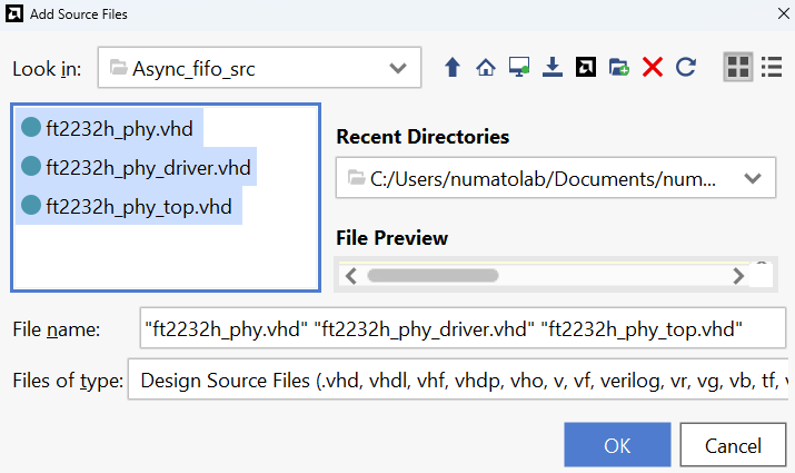
Download and extract the RTL source files from here. Click ‘Add Files’, select all files and add them to the project.
Here, FTDI’s Asynchronous FIFO interface is used to perform data transfer between FPGA and host PC. As the operation is asynchronous, the data transfers is not synchronous to any common clock between FPGA and FTDI. The design is simpler but has relatively lower speed than synchronous FIFO interface. To use the asynchronous FIFO transfer mode available on FT2232H, its hardware and driver must be configured as 245 FIFO and D2XX respectively. In this article, Channel B of FT2232H is configured as FIFO, which provides the following signals:
data: It is bi-directional bus carrying the 8-bit FIFO data.
rxf_n: It is an active low signal. When de-asserted, does not read data from FIFO. When it is enabled, it indicates that there is some data available in FIFO, the data is read after asserting rd_n.
txe_n: It is an active low signal. When de-asserted, does not write data to FIFO. When it is asserted, data can be written to FIFO if wr_n is asserted.
rd_n: It is an active low signal. When asserted, data is driven onto ‘data’ bus from FIFO.
wr_n: It is an active low signal. When asserted, data from ‘data’ bus is driven into FIFO.
In the RTL code, FSM is implemented which checks if there is some data available for reading (indicated by pending_read), then the data is read by enabling rd_n signal. When there is some data to be written (indicated by pending_write), wr_n signal is asserted and incoming data is driven into FIFO.
Step 8:
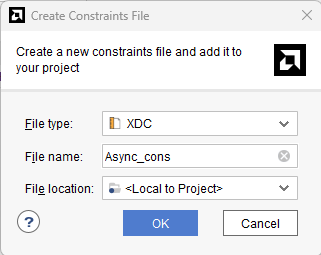
Right-Click on Constraints and select ‘Add sources’.
Step 9:
Click Next and then ‘Create File’. Enter a name for the constraints file and Click Finish.
Step 10:
Copy the following constraints to the newly created .xdc file.
set_property -dict { PACKAGE_PIN "Y6"     IOSTANDARD LVCMOS33    SLEW FAST } [get_ports {data[0]}];
set_property -dict { PACKAGE_PIN "AB7"    IOSTANDARD LVCMOS33    SLEW FAST } [get_ports {data[1]}];
set_property -dict { PACKAGE_PIN "AA7"    IOSTANDARD LVCMOS33    SLEW FAST } [get_ports {data[2]}];
set_property -dict { PACKAGE_PIN "AB8"    IOSTANDARD LVCMOS33    SLEW FAST } [get_ports {data[3]}];
set_property -dict { PACKAGE_PIN "AA8"    IOSTANDARD LVCMOS33    SLEW FAST } [get_ports {data[4]}];
set_property -dict { PACKAGE_PIN "AB9"    IOSTANDARD LVCMOS33    SLEW FAST } [get_ports {data[5]}];
set_property -dict { PACKAGE_PIN "Y10"    IOSTANDARD LVCMOS33    SLEW FAST } [get_ports {data[6]}];
set_property -dict { PACKAGE_PIN "AB10"   IOSTANDARD LVCMOS33    SLEW FAST } [get_ports {data[7]}];
set_property -dict { PACKAGE_PIN "V9"     IOSTANDARD LVCMOS33    SLEW FAST } [get_ports {rxf_n}] ;
set_property -dict { PACKAGE_PIN "Y8"     IOSTANDARD LVCMOS33    SLEW FAST } [get_ports {txe_n}] ;
set_property -dict { PACKAGE_PIN "Y9"     IOSTANDARD LVCMOS33    SLEW FAST } [get_ports {rd_n}] ;
set_property -dict { PACKAGE_PIN "AA11"   IOSTANDARD LVCMOS33    SLEW FAST } [get_ports {wr_n}] ;
set_property -dict { PACKAGE_PIN "V6"     IOSTANDARD LVCMOS33    SLEW FAST } [get_ports {rst}] ;
set_property -dict { PACKAGE_PIN "K18"    IOSTANDARD LVCMOS18} [get_ports {clk}];
Step 11:
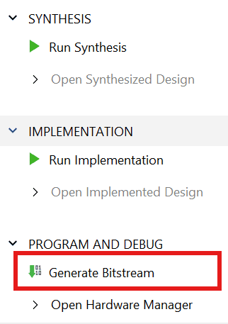
Click “Generate Bitstream” under PROGRAM AND DEBUG section and click “Yes” in any subsequent dialog window which comes up.
Step 12:
Once the bitstream is successfully generated, close any “Bitstream Generation Completed” dialog which comes up asking for what to do next.
Step 13:
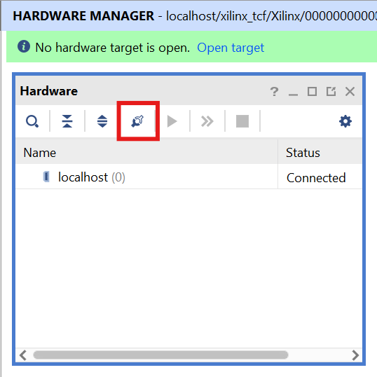
Click on “Open Hardware Manager” and then select “auto connect”.
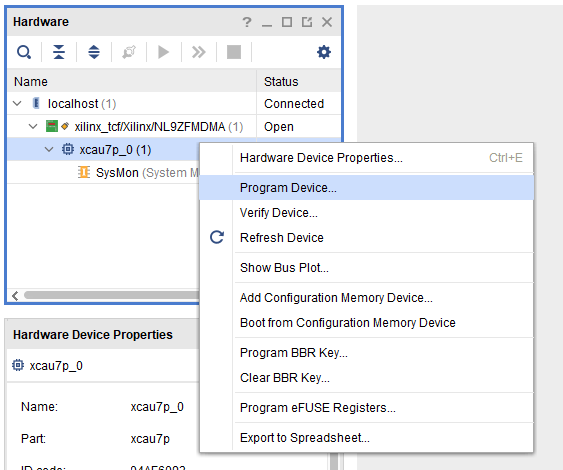
Then, Right Click on xcau7p_0(1) -> Program device.
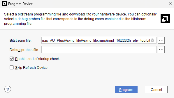
Dialog window for programming will open. Program the bit file by clicking ‘Program’.
Step 14:
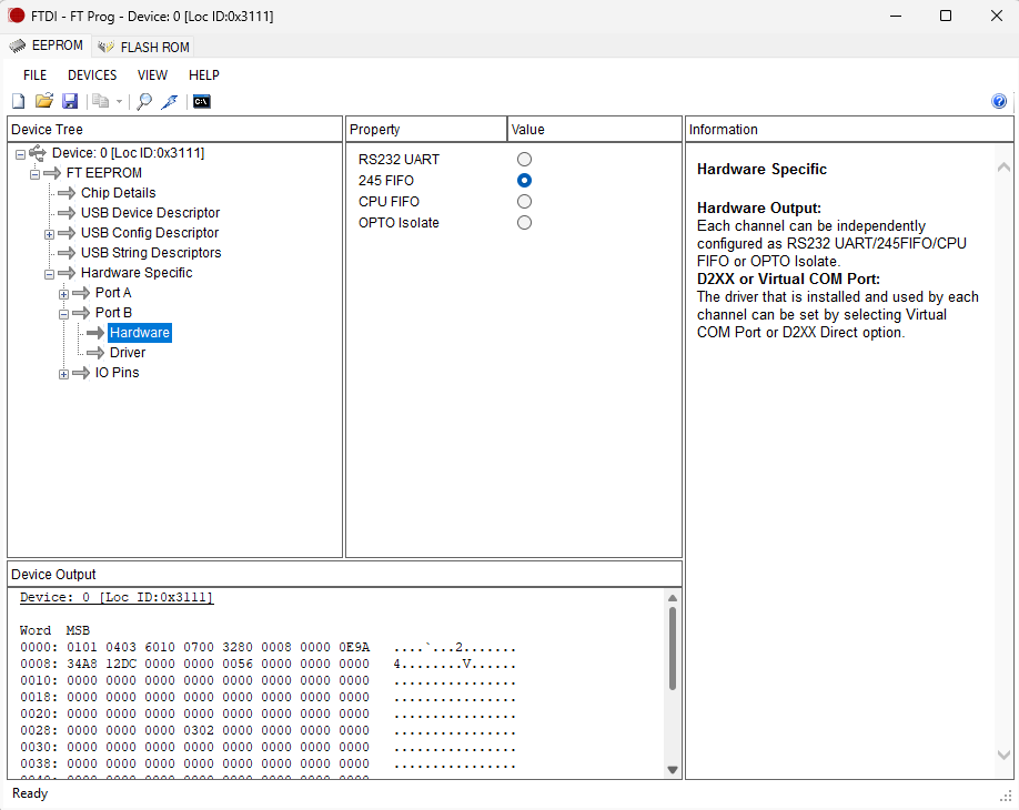
Once the device is programmed, program proper FTDI Settings for FIFO to work.
Change FT Prog settings as follows: Go to Device:0 -> Hardware Specific -> Port B -> Hardware and select 245 FIFO.
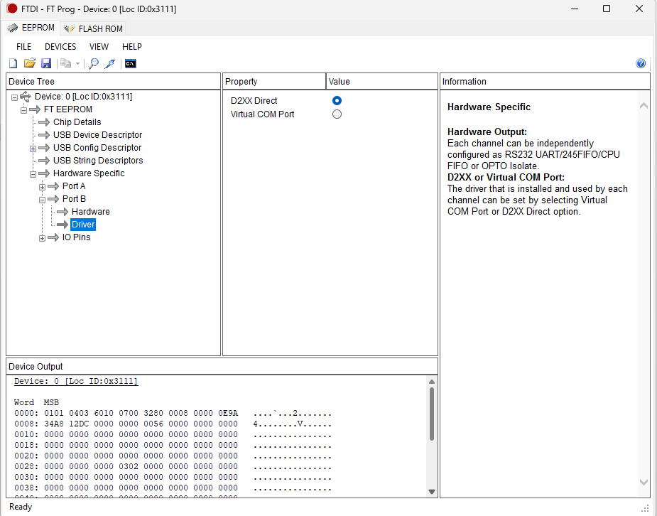
Now go to Hardware Specific -> Port B -> Driver and select D2XX Direct.
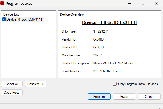
Then click on program device.
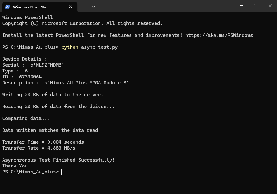
Step 15:
To check if Asynchronous FIFO is working as expected, write some data through FIFO, read it back and compare it. If the data written matches the data that is read then it means that the design is working fine.
To check this, copy the following python code in text editor and save it as ‘async_test.py’.
from __future__ import print_function

import time
import random

import ftd2xx


# Change device name in the next line according to your board

dev = ftd2xx.openEx(b'Mimas AU Plus FPGA Module B', 2)
dev.setTimeouts(5000, 5000)
dev.purge(ftd2xx.defines.PURGE_TX|ftd2xx.defines.PURGE_RX)
print("\nDevice Details :")
print("Serial : " , dev.getDeviceInfo()['serial'])
print("Type : " , dev.getDeviceInfo()['type'])
print("ID : " , dev.getDeviceInfo()['id'])
print("Description : " , dev.getDeviceInfo()['description'])

BLOCK_LEN = 2048 * 10

tx_data = bytes(bytearray([ random.randrange(0, 256) for i in range(BLOCK_LEN) ]))
print("\nWriting %d KB of data to the deivce..." % (BLOCK_LEN / 1024))
ts = time.time()
written = dev.write(tx_data)

rx_data = dev.read(BLOCK_LEN)
te = time.time()
print("\nReading %d KB of data from the deivce..." % (BLOCK_LEN / 1024))
p = te - ts

print("\nComparing data...\n")
if (tx_data == rx_data):
 print("Data written matches the data read\n")
else:
 print("Data verification failed\n")

dev.close()
print("Transfer Time = %.3f seconds" % p)
speed = (BLOCK_LEN / 1024./1024 / p)
print("Transfer Rate = %.3f MB/s" % speed)

print("\nAsynchronous Test Finished Successfully!\nThank You!!")
Step 16:
Open command prompt. Change to the directory of the file async_test.py and enter the following command:
python async_test.py