So far we learned a few things about Verilog and how to create a module in Verilog and run a simulation. While simulation can tell us a lot of things about the correctness of our module, there is nothing like putting it on a piece of hardware and seeing it working. In this part of the tutorial, we will walk you through the steps for synthesizing the module and implementing it on Elbert S7 hardware.
The test bench code is used only for simulation. To synthesize our module, we have to remove the test bench code. For those who don’t know, HDL Synthesis is the step where the HDL ( Verilog/VHDL or any other HDL for that matter) is interpreted and an equivalent hardware topology is generated. This hardware topology will be very specific to the target FPGA selected. Synthesis is a very complex process and we don’t need to know the internals to get our simple module up and running.
We will use the Elbert S7 to implement our module. Elbert S7 board has a AMD Spartan 7 FPGA, Four PMOD Header, and a few other peripherals on board. The exact FPGA part number used on this board is XC7S50-1CSGA324C. We will use two Switches and one LED to implement our logic.
Let’s come back to our module and think about how we can implement the same on the hardware. The module in question is an NAND gate. As we know, the output of an NAND gate is low only when both the inputs are high and the output is high if any of the inputs are low. We can have many possible hardware configurations to test this module. The easiest would be with a switch and an LED. See the proposed hardware configuration in the picture below.
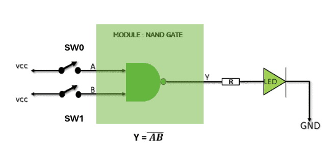
In the above diagram, two switches are connected as inputs. The output is connected to an LED. Let’s take a moment to understand how this circuit is going to behave. When the switch is in an open position, there will be a no voltage i.e., a logic 0 at the input of the NAND gate, and when the switch is closed position there will be Positive voltage at the input of the switch. In active High circuits like the one in Elbert S7, the switch is active when the input is high. When both the switches (Input A & B) are pressed at the same time the output (Y) will be low. If only one of the switches is pressed or if no switches are pressed then the output will be high.
Now we know the basic hardware requirements. We need the following in our prospective hardware.
- An input-capable IO with a switch attached.
- An output-capable IO with an LED attached.
We can now take a look at the Elbert S7 schematics and learn a little bit more about where the switches and LEDs are connected. We will use switches SW0 and SW1 and LED “LED0” for our purpose. Looking through the schematics reveals that switches SW0 and SW1 are connected to IO C4 and B4. LED0 is connected to V14 of the FPGA respectively.
We now have a Verilog module that we want to implement and we have selected a hardware platform and decided what IOs to use for implementation. Let us revisit our module.
module nand_gate (
input a,    // First input
input b,    // Second input
output reg y // Output defined as 'reg' for behavioral modeling
);

// Behavioral description using always block
always @(*) begin
if (a & b)
    y = 0;  // NAND logic: If both inputs are 1, output is 0
else
    y = 1;  // Otherwise, output is 1
end
endmodule
Our module has three ports. Port A and B are the input and Port Y, which is the output. An attentive reader would be asking now, how are we going to attach Port A and Port B to C4 and B4 of the hardware and Port Y to V14 of the hardware? We will do this by defining user constraints. User constraints tell the router and the placement logic (which is a part of the HDL synthesizer) on which physical pins of the module signals are to be connected. We make a list of constraints place it in a file and include that file in the project. This file is called a User Constraints File. For Xilinx Vivado tools, it is a text file with a .xdc extension.
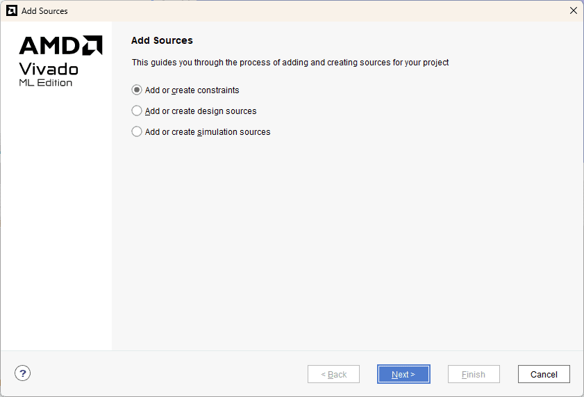
To create the constraints file, follow the steps below:
Step 1 :
Go to “Add Sources” under the Flow Navigator –> PROJECT MANAGER window, select the “Add or create constraints” and click “Next”.
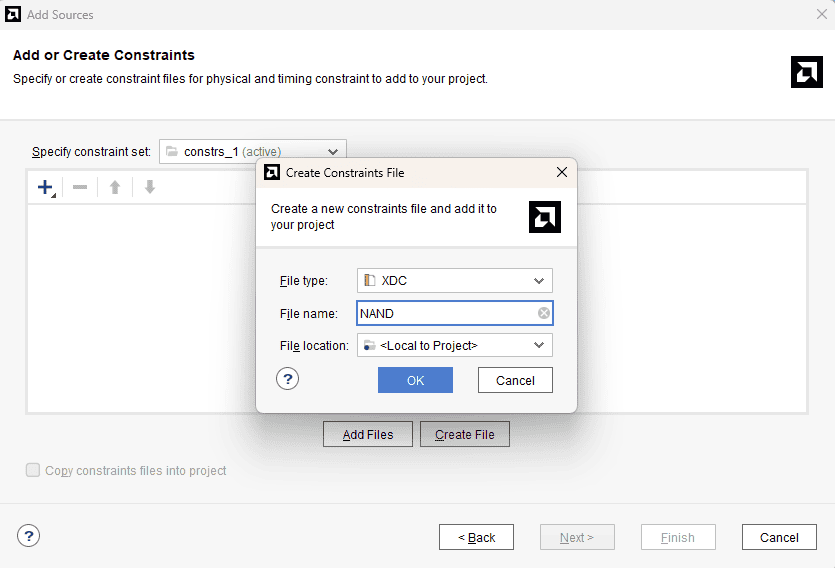
Step 2 :
Click on “Create file” and give a name for the XDC and select “File type” as “XDC”. Click “OK” and then “Finish”.
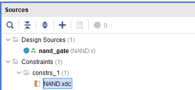
Step 3 :
The XDC file is now created and is available in the Sources –> Constraints. Double-click on it to open.
Now the constraints file for the project is created. The constraints used in our project are provided below. Copy and paste these constraints in the constraints file.
set_property -dict { PACKAGE_PIN "C4" IOSTANDARD LVCMOS33 SLEW FAST} [get_ports { a }];
set_property -dict { PACKAGE_PIN "B4" IOSTANDARD LVCMOS33 SLEW FAST} [get_ports { b }];
set_property -dict { PACKAGE_PIN "V14" IOSTANDARD LVCMOS33 SLEW FAST} [get_ports { y }];
Now we have pretty much everything we need to synthesize the design and test it.
Step 4 :
Right-click on “Generate Bitstream” in the Flow Navigator panel.
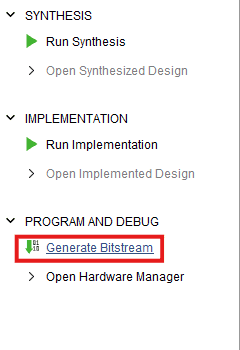
The bitstream generation process may take a while.
Step 5 :
Once the bitstream generation is completed, if everything goes well and there are no errors, the following window will be displayed.
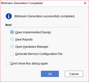
If there are any errors or warnings, you can check them in the “messages” window.
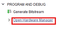
Step 6 :
To program the Elbert S7 with the generated bitstream, follow the steps mentioned below:
- Once the Bitstream is generated successfully, expand the “Open Hardware Manager” under “PROGRAM AND DEBUG” section of Flow Navigator panel.
- Then click “Open Target->Auto Connect”.
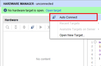
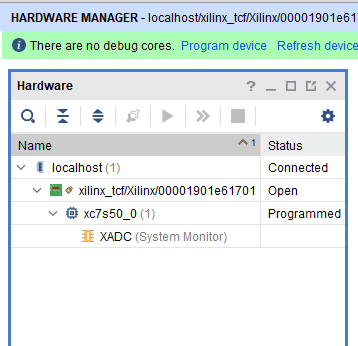
You can now see that the board is detected.
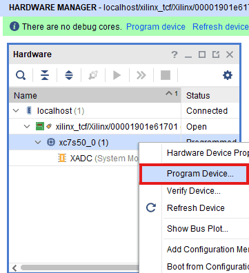
Now, right click on the device “xc7s50_0(1)”and click “Program Device”.
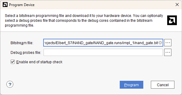
Select the NAND_gate out bitstream and click “Program”.
Once Programming is complete, Turn ON the switch SW0 and SW1 at the same time to see LED0 will go low.