Introduction
Testing DDR4 memory for Mimas AU-Plus FPGA Development board involves using specialized tools to ensure the memory functions correctly within the FPGA environment. In Vitis, a software development platform by AMD, a memory test template can be utilized to perform these tests. This template helps in validating the performance and reliability of DDR4 memory by running predefined test patterns and checking for errors. The Purpose of this article is to help readers to understand how to test DDR4 memory available on Mimas AU Plus FPGA Module using Memory tests template.
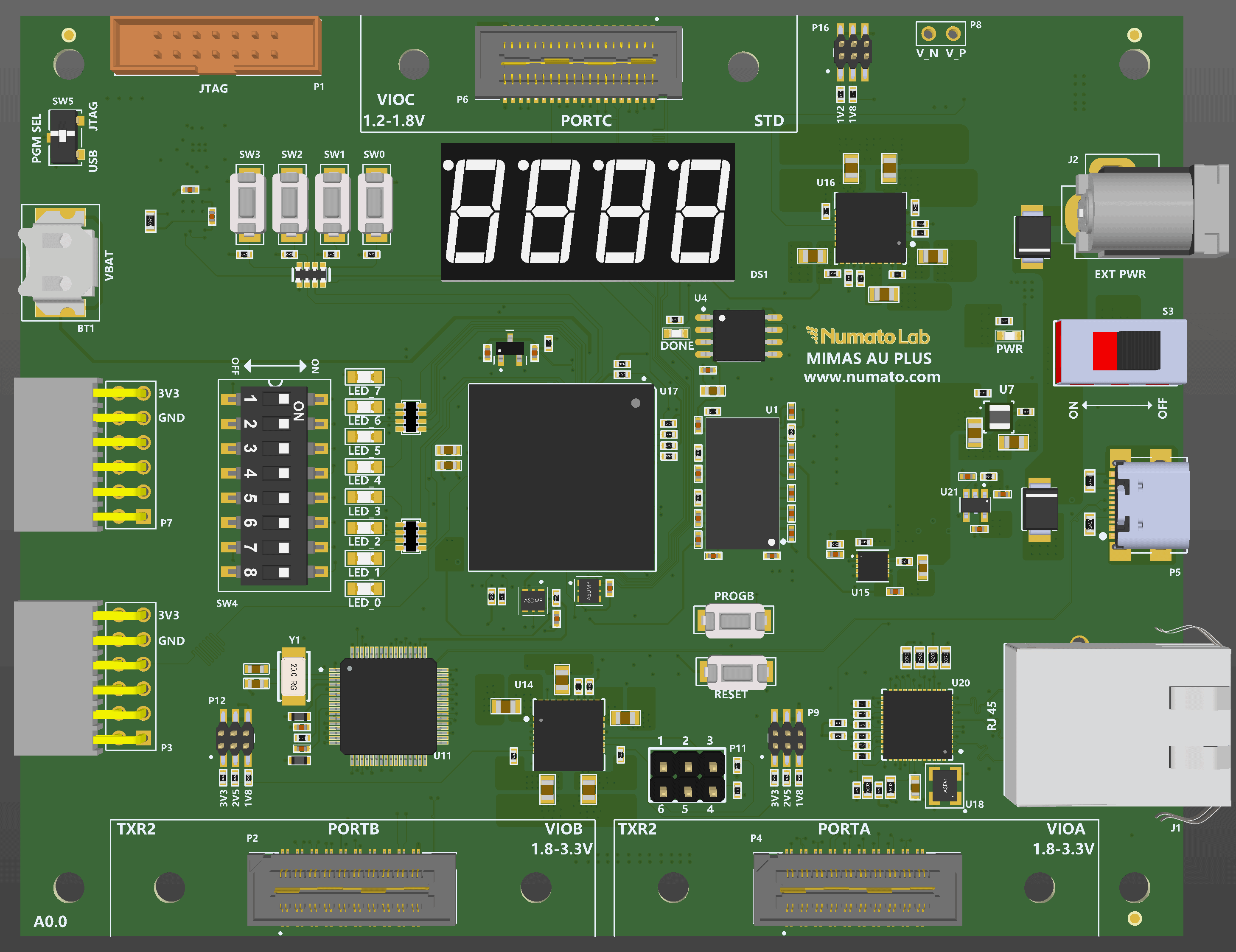
Mimas AU Plus FPGA Development Board
Mimas AU-Plus Development Module is an easy to use FPGA Development Module featuring Artix Ultrascale+ FPGA (XCAU7P-1SBVC484 package). The FT2232H brings versatile USB-to-serial connectivity, while DDR4 support enhances data processing efficiency. The inclusion of Gigabit Ethernet facilitates seamless networking, opening doors to IoT and cloud computing applications. Storage is swift and reliable with QSPI flash, while the M.2 M key interface embraces cutting-edge storage solutions and supports high-speed communication. The addition of PMOD connectors enhances flexibility, allowing easy interfacing with sensors and peripherals for customized projects.
In essence, the Mimas AU-Plus FPGA Development Module is a compact, feature-rich solution for FPGA development, empowering both seasoned developers and enthusiasts to explore limitless possibilities in embedded systems and digital design.
Prerequisites:
Hardware:
- Mimas AU Plus FPGA Development Board.
- AMD Platform Cable USB II JTAG debugger.
- USB Type C cable.
Software:
- Vivado Design Suite 2025.1
- Vitis Unified IDE 2025.1
Creating Microblaze based Hardware Platform for Mimas AU-Plus Development board
The following steps will walk you through the process of creating a new project with Vivado and building a hardware platform with MicroBlaze soft processor using an IP integrator. Numato Lab’s Mimas AU Plus FPGA Development Board is used in this example, but any compatible FPGA platform can be used with minor changes to the steps. Screenshots are added wherever possible to make the process easier for the reader.
Step 1:
Download and install Vivado Board Support Package files for Mimas AU Plus from here.
Step 2:
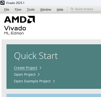
Start Vivado Design Suite, and select “Create Project” from Quick Start section. The project wizard will pop up. Press next to proceed with creating the project.
Step 3:
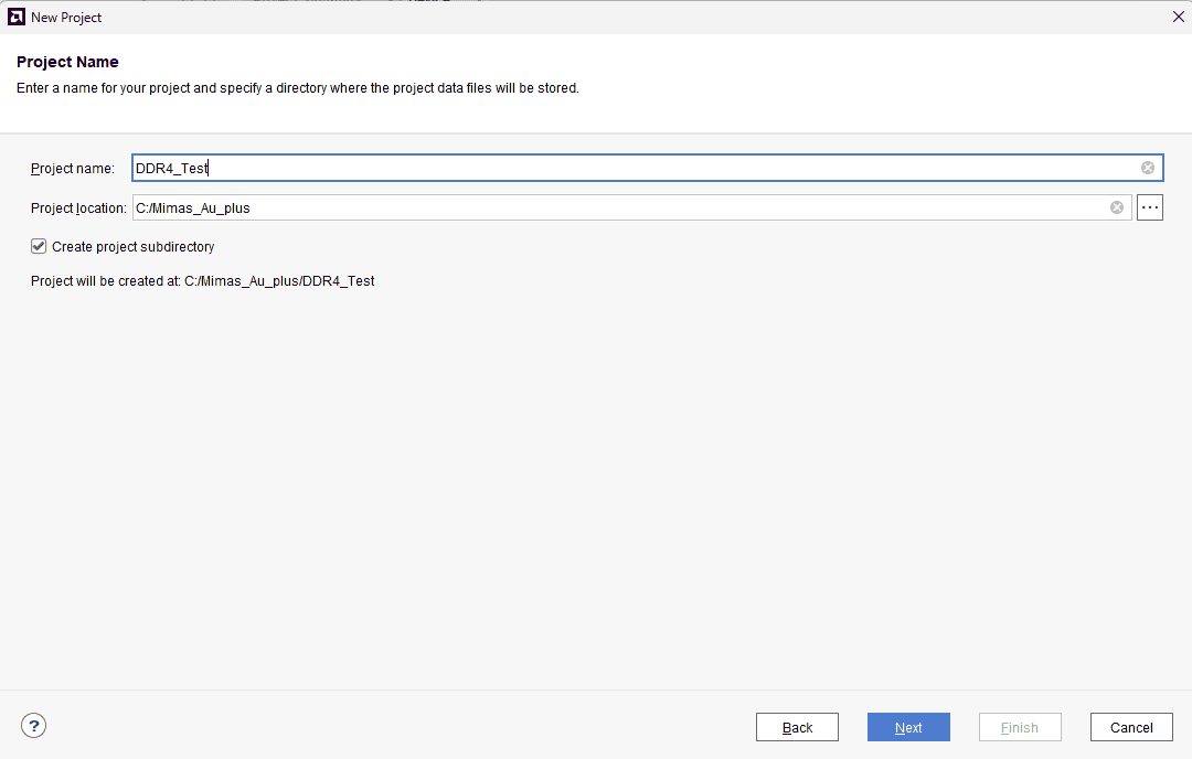
Enter a name for the project and save it at a suitable location. Check the option “Create project subdirectory”. Click Next to continue.
Step 4:
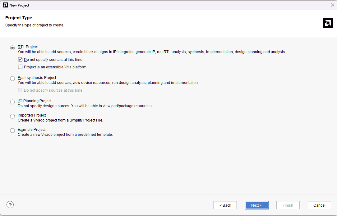
In the Project Type window, select RTL Project and check the option “Do not specify sources at this time”. Click Next.
Step 5:
In the Default Part window, select “Mimas_AU_Plus” from the Boards option. If not listed, make sure board support files are installed correctly. Click Next to continue.
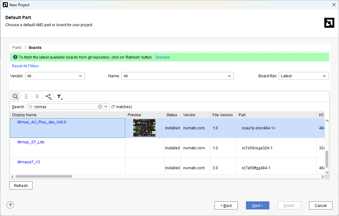
Click Finish to complete creating a new project. A new project will be created by Vivado with the selected settings.
Step 6:
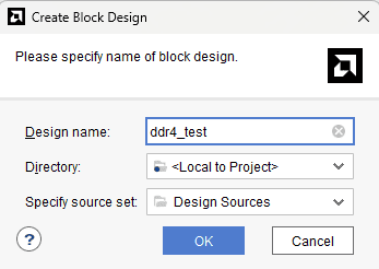
In the Flow Navigator panel, select Create Block Design under IP INTEGRATOR. Enter a name for the block design and click OK. An empty block design will be created.
Step 7:
Click the Board tab. The default peripherals available for the Mimas AU Plus board will be displayed.
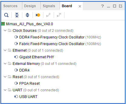
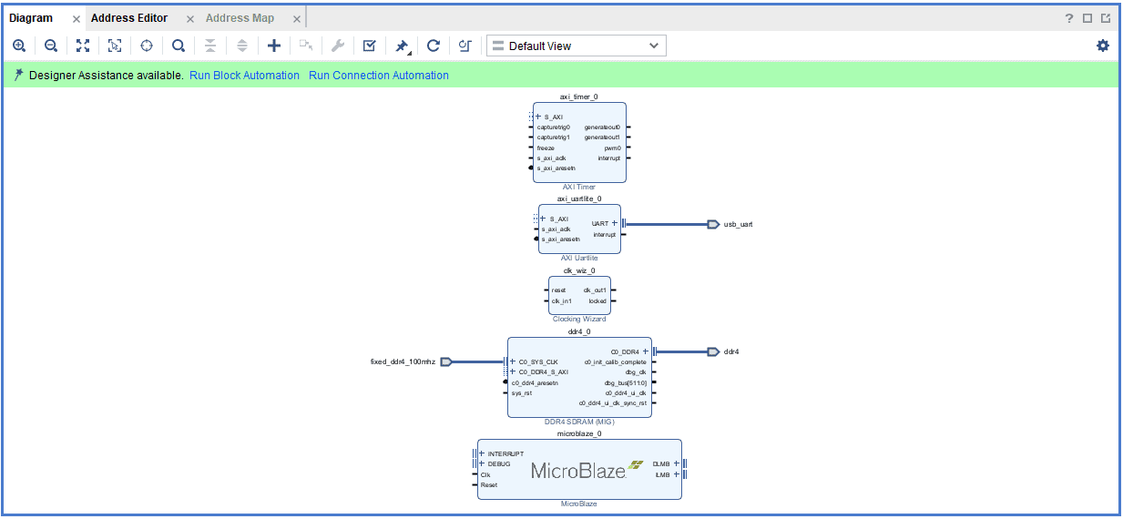
Step 8:
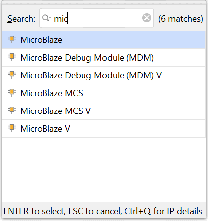
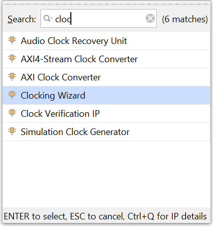
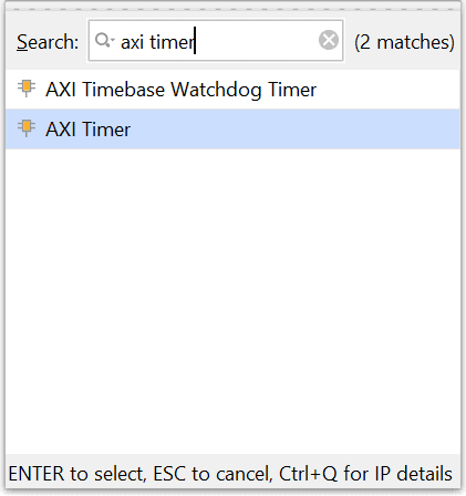
Add DDR4 and USB UART to the design by double-clicking the corresponding peripherals. In the Diagram window, right-click and select “Add IP” from the popup menu. Search for “MicroBlaze” ,”clocking wizard” & “AXI Timer” and add them to the design by double-clicking them.
Step 9:
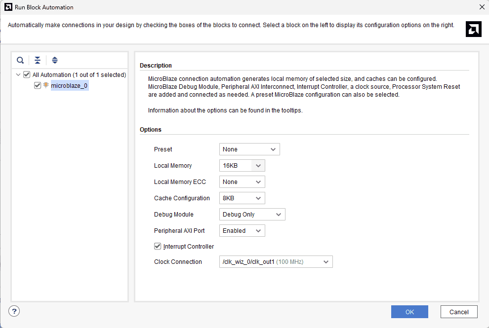
Click “Run Block Automation” present in the “Designer Assistance available” bar on the top left corner of the window to complete the design. Select the settings as shown in the following image. Click “OK” for Vivado to automatically configure the blocks for you. Once Block Automation is complete, run “Connection Automation” so Vivado can connect the blocks to make a complete system.
Enable the “Interrupt controller” in the Run Block Automation Window as below
Step 10:
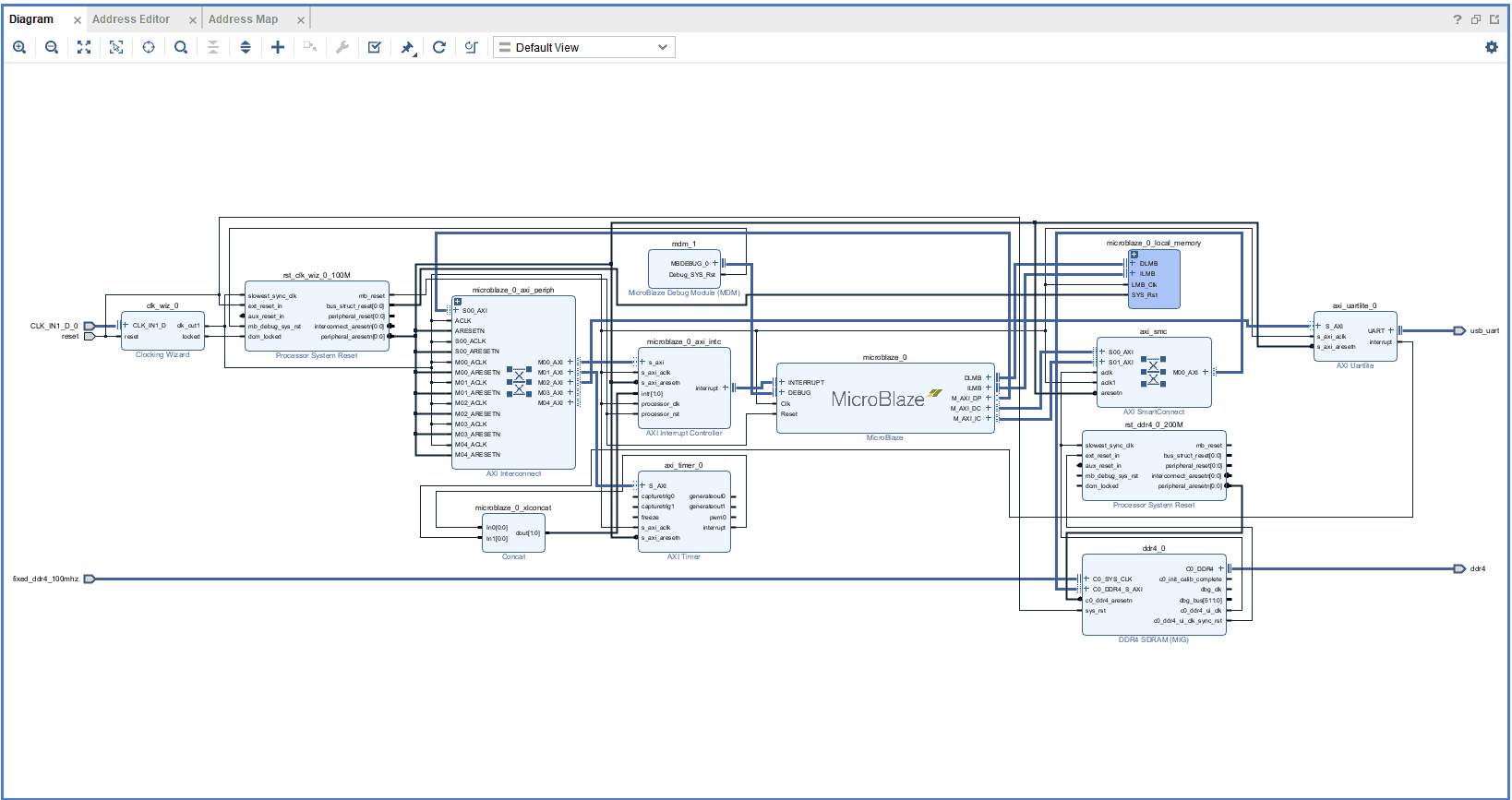
Connect interrupt output lines from “AXI Timer” and “UARTLite” to the “Concat” block as shown below figure. Select the “Validate Design” option from the Tools menu to make sure that connections are correct.
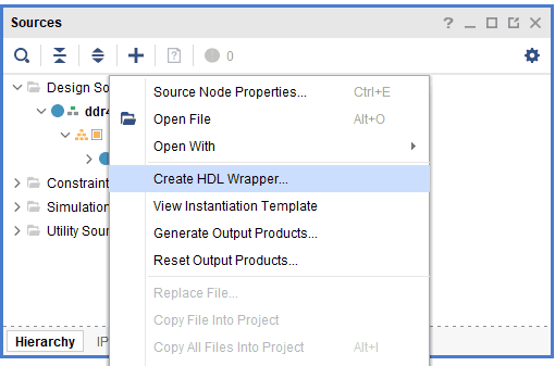
Step 11:
Right-click “ddr4_test” in the “Sources” window, and select “Create HDL Wrapper” from the popup menu. Click “OK” on the window that appears to finish generating a wrapper.
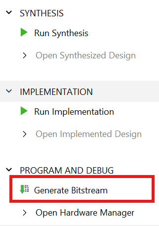
Step 12:
Click “Generate Bitstream” under the “Program And Debug” section to synthesize, implement and generate a bitstream.
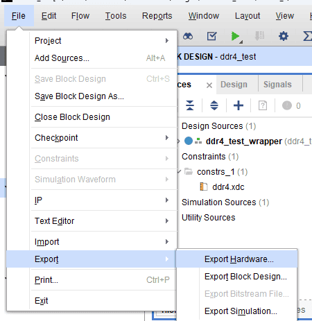
Step 13:
After generating the bitstream successfully, select Export -> Export Hardware from the File menu. Click Next.
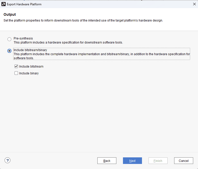
Select the “include bitstream” checkbox and click Next.
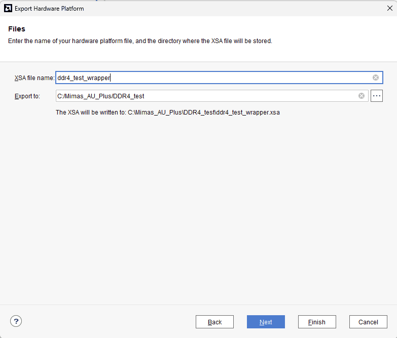
Provide the XSA file name and save it at a suitable location. Click Next and click Finish in the next dialog box.
Step 14:
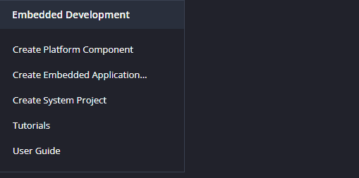
Launch Vitis IDE and create a new platform for the project, by selecting “Create Platform Component”, click “Next”, in the Flow tab select the XSA file saved using the step 15 and finally click “Next” and “Finish” respectively.
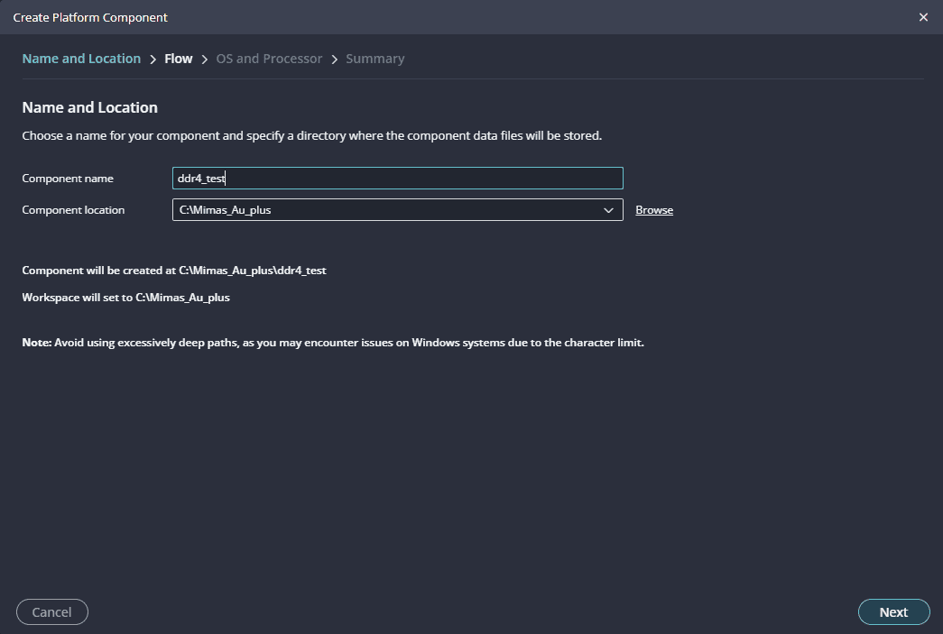
Step 15:
Give the component name and the platform location and click on “Next”.
Step 16:
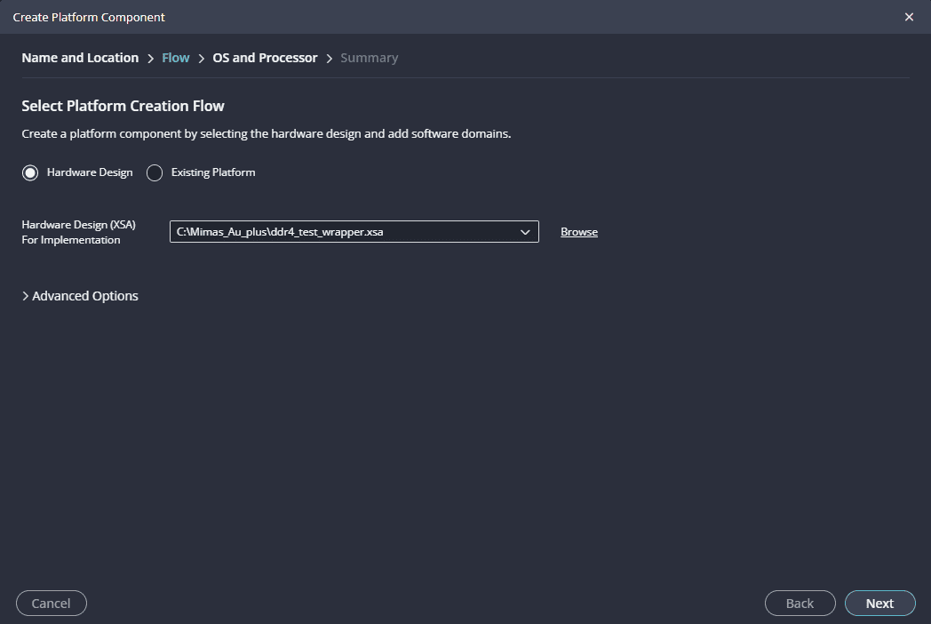
In the next tab browse the XSA file , select it , click on “Next”. In the next OS and Processor tab click “Next” and “Finish”.
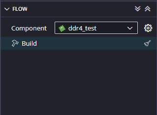
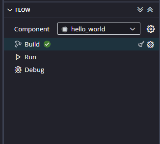
After successful creation of the platform, build the platform.
Step 17:
Next create the Memory Test Application component by selecting the “Memory Tests” template from the “examples”.
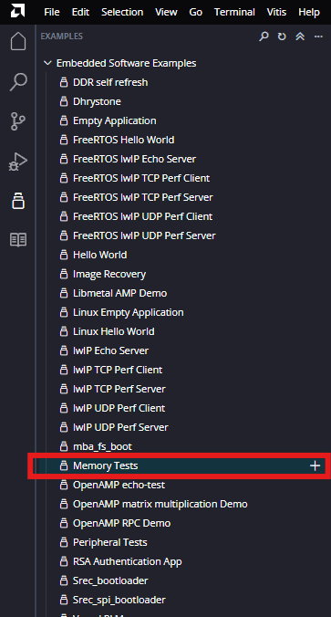
When the memory tests project is added successfully, build the project manually.
Step 18:
Once the build is completed successfully, power up Mimas AU plus FPGA Development Board using USB type C cable and connect the JTAG cable for programming the device.
Step 19:
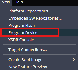
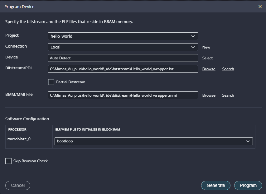
Program the FPGA on Mimas AU Plus with a simple boot loop program by selecting the Program Device option from the Vitis menu.
Once the “Program Device” window opens give the path for .bit and .mmi files .
If the “BMM/MMI” File is not selected , manually browse and select the file .Once the files are selected click on “Program” .
Step 20:
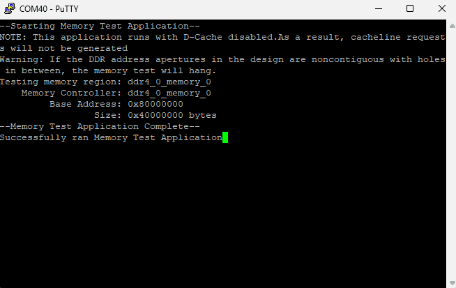
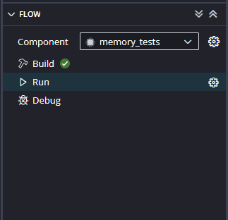
Meanwhile, open any serial terminal program (such as PuTTY, Teraterm etc) and open the port corresponding to Mimas AU plus with a 9600 baud rate (the default baud rate given in UART IP). Run the application by selecting the “Run”.
Step 21:
If everything went well, the Memory tests application running on the board should start printing the Memory tests over the UART and the output should be displayed on the Serial Terminal application as shown in the image below.