INTRODUCTION
This article aims to guide readers on how to effectively utilize the DDR3 memory available on the Spartan-7 FPGA using the AMD Memory Interface Generator (MIG) 7 IP Core. The MIG 7 IP core is a powerful tool provided by AMD that simplifies the process of interfacing with external DDR3 memory by handling the complex timing and calibration requirements.
When working with the MIG 7 IP core, users are presented with two interface options:
User Interface: This is a straightforward wrapper built on top of the Native Interface. It simplifies communication with the DDR3 memory by providing clear signal naming and intuitive data flow control. AXI4 Interface: This interface follows the AXI4 protocol, which is widely used in FPGA designs for memory-mapped transactions. It allows seamless integration with AXI-based designs, providing better scalability and compatibility with IP cores that utilize the AXI protocol. In this article, we’ll focus on how to test the DDR3 memory using the Memory Tests Template available in Vitis. This test template is a convenient way to verify memory functionality, ensuring that data can be reliably written to and read from the DDR3 memory. By following this guide, you’ll gain insights into configuring the MIG 7 IP core, integrating it into your Vivado design, and performing practical memory tests on the Spartan-7 FPGA.
Whether you’re a beginner or an experienced FPGA developer, this article will provide clear steps and explanations to help you successfully interface with DDR3 memory on the Spartan-7 platform.
Hardware required:
- Elbert S7 FPGA Development Board
- AMD Platform Cable USB II (JTAG cable)(optional)
- USB Type-A to Micro-C cable
- 5V DC power supply
Software required:
- Vivado Design Suite with Vitis installed (2024.1)
- Serial terminal application (PuTTY, Tera Term, etc.)
Creating MicroBlaze based Hardware Platform for Elbert S7
The following steps will walk you through the process of creating a new project with AMD Vivado and building a hardware platform with MicroBlaze soft processor using the Vivado IP integrator. Numato Lab’s Elbert S7 FPGA Development Board is used in this article but any compatible FPGA platform can be used with minor changes to the steps. Screenshots are added wherever possible to make the process easier for the reader.
Step 1:
Download and install the Vivado Board Support Package files for Elbert from here. Follow the README.md file on how to install Vivado board support files for Numato Lab boards.
Step 2:
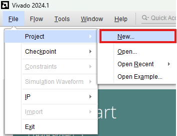
Open the AMD Vivado Design suite, go to “File -> Project -> New” to create a new project. The “New project” window will pop up. Click “Next”.
Step 3:
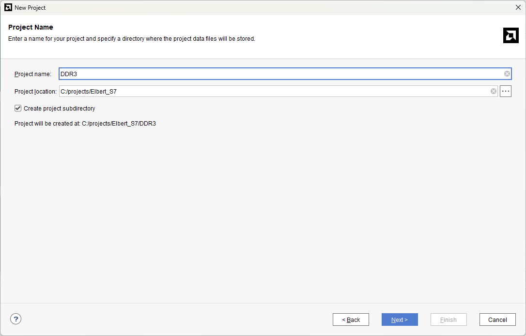
In the “Project Name” window, enter a name for the project and save it at a suitable location. Select the option “Create project subdirectory” to keep all the project files in a single folder. For this example, “DDR3” is used as the project name, but feel free to use any name. Click “Next”.
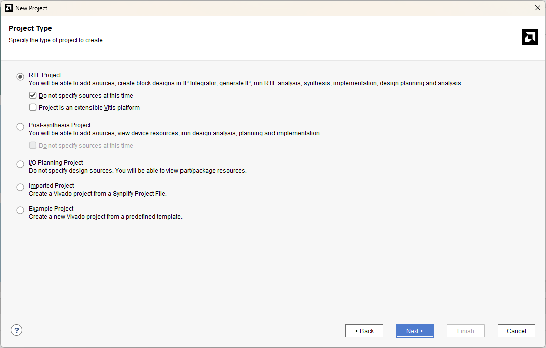
Now you will see the “Project Type” page as shown below. Select the “RTL Project” and select the option “Do not specify sources at this time”. Click “Next”.
Step 4:
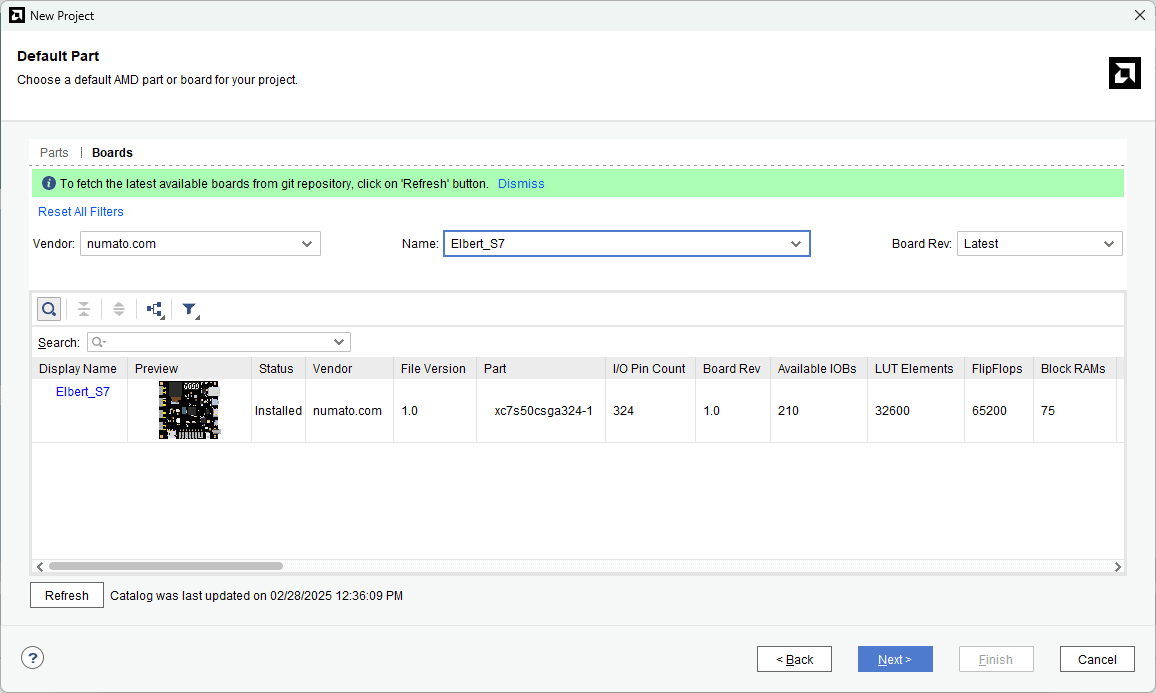
In the “Default Part” window, select the “Boards” tab. Choose the Vendor as “numato.com”, filter the Name “Elbert” and select the board as shown below. Click “Next” to continue. If Elbert is not displayed in the boards list, make sure that the board support files are installed correctly.
In the next window, click “Finish” to complete creating the new project. When the new project wizard exits, a new project will be created by Vivado with the specified settings.
Step 5:
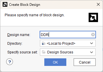
Under the “Flow Navigator” panel, click “Create Block Design” under the IP Integrator section. Enter a name for the block design and click “OK”. An empty block design will be created.
Step 6:
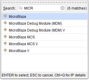
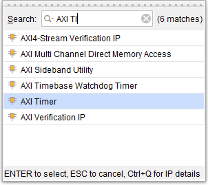
In the Diagram window, right-click and select “Add IP” from the popup menu. Search for “MicroBlaze” & “AXI Timer” and add them to the design by double-clicking them.
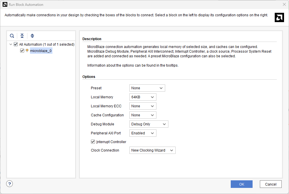
Step 7:
Click “Run Block Automation” present in the “Designer Assistance available” bar on the top left corner of the window to complete the design. Select the settings as shown in the following image.
Step 8:
Click the “Board” tab. The default peripherals available for the Elbert board will be listed as shown below.
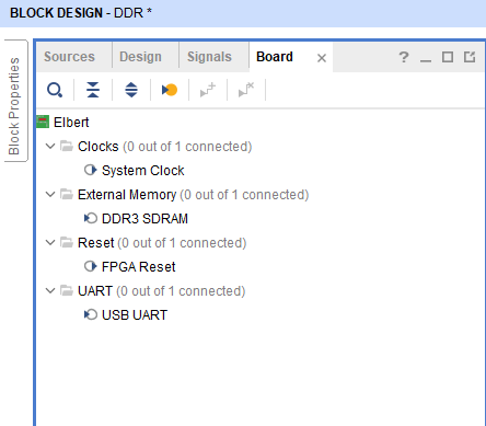
Add DDR3 SDRAM and USB UART to the design by double-clicking the corresponding peripherals.
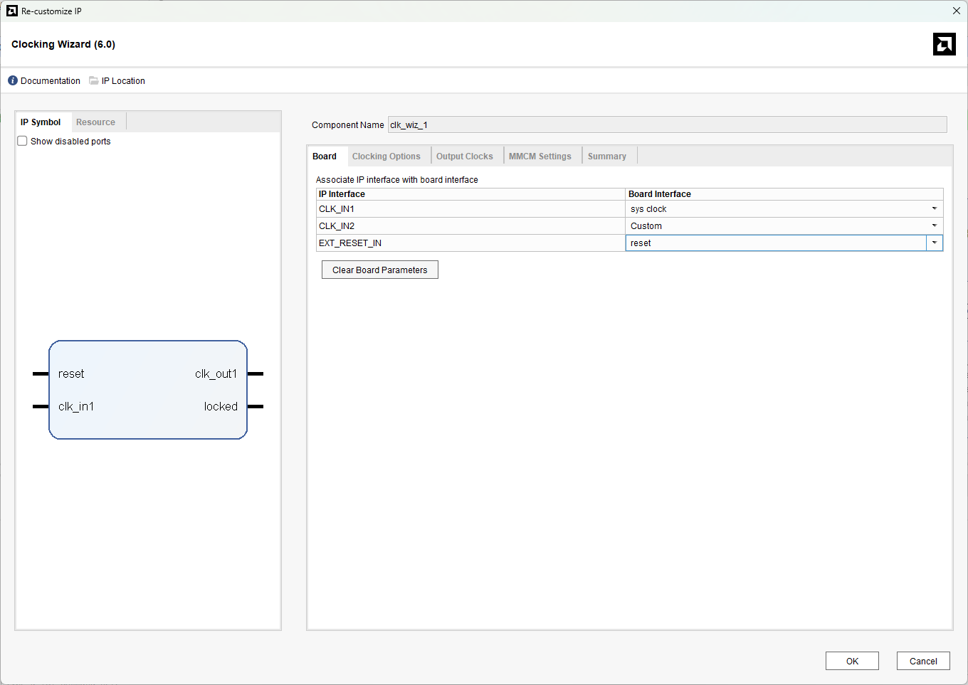
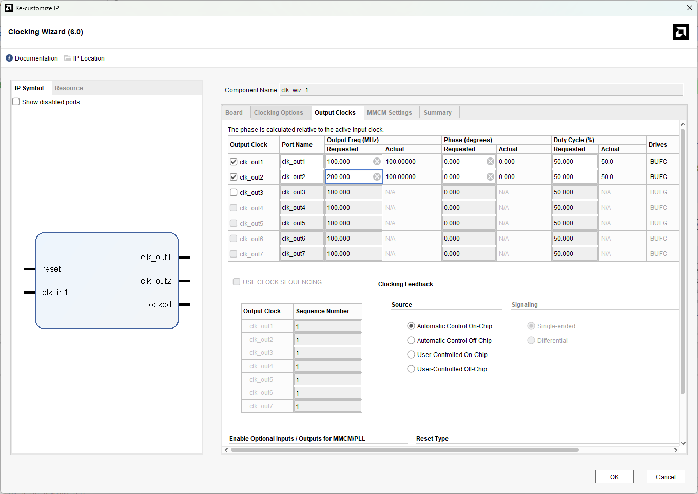
Step 9:
Double-click on the “Clocking Wizard” IP block and change the settings as shown below. In the “Output Clocks” section, set clk_out1 frequency to 100 MHz and clk_out2 to 200 MHz.
Step 10:
Remove the existing connection to sys_clk_i of the “MIG 7 Series” block and connect it to clk_out2.
Step 11:
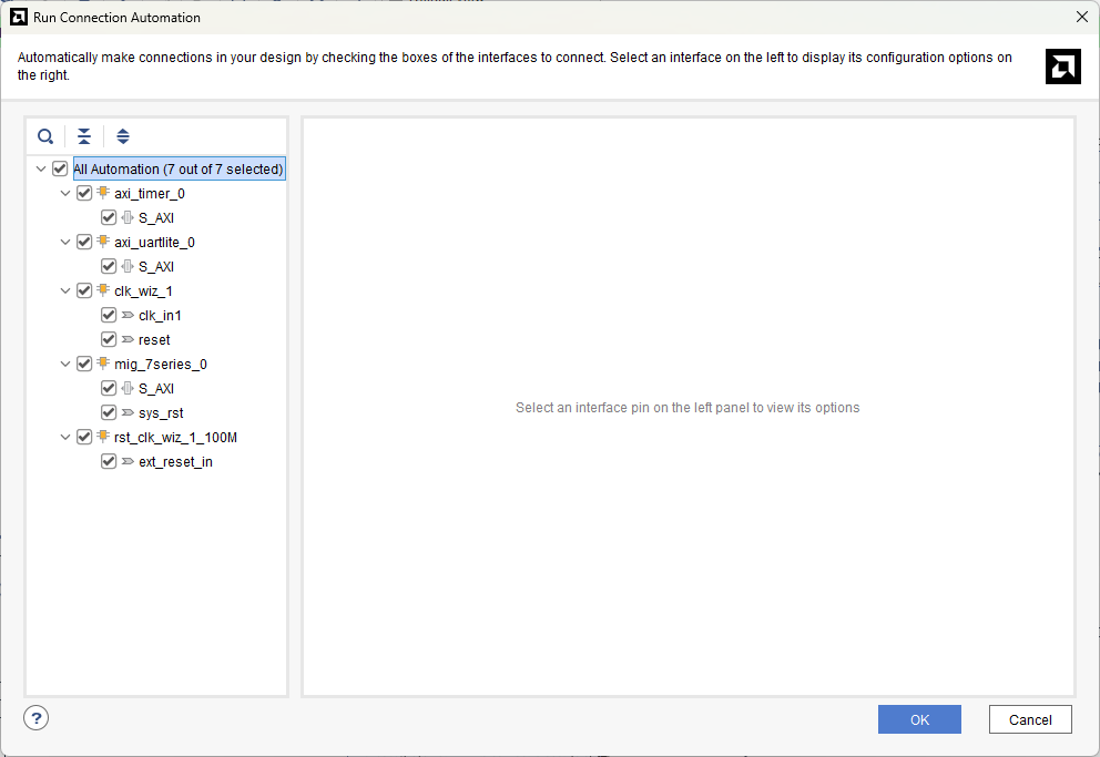
Run “Connection Automation” so Vivado can connect the blocks to make a complete system.
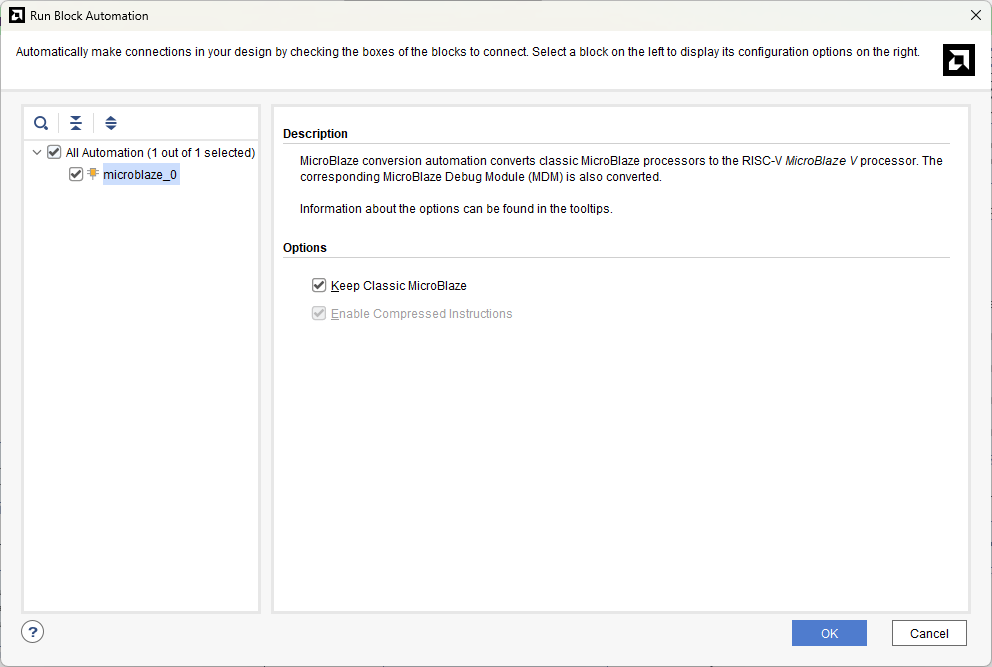
Click on “Run Block Automation” and select keep Classic Microblaze option as shown in the picture below.
Step 12:
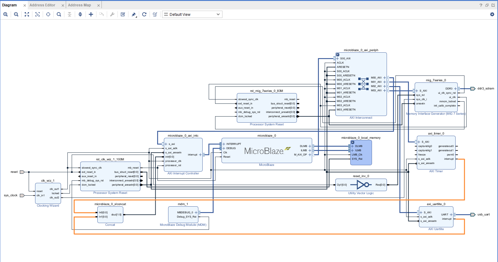
Connect interrupt output lines from “AXI Timer” and “UARTLite” to the “Concat” block as shown below figure. Select the “Validate Design” option from the Tools menu to make sure that connections are correct.
Step 13:
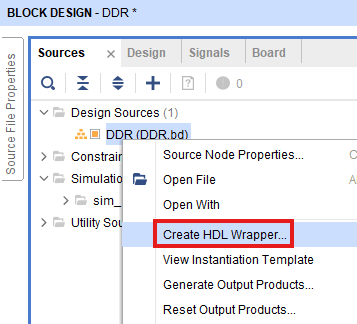
Right-click “ddr3” in the “Sources” window, and select “Create HDL Wrapper” from the popup menu. Click “OK” on the window that appears to finish generating a wrapper
Step 14:
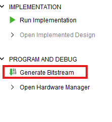
Click “Generate Bitstream” under the “Program And Debug” section to synthesize, implement and generate a bitstream.
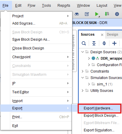
Step 15:
After generating the bitstream successfully, select Export -> Export Hardware from the File menu. Click Next.
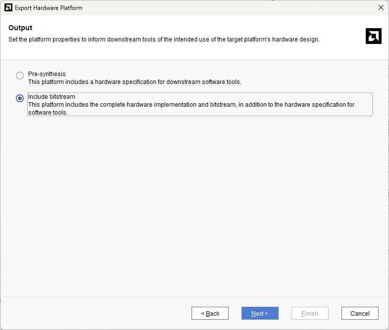
Select the “include bitstream” checkbox and click Next.
Step 16:
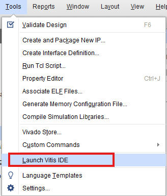
Select Launch Vitis IDE from the Tools menu.
Step 17:
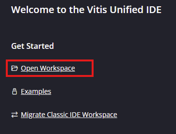
After Vitis Unified IDE window opens, click on “Open Workspace” and select necessary folder to keep the Vitis files.
Step 18:
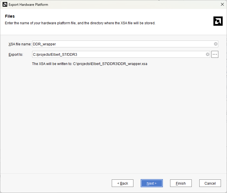
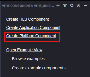
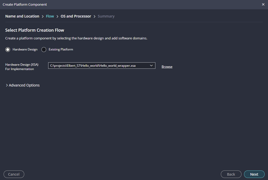
Create a new platform for the project, by selecting “Create Platform Component”, click “Next”, in the Flow tab select the XSA file saved using the step 15 and finally click “Next” and “Finish” respectively.
After successful creation of the platform, build the platform.
Step 19:
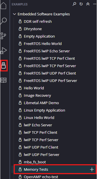
Next create the DDR3_test Application component by selecting the “Memory tests” template from the “examples”,
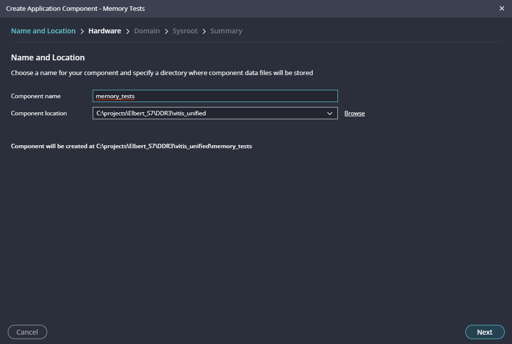
In “Create Application Component” tab specify project name and location, click “Next”
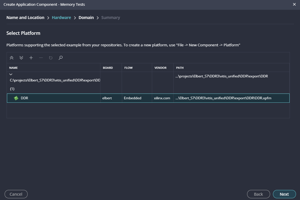
Select newly created Platform and click “Next”.
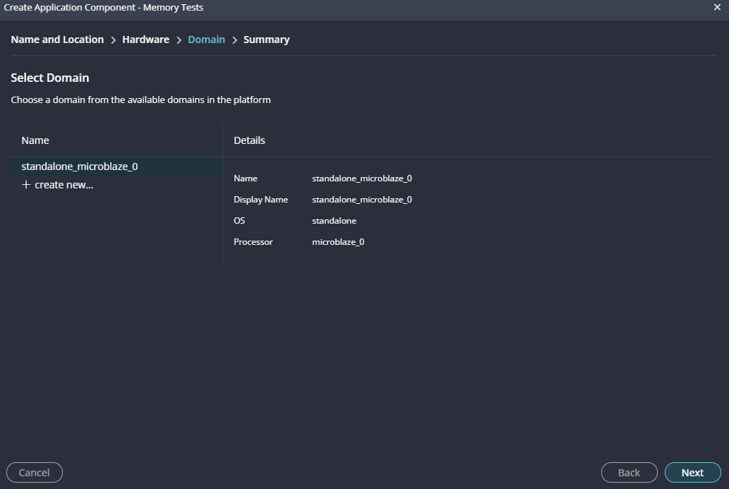
Select the domain as “Standalone_microblaze_0” and click “Next” and click on “Finish”
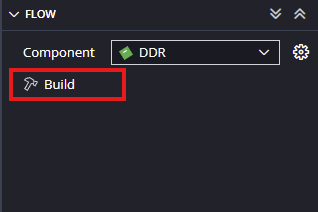
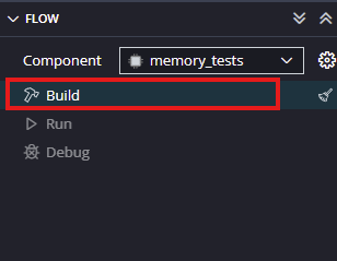
When the Memory tests project is added successfully, build the project manually.
Step 20:
Once the build is completed successfully, power up Elbert S7 using an USB type C cable.
Step 21:
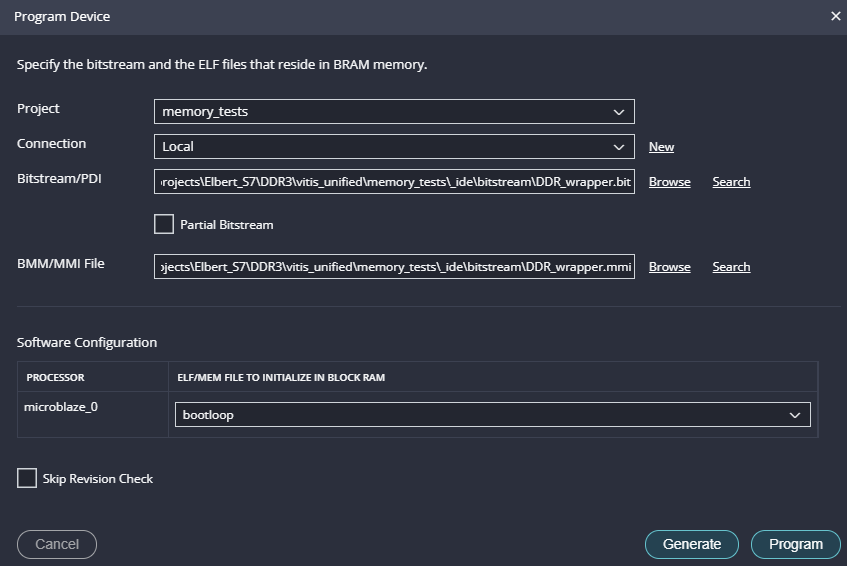
Program the FPGA on Elbert S7 with a simple boot loop program by selecting the Program Device option from the Vitis menu.

Once the “Program Device” window opens click on “Program“.
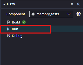
Step 22:
Meanwhile, open any serial terminal program (such as PuTTY, Teraterm etc) and open the port corresponding to Elbert S7 with a 9600 baud rate (the default baud rate given in UART IP). Program the board by selecting the “Run”.
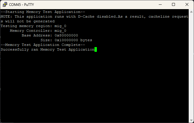
Step 23:
If everything went well, the application running on the board should print the memory testing Process over the UART and should be displayed on the Serial Terminal application.