Introduction
Testing DDR3 DRAM on an FPGA involves checking the performance and reliability of dynamic random-access memory (DRAM) modules within a FPGA. This process ensures that the DRAM interacts correctly with the FPGA, verifying that data is stored and retrieved accurately under various conditions. Effective testing is crucial for optimizing memory systems and enhancing overall system performance. The Purpose of this article is to help readers to understand how to test DRAM memory available on Styx using Zynq DRAM tests template.
Styx Z7 FPGA Module
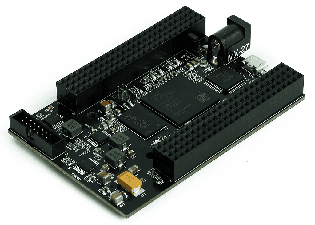 Styx Z7 FPGA Module is the first product from Numato Lab featuring Zynq-70xx SoC. Styx is pin-compatible with Numato Lab’s Saturn Spartan 6 FPGA module, Neso Artix 7 FPGA module and Skoll Kintex 7 FPGA module and allows for seamless upgrade in most cases. Styx offers built in USB 2.0 interface that can be used to program the board as well as do debugging or data transfer with the host.
Styx Z7 FPGA Module features a Zynq 7020 from Xilinx in CLG484 package. The unique feature of Zynq-7000 series is that they are complete System on Chip (SoC) with an FPGA die which makes it a very powerful combination. Zynq 7020 has dual-core ARM Cortex A9 and a whole bunch of peripherals which are typically found in SoCs. Additionally, it has Artix-7 equivalent programmable logic section, connected to SoC using AXI interconnects. This SoC + FPGA combination makes Zynq very flexible for multitude of uses. With Zynq 7020 on board, Styx is a great choice for learning, product development and OEM integration.
Prerequisites
To follow this article, you would need the following:
- Hardware:
- Styx Z7 FPGA Module
- Xilinx Platform Cable II JTAG debugger.
- Software:
- Xilinx Vivado Design Suite 2024.1
- Vitis 2024.1
- FT_Prog tool for configuring on-board FT2232H USB Serial converter (download and install from FTDI website)
Let’s get started
The following steps will walk you through the process of creating a new project with Vivado and building a hardware platform with Zynq processing system using IP integrator. This article is written for Numato Lab’s Styx Zynq Module, but can be adapted to any other Zynq based platform with minor changes. Screenshots are added wherever possible to make the process easier to the reader.
Step 1:
Download and install Vivado Board Support Package files for Styx from here. Follow the readme in the link on how to install Vivado Board Support Package files for Numato Lab’s boards.
Step 2:
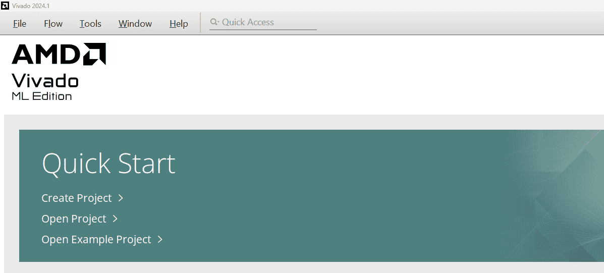
Start Vivado Design Suite, and select “Create New Project” from Quick Start section. The project wizard will pop up. Press next to proceed with creating the project.
Step 3:
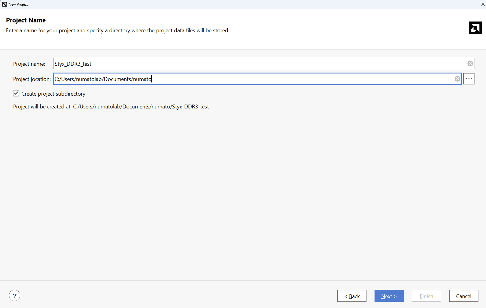
Type in a project name and save it at a convenient location. For this example “Styx_DDR3_test” is used as project name, but feel free to use any name. Select the check box below to keep all project files in a single folder. The image below shows the settings for the example project. Click “Next” to continue.
Step 4:
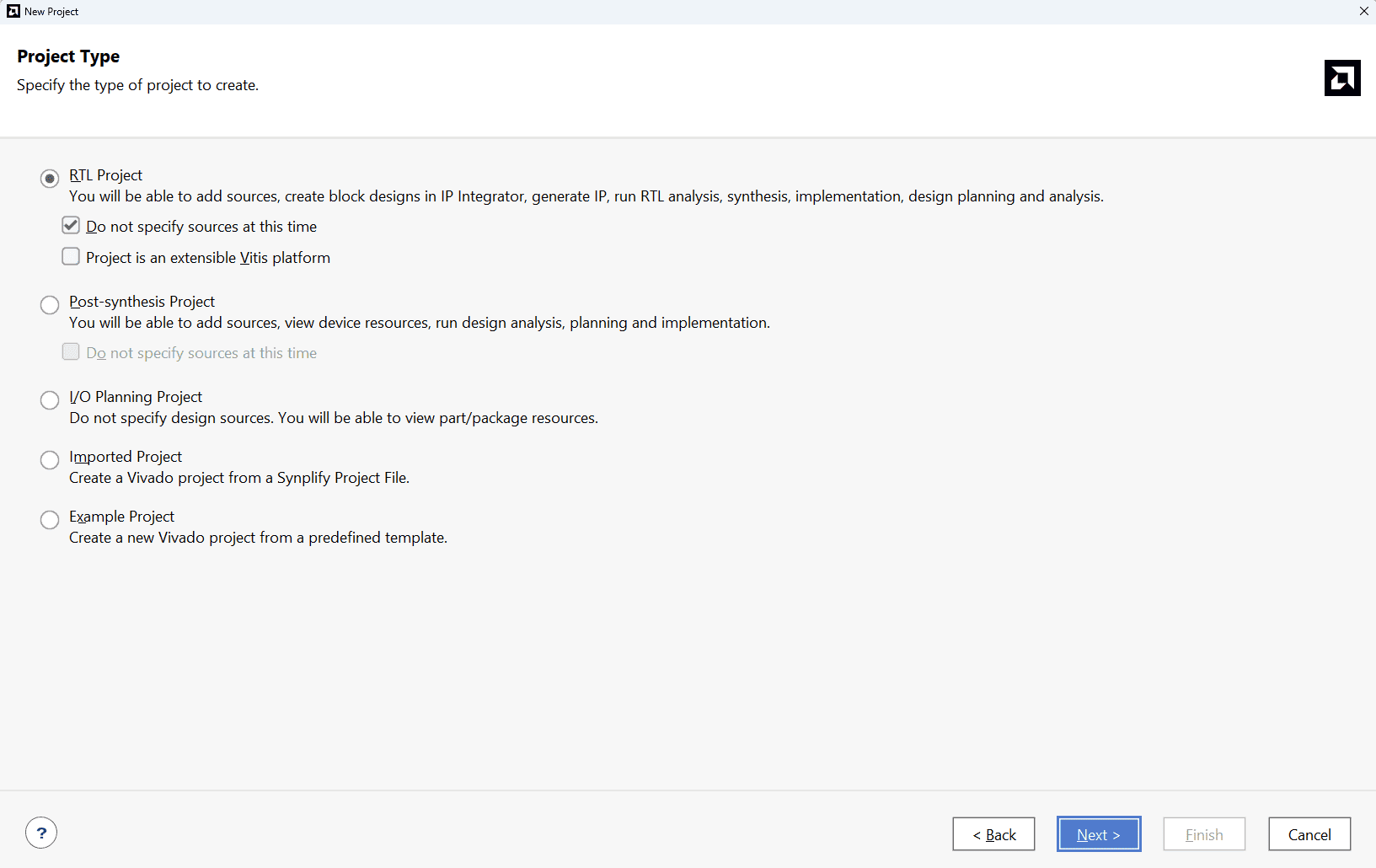
Choose “RTL Project” as project type and check the option “Do not specify sources at this time”.

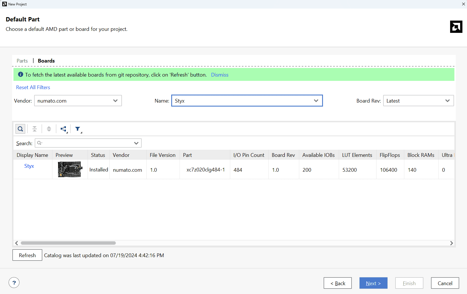
Step 5:
At the “Default Part” step, select “Boards” and choose Vendor as “numato.com”. Select “Styx” and click “Next”. If Styx is not displayed in the boards list, you will need to install Styx board support files correctly.
Continue the wizard and finish creating the project. When the new project wizard exits, a new project will be opened up in Vivado with the settings you have selected.
Step 6:
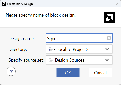
Under Flow Navigator, select “Create Block Design” in IP Integrator. Give an appropriate name to design. We will call it “styx” for example.
Step 7:
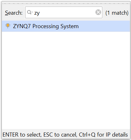
Go to Diagram window, right click and select “Add IP” from the popup menu. Search for ZYNQ7 Processing System. Add it to block design by double clicking.
Step 8:
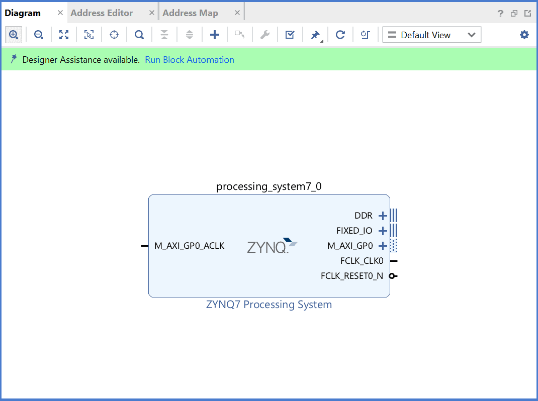
Click on “Run Block Automation” option on the green bar.
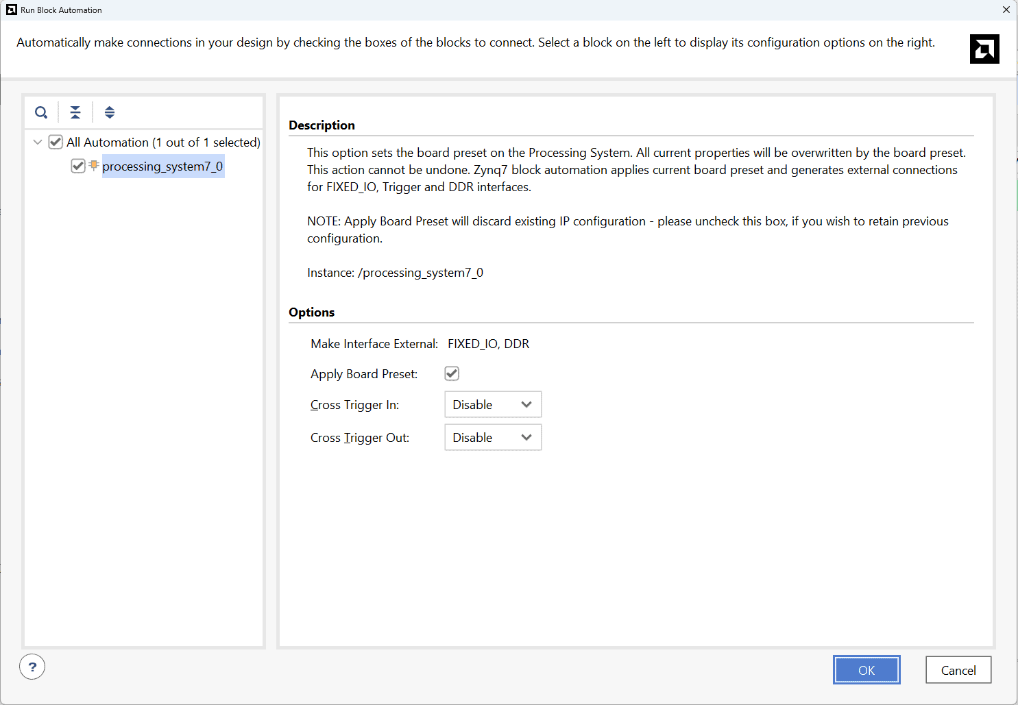
Step 9:
In the “Run Block Automation” window, select the options as in image below and click OK.
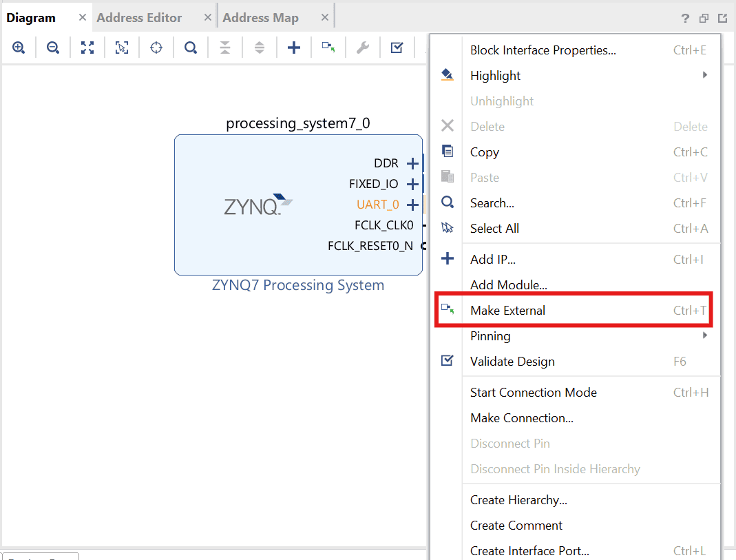
Step 10:
The Zynq IP block will have changed after running block automation. Right click on “UART_0” port of the Zynq IP block and select “Make External”.
Step 11:
Now we have to add constraints for the external UART_0 port. In the Sources window, right-click anywhere and select “Edit Constraints Sets”. Add a new constraints file, paste the code below and save the file with a convenient name.
set_property -dict {PACKAGE_PIN T22 IOSTANDARD LVCMOS33} [get_ports UART_0_0_rxd]
set_property -dict {PACKAGE_PIN T21 IOSTANDARD LVCMOS33} [get_ports UART_0_0_txd]
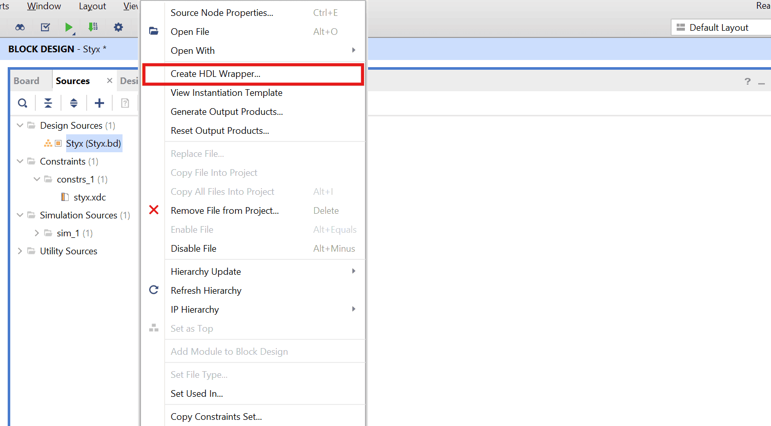
Step 12:
Go to “Sources” tab, right click on “styx” design file and select “Create HDL Wrapper”. Click OK on the window that appears to finish generating wrapper.
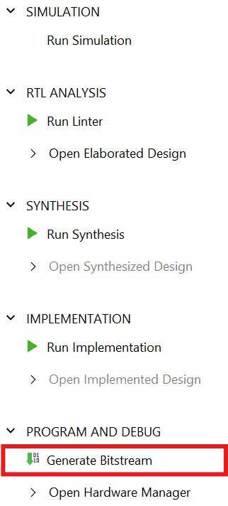
Step 13:
Click “Generate Bitstream” under PROGRAM AND DEBUG section and click “Yes” in any subsequent dialog window which comes up.
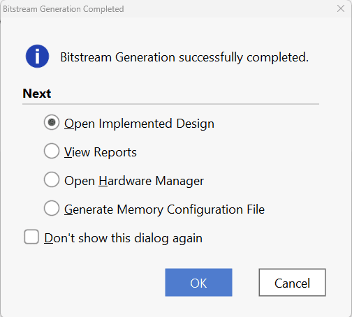
Step 14:
Once the bitstream is successfully generated, close any “Bitstream Generation Completed” dialog which comes up asking for what to do next.
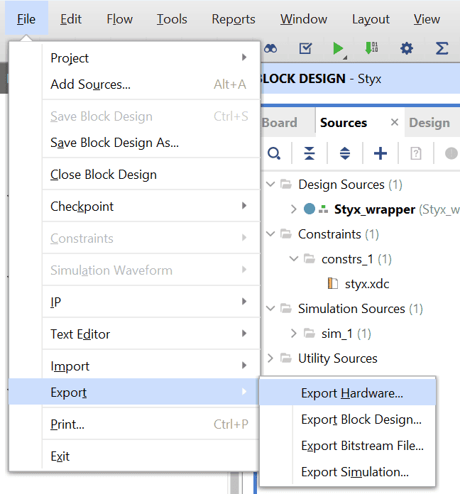
Go to File -> Export -> Export Hardware…
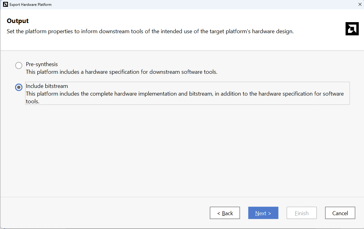
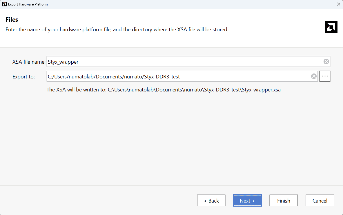
Check “Include bitstream”, keep “Export to:” default, and click OK.
Step 15:
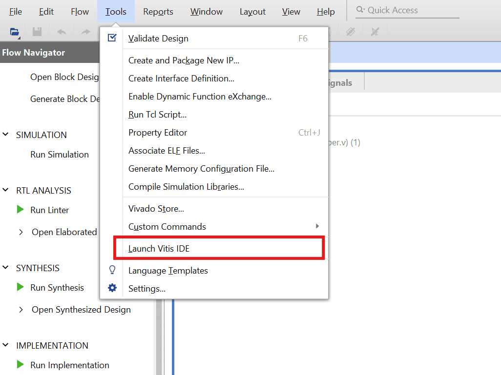
Finally open Vitis unified IDE by following the steps Tools–> Launch Vitis IDE .
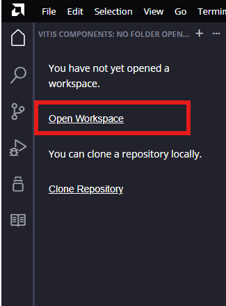
Step 16:
After Vitis windows opens, click on “Open Workspace” and select necessary folder to keep the Vitis files.
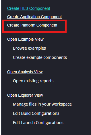
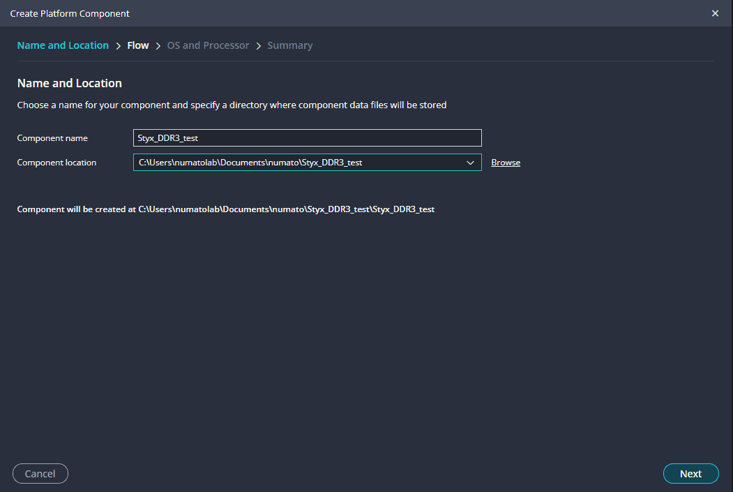
Step 17:
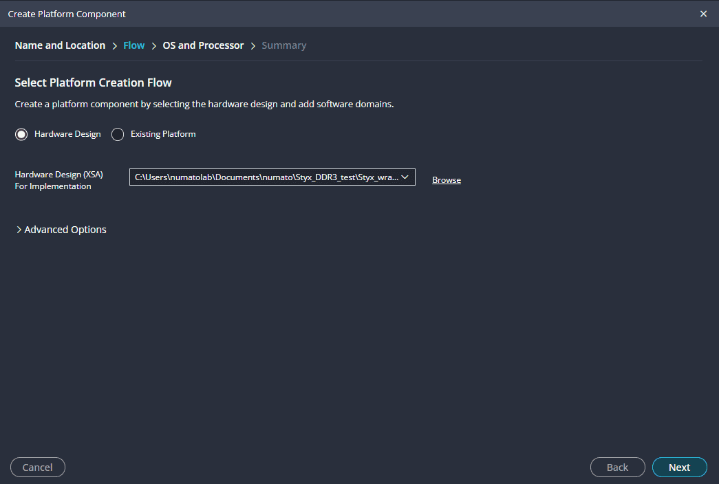
Create a new platform for the project, by selecting “Create Platform Component”, click “Next”, in the Flow tab select the XSA file saved using the step 14 and finally click “Next” and “Finish” respectively.
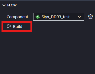
After Successful creation of the platform, build the platform.
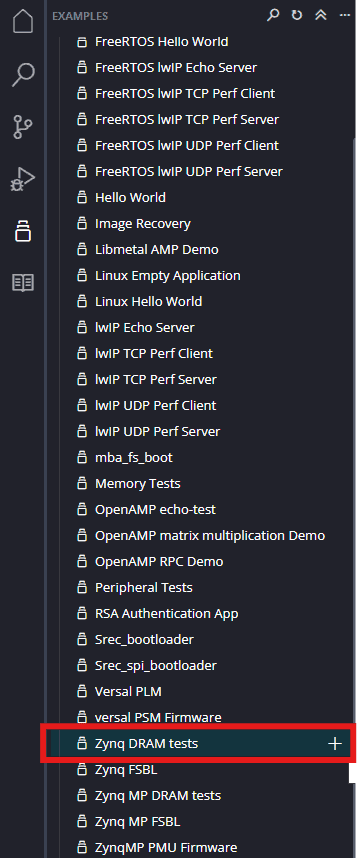
Step 18:
Next create the Zynq DRAM tests Application component by selecting the “Zynq DRAM tests” template from the “examples”, select “Create Application Component from Template”, specify project name and location, click “Next”, select newly created platform, click “Next” and then finally “Finish”.
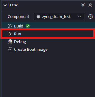
When the Zynq DRAM tests project is added successfully, build the project manually.
Step 19:
Once the build is complete successfully, power up Styx Zynq Module and connect Xilinx Platform USB cable and Micro USB cable for Serial debugging to the board. Make sure to configure channel A of the onboard FT2232H USB – Serial device as virtual communication using FT_Prog. The process is very similar to that of Saturn and details are available here. Change the Styx’s Boot Mode to JTAG. Please refer to user manual to learn more about configuring Styx’s Boot Mode.
Step 20:
Meanwhile, open any serial terminal program (such as PuTTY, Teraterm etc) and open the port corresponding to Styx’s Channel A at 115200 baudrate. Program the board by selecting the “Run”.
Step 21:
If everything went well, the Zynq DRAM tests application running on the board should start printing the Zynq DRAM tests over the UART and the output should be displayed on the Serial Terminal application as shown in the image below.
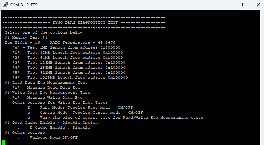
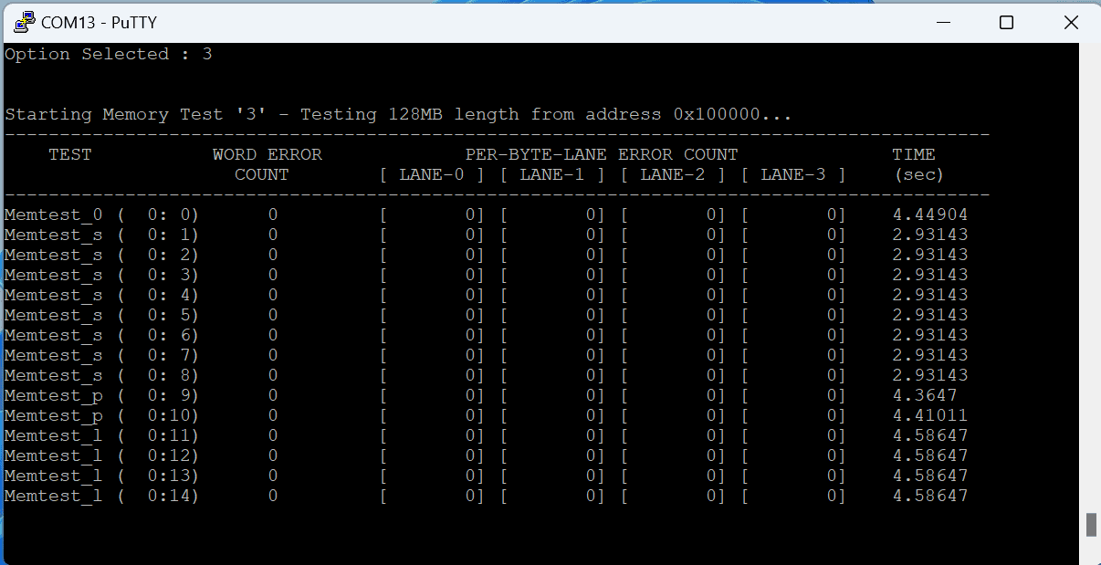
Here we are testing for 128MB(option:3) , we can test till 1023MB by selecting respective options in the serial terminal.