Selection of an FPGA part for any project is one of the most crucial decisions during the project planning stage which has long-term implications on the project. More often than not, it is an optimization problem, where the project requirements decide the trade-offs and compromises between features and capabilities. There are a myriad of FPGA features which need to be considered during the planning and decision stage.
Let’s discuss the common FPGA features one by one.
FPGA Package
FPGA Package refers to how the FPGA pins are brought outside the FPGA, i.e, the packaging of the FPGA. The PCB footprint of FPGA package is a 2D rendering of the surface where FPGA comes in contact with the PCB. Just like common microcontrollers are available in packages such as DIP, SOIC, QFP, etc. Similarly, FPGAs are available in different packages. FPGA Manufacturers provide a detailed drawing of the PCB footprints of any FPGA package. FPGAs vary widely in package types available to the customer.
FPGA package is a deciding factor in:
- Number of I/Os in an FPGA chip
- Number of Multi-Gigabit Transceivers (MGT)
- Maximum speed of the I/Os and MGTs in an FPGA chip
- PCB routing rules, guidelines, and constraints
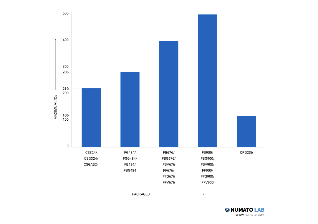
Maximum I/Os vs packages. See the source for more details. (https://www.xilinx.com/support/documentation/selection-guides/7-series-product-selection-guide.pdf)
There are FPGAs available in as little as 25-pins WLCSP package with 20 I/Os to staggering 2892-pins BGA packages with ~800 I/Os. A lot of applications require as high number of I/Os as possible. These applications could be as simple as driving a huge number of LEDs to as complex as controlling hundreds of motors for robotics or industrials applications. The number of I/Os needed is decided by the project, and this, in turn, narrows down the package options.
The next important consideration is the PCB layout constraints. Is the project meant for really compact end-user devices such as smartphones or is it meant for rugged industrial and military equipment? In the first scenario, the package should be as small as possible with an extremely fine pitch between pins. Whereas in the latter case, the design constraints can be relaxed to accommodate a very big FPGA with greater ball pitch. The package decision subsequently affects many aspects of the project such as mechanical dimensions, PCB layer stack-up, PCB routing, and manufacturing constraints, limits on Multi-Gigabit Transceiver (MGT) speeds, etc. For hobbyists, the BGA and WLCSP types of packages can be difficult, instead QFP package FPGAs might be better preference. Companies with advanced PCB assembly machines would definitely prefer BGAs. In the category of BGAs, there are packages such as Wire-Bond BGA which offer lower MGT speeds compared to others such as Flip-Chip BGA.
Most FPGA manufacturers offer a feature known as “Device Migration”. This means that if you select any FPGA with a particular package, there might be options available to upgrade to a higher-end FPGA in the same package. Taking the example of Xilinx Artix-7 FPGA family illustrated in the image below, if you select XC7A50T for example in an FGG484 package, then you have 5 more Artix-7 devices with same compatible footprint, and you can choose to upgrade to a higher-end FPGA or downgrade to a lower-cost, lower-end FPGA and keep your hardware design same. This feature provides mobility and flexibility in terms of cost and optimal FPGA utilization.
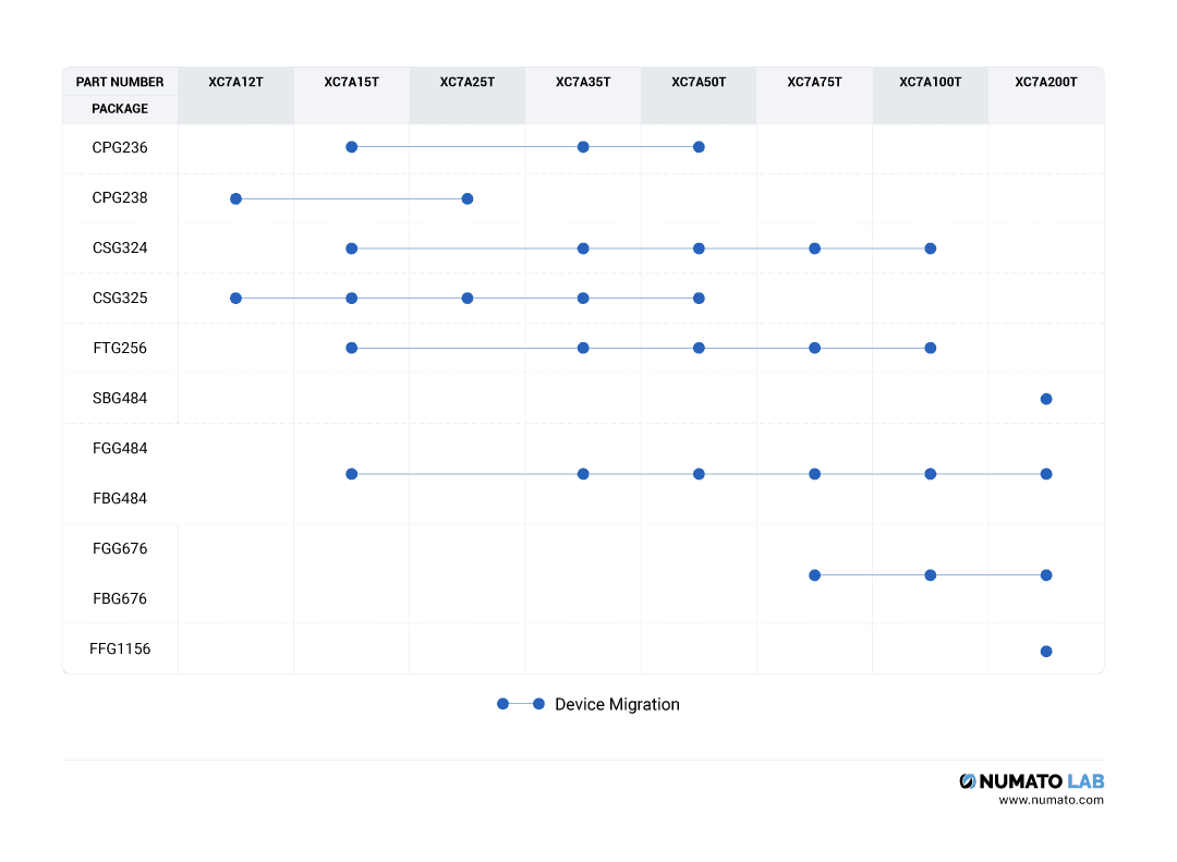
Table: Device migration and footprint compatibility between Artix-7 FPGAs. See Source for details. (https://www.xilinx.com/support/documentation/selection-guides/7-series-product-selection-guide.pdf)
FPGA Resources
The optimal amount of FPGA resources required, and additionally, the kind of FPGA resources required is dependent on project requirements. Some projects may require a high number of I/Os whereas some projects may just need the DSP slices of an FPGAs. Following are the major FPGA resources:
- Logic resources (LUTs, Flip-Flop, etc)
- Memory resources (Distributed RAM, Block RAM, etc)
- Clock resources (PLL, MMCM, etc)
- I/Os (Single-ended and differential)
- DSP slices
- Hard-blocks such as ARM cores, PCIe, 100G Ethernet, Interlaken, etc
- MGT Transceivers
The previous section on FPGA packaging shed some light on I/Os and MGT transceivers as part of packaging since they strongly decide the FPGA package and pin-count. In Xilinx jargon, MGTs are referred by one of the following possible names depending on their maximum transmission rates: GTP, GTX, GTH, GTM, GTY, and GTZ. These are all multi-gigabit transceivers but their speed capabilities vary. DisplayPort typically needs only four transceivers, but PCI Express may need up to 16 transceivers. This number is dependent on the target application.
Nereid/Proteus vs Elbert V2 (comparison table):
| FPGA Board | Kintex 7 in Nereid & Proteus | Spartan 3A in Elbert V2 |
|---|---|---|
| FPGA | XC7K410T FPGA with 400K logic cells | XC3S50A containing roughly 1600 logic cells |
| Memory | Up to 35 Mb on-chip memory | On-chip memory less than 100 Kb |
| Other Resources | Multi-Gigabit Transceivers (MGTs), DSP Slices, support for Gigabit Ethernet | No transceivers or DSP |
It is not recommended to shortlist an FPGA which has almost the same amount of logic, memory or clock resources as the design requirement. Place & Route tools start to struggle once the FPGA starts getting saturated, and it will be difficult to achieve timing closure. So, it is recommended to budget for extra resources, maybe 20% to 30% more than actual design requirements.
Some FPGAs have dedicated hard-blocks for specialized purposes such as Memory Controllers, PCI Express hard-block and CPU cores (Power, ARM, RISC-V, etc). It is up to the project planners to figure out whether they require any dedicated hard blocks or not. It is also worth noting that FPGA cost will increase with the increase in the number of FPGA resources. Capabilities of resources also vary with newer FPGA architectures.
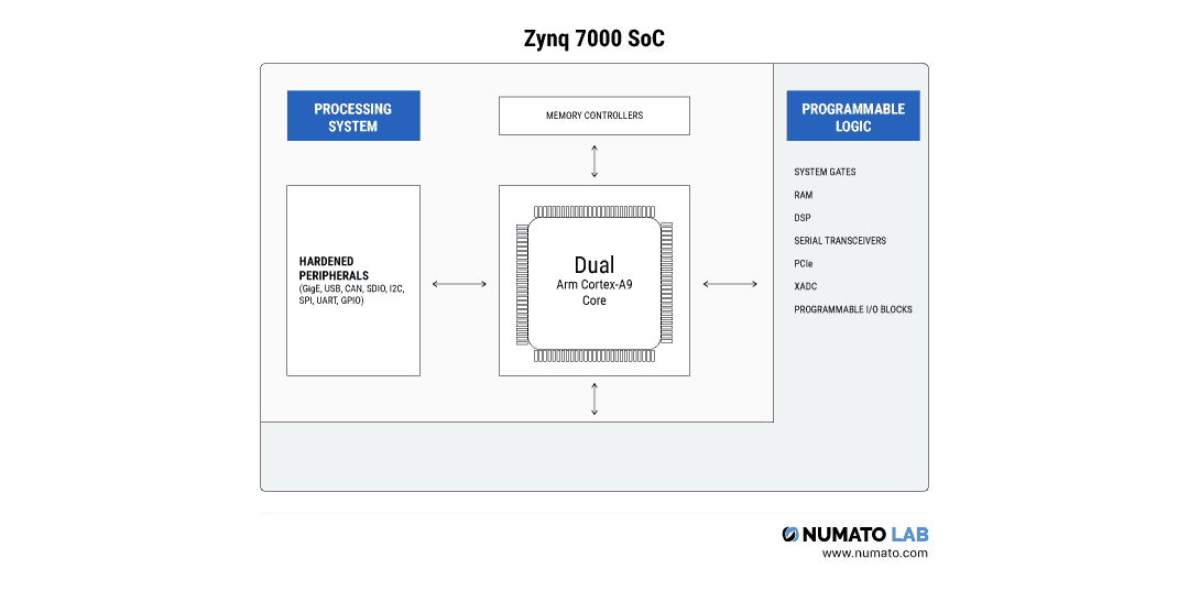
The Styx module features Xilinx Zynq XC7Z020 chip which integrates a hard-silicon ARM System on Chip (SoC) with Artix-7 based programmable logic. The SoC part of Zynq consists of
- Dual-core ARM Cortex-A9 Processors
- Hardened peripherals like Dual Gigabit Ethernet, SDIO, UART, SPI, I2C, etc
- Static and Dynamic Memory controllers and many other peripherals
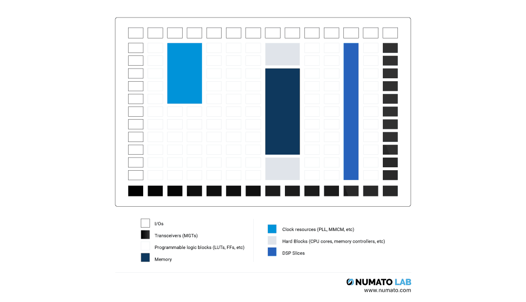
The block diagram below illustrates the Programmable Logic section and SoC (Processing System) section of Zynq:
The Telesto module features Intel MAX 10 FPGA which is a non-volatile programmable logic device. MAX 10 FPGA comes with on-die dual configuration NOR flash that allows very fast device configuration compared to traditional FPGAs.
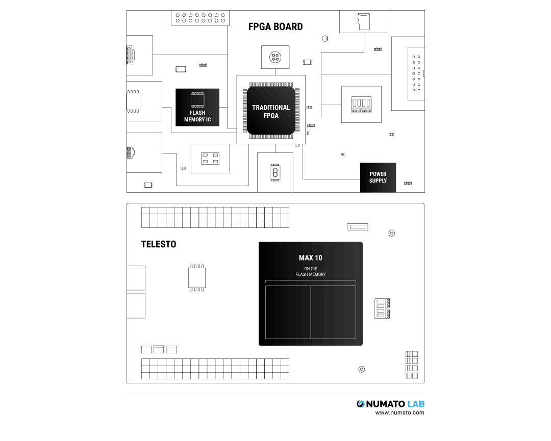
Unlike traditional FPGAs, there is no need for external configuration memory for MAX 10 based Telesto. This saves PCB design cost and the designs will be less prone to failure. Also, the dual configuration flash memory allows users to store and dynamically switch between two bitstreams on a single chip.
Interfaces
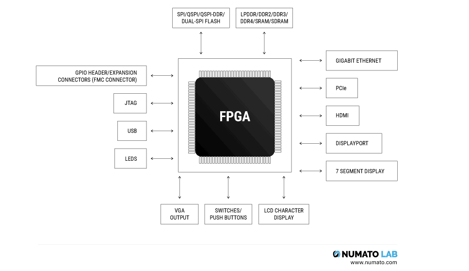
Almost all the communication with FPGA happens either through the available General Purpose Input Output or through specialized IOs like transceivers. If the design requires, for example, HDMI Input/Output then an FPGA which supports TMDS signaling should be considered. If the design needs DisplayPort or PCI Express etc, then an FPGA with MGT transceivers should be considered. Memories such as DDR2 and DDR3 require specialized I/O standards and features such as IODELAY.
The programming, debug and configuration interface typically consists of JTAG and a non-volatile memory for configuration bitstream storage. For remote system upgrade requirements, it might be better to select an FPGA with “Multiboot” or similar feature. It is not mandatory though, for example, if the FPGA configuration is controlled by a processor. Multiboot means FPGA can boot from one of the many images present in the non-volatile storage, and if it failed to boot from the upgraded images, then it can fall back to the “golden” bitstream.
Power Usage
FPGA are comparatively more power hungry than their ASIC counterparts. Power budgeting is very critical for power sensitive designs such as smartphones or the Internet of Things (IoT) devices. Newer generations FPGA family manufactured with denser process nodes such as 28nm or 14nm have lower power requirements per logic cell.
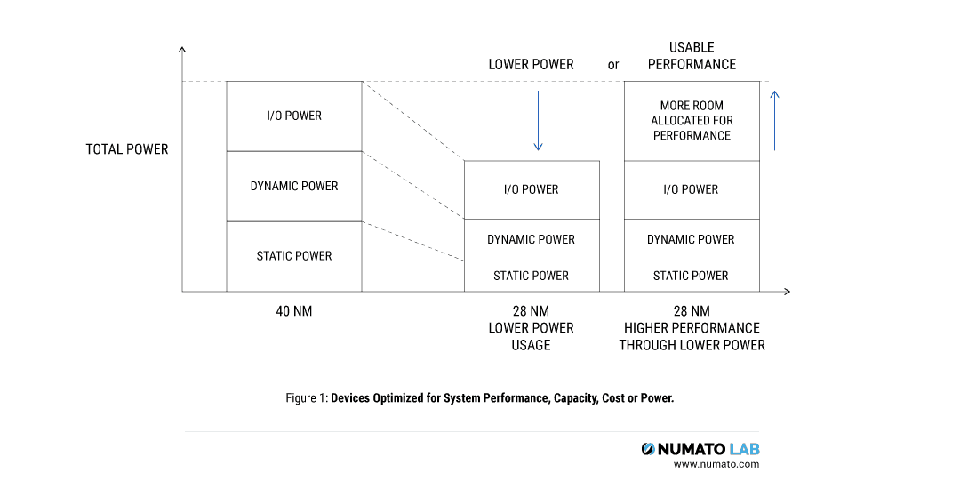
Even with power-efficient silicon processes, the huge FPGAs put heavy demands on the power supplies. Just the FPGA internal core itself may consume tens of amperes current. Add to that the power supplies for I/O, transceivers, block RAM, etc, the challenges increase manifold. Power supply vendors and FPGA vendors provide tools for power analysis for all FPGAs. We absolutely recommend using them for planning the power requirements of projects.
Cost
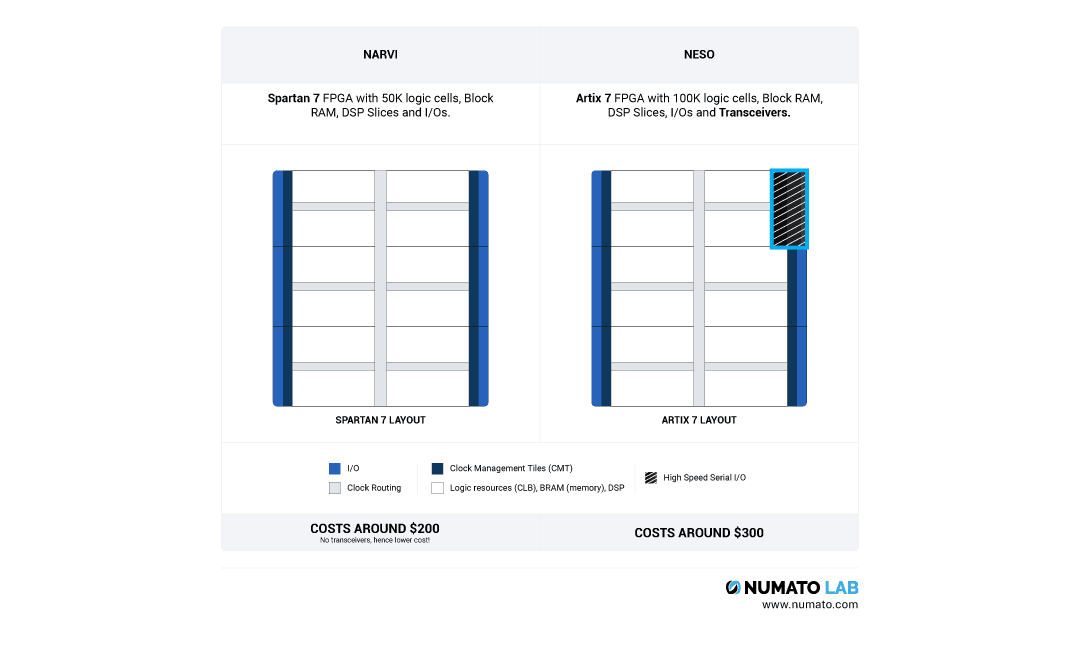
One last factor, albeit a major one, is cost. A simple rule is that any additional feature is going to increase the cost. Take the example of Spartan-7 vs Artix-7 FPGA families from Xilinx. The Spartan-7 series is very similar to the Artix-7 with the exception that there are no transceivers in Spartan-7 and that they are cheaper compared to Artix-7 counterparts for similar logic resource count. So, if you need an FPGA just for a large number of I/Os, it doesn’t make much sense to go with an FPGA which has transceivers which increase the cost, specially when you can get away with an identical FPGA at lower cost with required number of I/Os but doesn’t have transceivers. This was also one reason why Xilinx released Spartan-7 series. People complained that there are no options available to them without transceivers and they didn’t want to pay for the transceivers which they weren’t going to use. So, for this market segment, Spartan-7 makes more sense.
| Narvi | Neso |
|---|---|
| Spartan 7 FPGA with 50K logic cells, Block RAM, DSP Slices and I/Os. | Artix 7 FPGA with 100K logic cells, Block RAM, DSP Slices, I/Os and Transceivers. |
On the other side of the spectrum, the “heavy-weight”, higher-end FPGAs are super-expensive. But these FPGAs are targeted for the kind of applications where users are willing to pay for the expensive FPGAs because of their cutting-edge technologies and capabilities. For example, these FPGAs are used in top-of-the-line military Radars, next-generation wireless technologies, advanced digital signal processing, data center acceleration, etc. For these market segments, the cost is not a major deal-breaker. Instead, they are interested in staying at the frontier of technological prowess and capability, ahead of their competitors or adversaries.
How to select an FPGA board?
Selection of an FPGA board is very much influenced by the FPGA itself, but also by the overall board features and capabilities. We have already discussed the FPGA chip in the above sections. In this section, we will go into the thought process behind selecting any FPGA board.
Some non-exhaustive list of common factors which contribute in the decision process of selecting an FPGA board are: peripherals, expansion connectors, memory interfaces, ease of use, time to market, customization options, documentation, standards compliance and quality of support. Of course, the cost is also a factor.
Common Peripherals, Interfaces, Connectors, and Memories available in a typical FPGA Board
Peripherals
Peripherals along with expansion connectors are the distinguishing features of any FPGA board. Different target users have different expectations of which peripherals they want to see in an FPGA board. For example, students aspiring to learn about digital electronics and RTL designing would want peripherals such as switches, push-buttons, 7-segment displays, LEDs, USB-serial ports, LCD character display, VGA output, etc. They wouldn’t want higher-end peripherals simply because they are not yet at the stage where they can meaningfully use those peripherals. Elbert V2, Mimas V2, Waxwing Development Board and Mimas A7 FPGA Development board are examples of boards which cater to the expectations of the learner and hobbyist communities with a large number of learning-oriented peripherals.
Examples of the higher-end peripherals are Gigabit Ethernet, PCI Express, QSFP cages, USB 2.0/3.0 PHY, DisplayPort, etc. While these peripherals might not be of much use to any beginner, they are indispensable to a complex project which must necessarily use Gigabit Ethernet, for example, or any other peripheral due to project requirements. The Proteus Kintex-7 USB 3.0 FPGA Board, the Nereid Kintex-7 PCI Express development board and even Mimas A7 development board with Gigabit Ethernet and DisplayPort peripherals are some boards which fall in this category.
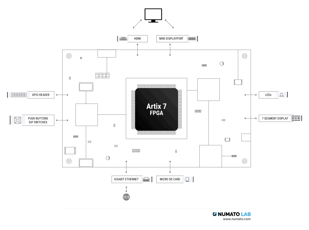
Peripherals in Mimas A7:
The table below highlights the contrast between a low-cost board, viz. ElbertV2 with limited, low-speed FPGA and peripherals, less number of GPIOs compared with high-end boards, viz. Nereid and Proteus, featuring technologically much more superior FPGA, higher-speed peripherals, connectivity options, transceivers and lots of GPIOs.
Nereid & Proteus Vs Elbert V2 :
| FPGA Board | Nereid & Proteus | Elbert V2 |
|---|---|---|
| FPGA User I/Os | Kintex 7 FMC HPC connector that provides maximum 174 I/Os | Spartan 3A Low-speed 0.1” connectors that provides maximum 39 I/Os |
| Other Peripherals/ Interfaces | Multi-Gigabit Transceivers (MGTs) on FMC HPC connector, PCIe interface (Nereid), 1 RGB LED, Micro SD card adapter, supports Gigabit Ethernet (requires expansion module) | VGA interface, Stereo Jack, LEDs, push buttons, DIP switches, Micro SD card adapter and 7-segment LED display |
For volume production, FPGA boards in module form-factor are also very popular. FPGA module boards are generally meant to be used with a carrier board to utilize their full potential. FPGA modules provide users with full flexibility in designing their own carrier boards with the peripherals, connectors, and hardware of their choice. For example, the Neso Artix-7 FPGA Module has been a very popular FPGA module due to module form-factor and additionally cross-compatibility with higher-end and lower-end modules in the same form-factor such as Narvi Spartan-7 Module, Skoll Kintex-7 Module, and Styx Zynq 7020 Module.
Connectors and Expansion I/Os Ports
While there is a large number of options for connectors, depending on desired speed and pin-count, it is best to prefer either standard connectors or use common, readily available ones so that users can design their own expansion modules easily. Connectors and Expansion I/O ports are terms used interchangeably in this context. Peripherals such as Ethernet, HDMI, etc have their own dedicated connectors but this paragraph refers only to the connectors or ports meant for I/O expansion.
Callisto K7 Vs Aller comparison in terms of I/Os:
| FPGA Board | Callisto K7 | Aller |
|---|---|---|
| FPGA | Kintex 7 | Artix 7 |
| User I/Os | 274 | No I/Os |
| Targeted Usage | Applications that require large number of I/Os | PCIe acceleration platform, Accelerated computing (hence no I/Os!) |
Connectors can be primarily classified into low-speed connectors vs high-speed connectors, and low-pin-count vs high-pin-count connectors. Pmod connectors are an example of low-speed, low pin-count connectors. They are very popular connectors amongst hobbyist targeted FPGA boards. The Elbert V2 and Mimas V2 have similar low-speed 0.1” connectors for expansion modules.
HDMI, SATA, and DisplayPort connectors are high-speed, low pin-count connectors. They are mostly used with their respective intended applications but can be used for custom applications also. In the other end of the spectrum are the high-speed, high pin-count connectors such as FMC (FPGA Mezzanine Card) connector, FMC+, HSMC (High-Speed Mezzanine Card) connector, VHDCI (Very High-Density Cable Interconnect) connector, PCI Express connector, etc. These connectors are mostly used in high-end FPGA boards which need to interface with high-sampling rate ADCs and high-speed DACs, multi-gigabit transceivers, etc. Signal integrity is the most important factor in these connectors. The Nereid Kintex-7 PCI Express FPGA development board has two high-speed connectors: PCI Express and FMC HPC (High Pin Count). The FMC connector in Nereid as well as in Proteus is VITA 57.1/ANSI compliant connector which means the complete ecosystem of compatible FMC expansion modules from various vendors can be used with both Nereid and Proteus without any major issues.
Onboard Memory Interfaces
Memory options in FPGA boards come in a wide range. Simplest being the SRAM and SDRAM. Other options are LPDDR, DDR2, DDR3, DDR4, etc. Depending on application and project requirements, even simple SRAM might suffice or higher capacity memories such as DDR3 and DDR4 might be needed. It is also important to factor in the availability of memory controller IP cores from the FPGA IC vendors or from third parties. For networking applications, memory technologies such as RLDRAM and QDR RAM are preferred due to low latency and high throughput respectively. SODIMM form-factor for DDR3 and DDR4 memory offers users with convenience to upgrade, downgrade or replace the memory modules anytime without any change in hardware. This makes SODIMM a very popular option amongst the users. The SODIMM memory modules are also comparatively cheaper and easily available off-the-shelf. The Nereid Kintex-7 PCI Express FPGA board features a SODIMM connector for DDR3L memories. The Proteus Kintex-7 FPGA Development board also has a SODIMM connector with exact same connections to FPGA as Nereid, hence making both compatible with each other. Other boards such as Neso, Narvi, etc have 2Gb DDR3 chip soldered into the module permanently. The Saturn Spartan 6 FPGA module has a 512Mb LPDDR chip onboard.
External RAM comparison: Nereid vs Saturn vs Neso:
| FPGA Board | Nereid | Saturn | Neso |
|---|---|---|---|
| FPGA | Kintex 7 | Spartan 6 | Artix 7 |
| Off-chip RAM | 4 GB DDR3L SODIMM SDRAM | 512Mb Mobile low-power DDR SDRAM (LPDDR) | 2 Gb DDR3 |
Apart from the volatile RAM memory, the other important memory to consider is the Flash Memory. It is especially important in case of FPGAs because the bitstreams for the designs running on FPGA are stored in this memory. During power-up, FPGA reads the bitstream from the flash memory and configures itself using this bitstream data. Flash memories with SPI communication interface are popular for this purpose and almost all FPGAs support configuring (or booting) themselves from SPI flash. Being a serial interface, with 1 bit-per-clock, the original SPI flash was found to be slow for the purpose of configuring big FPGAs. So, improved SPI interfaces such as Dual-SPI, Quad SPI (QSPI) and QSPI-DDR are used for faster data transfer. QSPI flash memories transfer 4 bits-per-clock resulting in fours times faster FPGA configuration time. For the FPGA boards with PCI Express interface, it is especially important to configure the FPGA before BIOS starts enumerating PCI Express devices. So faster QSPI flash memories are necessary in this case. The capacity of non-volatile flash is also important. The SPI flash should definitely have enough capacity for at least a single bitstream, but typically it should have enough space for two bitstreams and firmware such as Linux image or any other user data. Most of the 7-series FPGA boards from Numato Lab have 128Mb QSPI Flash, and the newer boards such as Callisto K7 and Aller Artix-7 M.2 PCI Express boards have 1Gb QSPI-DDR Flash with more than enough space for multiple bitstreams and custom data.
Flash Memory comparison: Elbert V2 vs Narvi vs Aller
| FPGA Board | Elbert V2 | Narvi | Aller |
|---|---|---|---|
| FPGA | Spartan 3A | Spartan 7 | Artix 7 |
| Flash Memory | 16 Mb SPI flash memory | 128Mb Quad SPI (QSPI) flash memory | 1 Gb Quad SPI (QSPI) flash memory |
Ease of use
The first impressions matter. Still, this factor is often neglected by the FPGA board manufacturers. If any FPGA is difficult to get started with, and difficult to use then even professional FPGA users tend to turn away from such boards. For beginners who are just starting with FPGA development, the FPGA board manufacturers should go out of their way to make their FPGA boards as easy to use as possible. This aspect slightly overlaps with the “Documentation” factor which is discussed later. But, it is worthwhile to note that while good technical documentation does marvels in terms of accessibility, the board design decisions also contribute majorly to the ease of use. For example, in the last decade, there used to be a trend among development board manufacturers to have a ton of jumpers in the boards. Every time one needed to use the board, it was required to check all the jumper settings and cross-verify them with the user guide. This makes using any board tedious. The FPGA products from Numato Lab such as the Mimas Artix-7 FPGA development board, Proteus Kintex-7 FPGA development board, etc are designed to be as friendly as possible towards any user.
Time to Market
FPGA boards which incorporate all the features required by the customers’ projects would result in faster time to market for the customers’ designs. Customers can begin working on the RTL, firmware and software design as soon as receiving the board. These boards are unique, in that they satisfy both the development as well as production requirements. The boards coming in this category are generally FPGA module form-factor boards such as Neso Artix-7 FPGA module, Narvi Spartan-7 FPGA Module, Skoll Kintex-7 FPGA module, and Styx Zynq 7020 Module. Or, they could be in card form-factor such as Nereid Kintex-7 PCI Express development board or Aller Artix-7 M.2 PCI Express board. Module form-factor boards need carrier boards for prototyping, development, and production. Card form-factor boards such as in PCI Express or M.2 form-factors can be simply plugged into the host systems and be used right-away.
The time-to-market is also affected by the RTL, firmware, and software development time. Frameworks such as Intercore SDK make it very easy to quickly design the projects. Intercore SDK provides the ability to users to leverage the existing ecosystem of AXI compatible IP cores in their design and communicate and transfer data with the host system seamlessly. The Intercore SDK provides libraries in C, C++, Java, Python, and NodeJs to make it easier for users to develop applications using the Intercore SDK framework. This streamlines their design-flow providing them option to focus on other important aspects of their project.
Customization options
Many customers do not have their own in-house hardware design team for the design or modification of the FPGA boards, carrier boards for the FPGA modules or the expansion modules. Hence, if the original vendor provides customization options at a competitive price then it gives an attractive option to customers to customize the FPGA boards as per their needs. Obviously, there is no scope for deep-customizations, as it will essentially mean a distinct product itself. The most common customization options available to users are, for example, using different, pin-compatible FPGA parts in the board, using higher or lower speed-grade FPGA part in the board, option to configure the bank voltages as per customers’ requirements, using a higher capacity RAM chip, etc.
For Callisto Kintex-7 USB 3.1 FPGA module, we provide our users with customization options for bank voltages, three different FPGA options (160T, 325T, and 410T), options for using a different speed-grade FPGA, option for populating the board with 4Gb memory instead of a 2Gb memory chip, etc. Similarly, for Neried Kintex-7 PCI Express FPGA development and Proteus Kintex-7 USB 3.1 FPGA Development Board, we provide options for using a higher-end pin compatible FPGA or using a different speed grade FPGA on the board.
Documentation & Utilities
Good quality documentation is what sets apart any product from its competition. If an FPGA board has poor documentation then users are less likely to buy the board. We absolutely recommend that users go through the documentation of any product before buying it. Documentation involves high-quality pictures, user manuals, schematics, constraints files, mechanical dimensions, 3D models, GPIO references, sample code, articles on getting started with the board, application notes, etc. Numato Lab has a dedicated Knowledge Base and Documentation section for all the products.
Utility tools such as programming tools for the FPGA boards should be easy, stable and portable. Tools such as Tenagra FPGA system management software make it easy to program and test the features of our FPGA boards.
Screenshots of Tenagra:
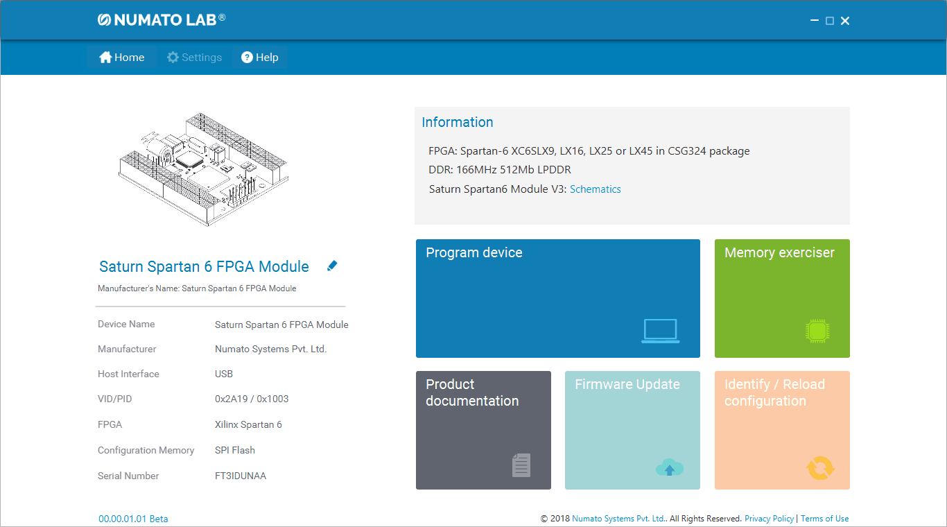
Tenagra Device Information Screen
Programming device using Tenagra:
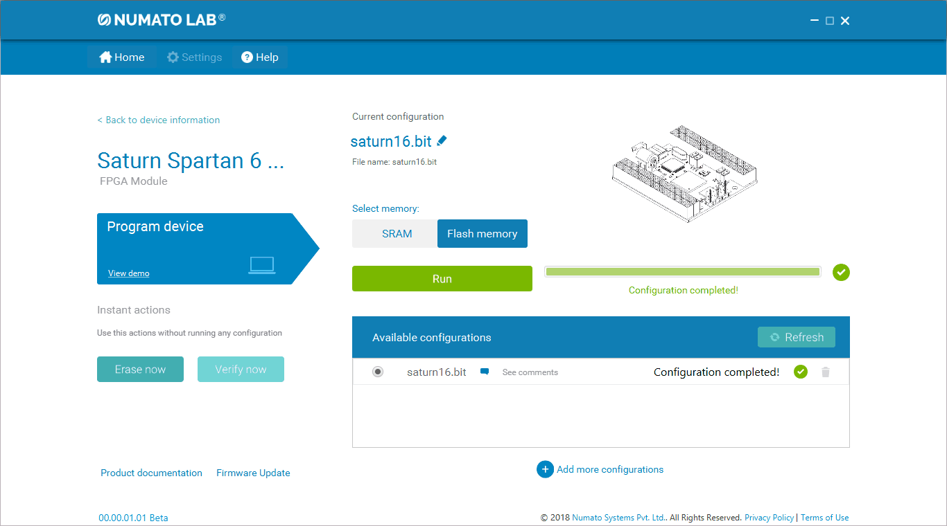
Programming Saturn Spartan 6 FPGA Module using Tenagra FPGA Management Software
Support
Finally, a critical factor in FPGA board selection is the support available to the users. Murphy’s law that says “Anything that can go wrong will go wrong” is a common epigram, even more so in the field of technology. Whether it is an issue with the FPGA board or an RTL design issue, problems with programming the board or installing the drivers or even setting up the board for the first time, helping our users in the best possible way is what we strive for. Compassionate support during these difficult times leaves a lasting impression on any customer. We believe all our customers are our brand ambassadors. Happy and satisfied customers are any company’s strength. At Numato Lab, we reply to most of the support queries within one business day, and our team meticulously works in resolving our customers’ issues to their satisfaction. If you have any queries or doubts or need to talk to us about anything, or even for a general chat, please email us at help@numato.com. We would be very happy to talk to you.
I would like to appreciate the vital contents in your blog.
April 11, 2019 at 8:36 amQuite an useful information. Thank you.
September 10, 2019 at 7:57 am