
Introduction

Tenagra is an FPGA System management tool for configuring and communicating with Numato Lab’s supported FPGA modules and development platforms. This software is designed to be a single interface for managing the devices and exercising some of the available features. Currently, Tenagra supports configuring the FPGA module/board (programming). With Tenagra, you can create multiple configuration setups with different bitstreams and settings for each device model so that switching between multiple bitstreams is a breeze. This is especially helpful during development where the device may need to be reprogrammed with various bitstreams repeatedly.
Boards Supported
A complete list of devices supported by Tenagra can be found below.
How to use Tenagra FPGA System Management Software
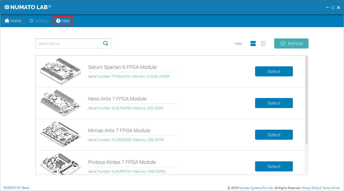
Home Page
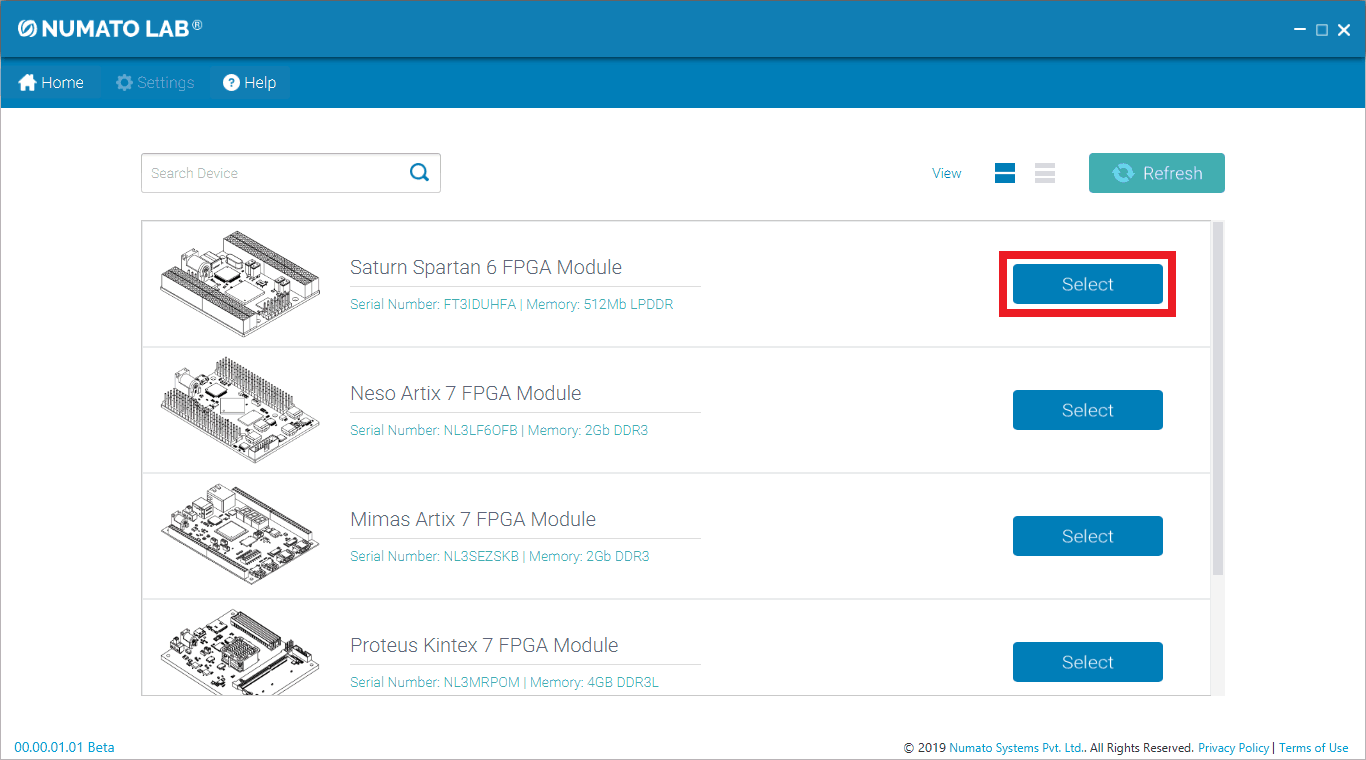
In the Home Page of the application, you will find the list of all the boards connected to the PC.
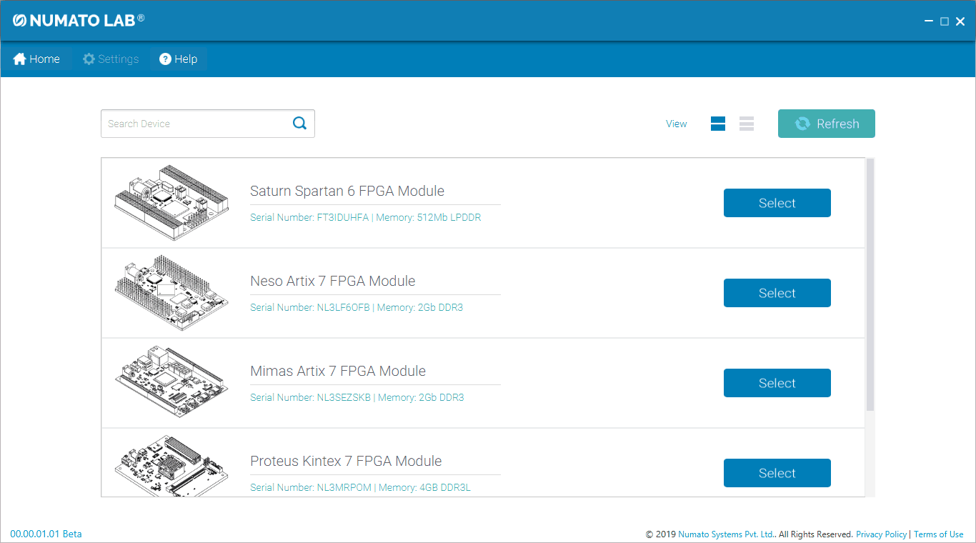
To know the device’s information and check the features, select the particular device by clicking on the Select tab present alongside the device name.
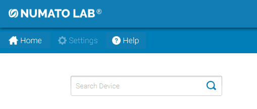
Search Device
When there are more devices connected, and you want to search a specific device, you can search for the device in the Search Device tab by entering information related to the board like the device’s name or it’s Serial Number or it’s Memory description.
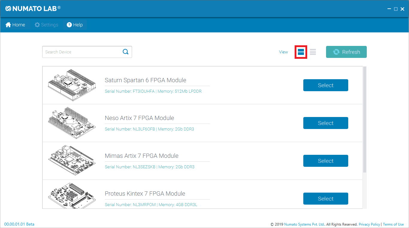
View
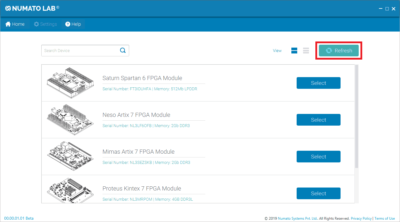
The view of the devices connected can be changed in the Home Page to ‘Grid’ or ‘List’ view by selecting the View options on the Home page.
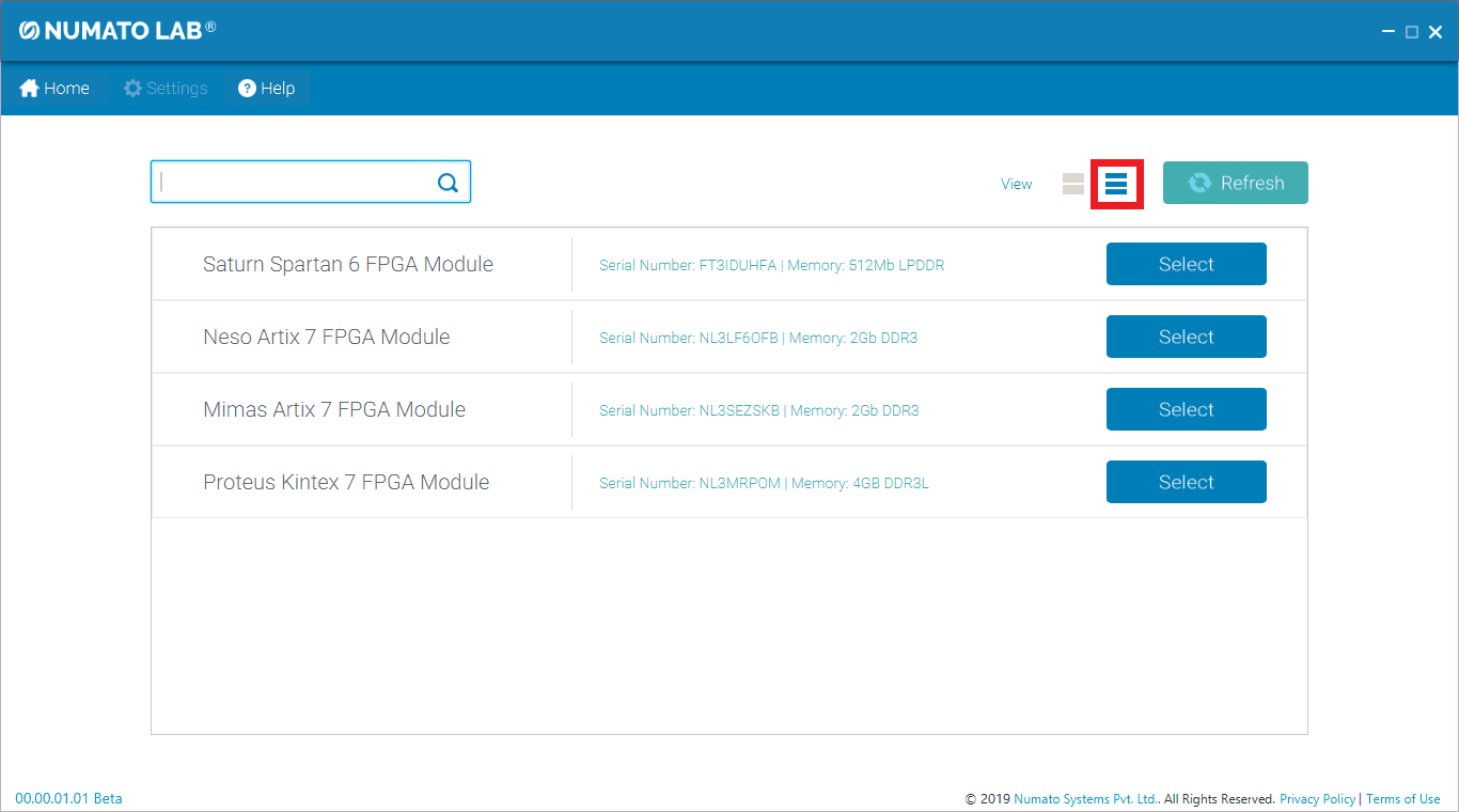
Grid View:
List View:
Refresh
After connecting a device to the PC, if it does not get detected, Refresh the page by clicking on the Refresh tab.
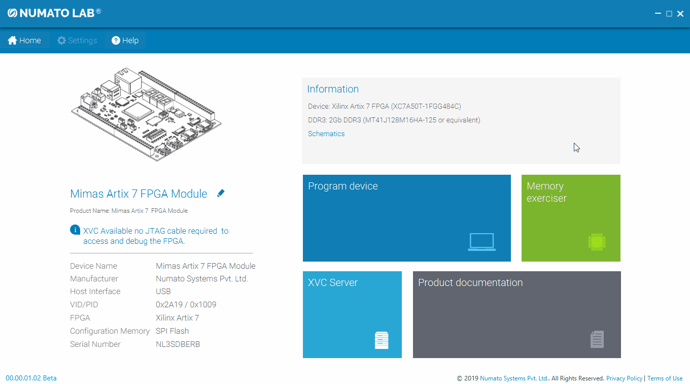
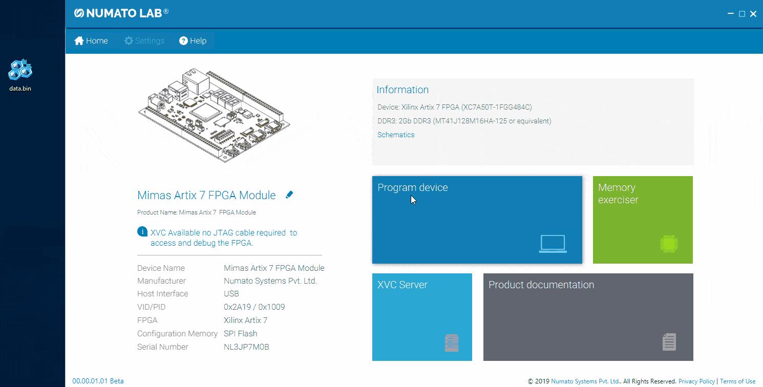
Device Information Page
Information

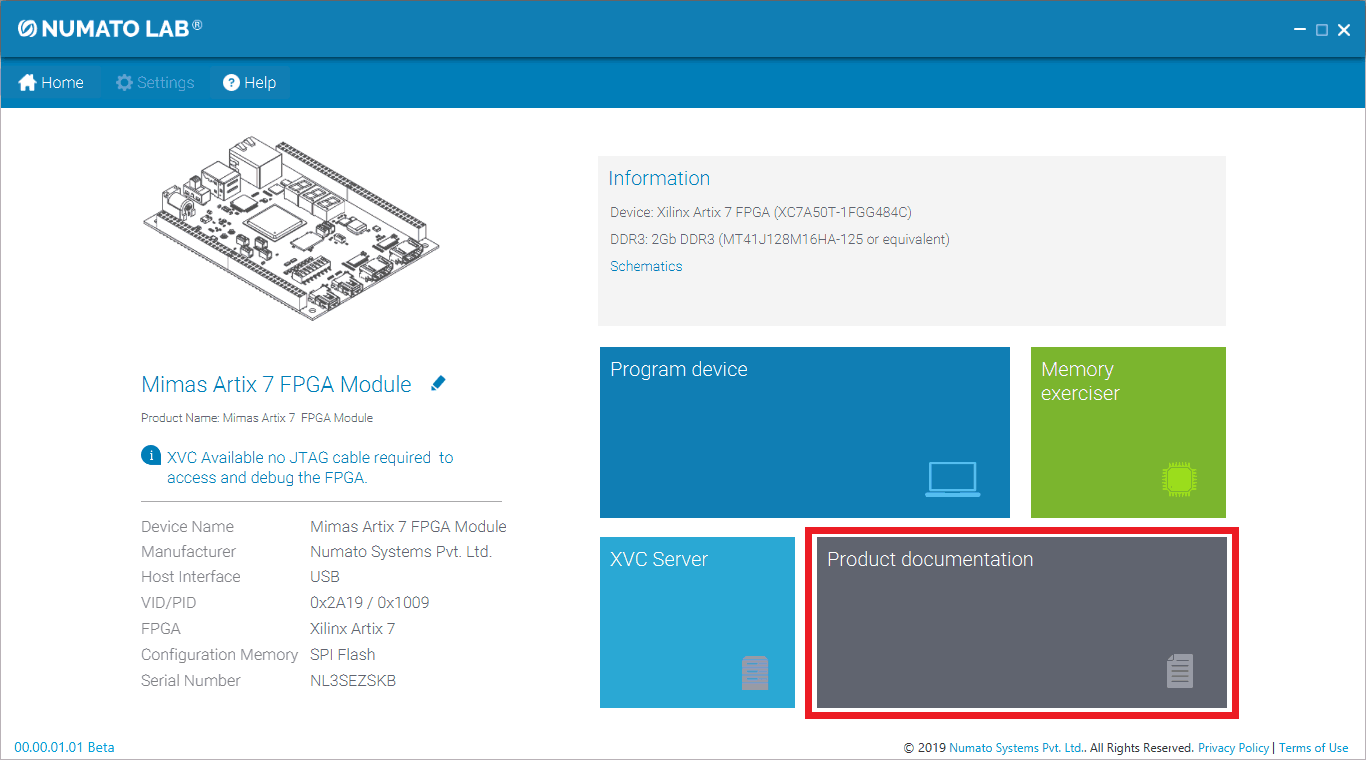
When a device is selected, the Device Information page will be displayed. On this page, all the details of the board will be present. The schematics of the board can be accessed from this page by clicking on the Schematics link present in the Information tab.
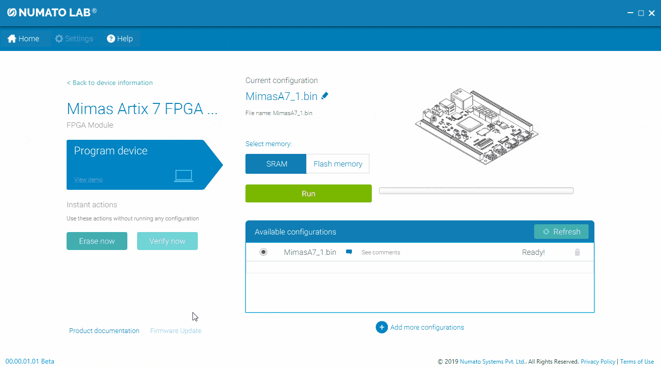
Program Device
Click on “Program Device” to program the board. Then to add Configuration Files click on “Add a configuration from your computer” button. Select the file which you wish to program on the board and then click on the “Run” button. This will program the board with the selected configuration file. The video below shows how to program a device in Tenagra.

Verify Now:
If you are testing the board and have programmed the board with different configuration files and now are confused as to which configuration file was last programmed to the FPGA, not to worry. You can now easily check the last file programmed in just a few steps. In the Program Device page, under Available configurations, select a configuration and then click on the “Verify Now” button (NOTE: before verifying, make sure that the board is booted from the SPI Flash else the verification will fail). This will verify if that particular file is present on the FPGA or not. The below video demonstrates the above-mentioned steps.

Erase Now:
When the board is programmed with a configuration, which you now wish to erase from the board, it can be done in just 2 steps. Just select the configuration file you wish to erase and click on the “Erase Now” button.
Product Documentation
When a board is selected, in its Device Information page, you can access the User Manual present on our website by clicking on the Product Documentation tab.
XVC Server
Xilinx Virtual Cable (XVC) is a TCP/IP based protocol that emulates JTAG protocol and acts like a JTAG cable over the network. Xilinx Virtual Cable provides a way to access the JTAG chain on the target FPGA board and debug the target without the need for a physical cable.
This can be done using the Tenagra application. In the Device Information page, click on the XVC Server tab to start the XVC Server. Then open Vivado–>Hardware Manager. In Hardware Manager select Open Target –> Open New Target. In the window that appears, click Next –> select Local Server –> Next –> click on Add Xilinx Virtual Cable (XVC) –> give the IP Address of your PC –> OK –> the device will be detected under Hardware Devices –> Next –> Finish. Now Program the device by selecting the configuration file. After programming, go to the Tenagra application and click on the XVC Server tab to stop XVC Server. These steps are illustrated in the video below.
Memory Exerciser
Memory Exerciser feature can be used to transfer data between Source and Destination. The options for Source are Random data, Data Pattern, File, DDR SDRAM, and Block RAM. For Destination: File, DDR SDRAM, and Block RAM. Data can be transferred between any of the Source and Destination.
The board has to be programmed with a bitstream for the Memory Exerciser feature to work. This bitstream can be found in the application’s installation directory where the application is installed. If the path where the application is installed in C:/Program Files (x86)/Numato Lab, the bitstream can be found in the path “C:\Program Files (x86)\Numato Lab\Tenagra\app\data\config\bitstreams”. Use the bitstream of the board you are using.
If the board is programmed with some other bitstream and if you use memory exerciser features and try to transfer, the application will automatically try to program the board with the respective bitstream. It might take up to 2-3 times to program the board.
Random Data:
You can transfer a random set of data to either a file or to DDR SDRAM or to Block RAM. The length of data to be transferred can be customized under Customize Data section –> Source Length (the length has to be a multiple of 4. Else the transfer will fail).
If you are transferring data to a file, select a file to which the data is to be transferred and then click on the Transfer button. When you open the file to which the data s being transferred you can find the Random data written to that file. The data will be in Hexadecimal form.
To transfer Random Data to DDR SDRAM, specify the Source Length (a multiple of 4) and the Destination Address has to be 0x0 and the Destination Length will be the same as the Source Length. Then click on the Transfer button. If you wish to check the data that is being written to the DDR SDRAM, under Sources select DDR SDRAM and under Destination select File. The Source Address will be the same ie., 0x0 and the Source Length can be the number of bytes you wish to read from DDR SDRAM.
To transfer Random Data to Block RAM, the steps will be the same as DDR SDRAM, but here the Source Address will be 0xC0000000. To read the data written to the Block RAM, follow the same steps as mentioned for DDR SDRAM above.
Data Pattern:
Here you can transfer a certain pattern ie., n number of bytes (user-defined pattern) to any of the Destination. The pattern length has to also be a multiple of 4. The bytes have to be separated by a comma. For example: 76, 90, 43, 15. If this pattern is transferred, data in the Destination will be in the format “76 90 43 15”.
The steps to transfer the data to the destinations are the same as the steps mentioned for Random Data transfer.
File:
Here, we can transfer any type of file to destination ie., file can be .png, .bin, .bit, .log etc. Any file format can be transferred.
For a file to file transfer, select the file you wish to transfer and a file to where it has to be transferred and then click on the Transfer button.
For the transfer to DDR SDRAM, select the file to be transferred and the destination address should be 0x0 and then click on the Transfer button.
To transfer to Block RAM, the destination address has to be 0xC0000000.
DDR SDRAM:
If you wish to transfer the data present in DDR SDRAM, select DDR SDRAM as the Source.
You can transfer the data present in DDR SDRAM to a file by selecting File as destination and the source address should be 0x0 and select a file to transfer the data, then click on the Transfer button.
Data can also be transferred to DDR SDRAM. When DDR SDRAM is selected as a destination, the destination address has to be 0x0.
To transfer data to Block RAM, select Block RAM as destination and the destination address should be 0xC0000000, then click on the Transfer button.
Block RAM:
If you wish to transfer the data present in Block RAM, select Block RAM as the Source.
You can transfer the data present in Block RAM to a file by selecting File as destination and the source address should be 0xC0000000 and select a file to transfer the data, then click on the Transfer button.
Data can also be transferred to DDR SDRAM. When DDR SDRAM is selected as a destination, the destination address has to be 0x0.
To transfer data to Block RAM, select Block RAM as destination and the destination address should be 0xC0000000, then click on the Transfer button.
The transfer log can be checked in the “Show log” section. The log can be cleared by selecting the “Clear log” button.
All the above-mentioned steps and transfers are demonstrated in the video below.
Help Page
When you click on the “Help” button, it will direct you to the Numato Lab Help Center page. If you require any help regarding the application or any help regarding Numato Lab’s products, you can find it on this page. You can also contact us for more information. Link to contact us is present in Numato Lab Help Center page.